Note: Descriptions are shown in the official language in which they were submitted.
Wt~ ~2/0~734 2 ~ Pcr/us91/06422
--1--
ACOUS~C C~RGE T~ANSPO~T IMAGE:E~
TECIINICAL~CKGROIJND.
T.ll;s invcntion relatcs to a sin~lc chip, low cost camera elcment
for Migh Definibon Tc]cvision (HDTV). ~forc spccifically the invcntion
rclates to the use of acoustic chargc transport ;n a ~allium arscnide (GaAs)
substrate to achievc high speed read out of photogcnerated c]cctric charge.
BACKGROUND ART
Existing HDTV cameras utilize a vacuum ~ube as the detecting
element. One example of such a tube is the I-I~RPICON H4318
15 manufactured by Hitachi. Although the HARPICON H4318 camera tube
provides ]ow no;se, h;gh sensit;vity perfonnance for HDTV app]ications, a
camera using th;s tubc is relatively large, fragile and heavy. Therefore, it is
not well su;ted for usc in light-weight app]ications such as hand-he]d HDTV
broadcast carneras, camcorders, or spacc app]ications. For thesc app]ications
20 a compact, light-wei~ht, comp]cte]y solid state dcvicc is idea].
The conventional choice for a solid-statc camera chip is onc
which uses a charge coupled device ~CCD) to read out the image chargc.
However, there is presently only onc CCD camera for I-IDl`V which can
25 operate at thc required video framc rate. This camcra, manufactured by
Toshiba, is very costly and there~ore unsuitab]e for consumer applications.
The HARPICON H4318 achieves high sensitivity and reso]ution
30 by ava]anche multip]ication induccd gain within the dctcction stagc, whicl1 is
made from amorphous selenium (a-Se). Howevcr) the use of an a-Sc
detector stage means that holc transport and collcction arc rcquircd bccausc
WO ~2/04734 PCr/US9~/06422
the hole ionization rate is substantially highcr than thc elcctron ionization
rate in a-Se. I-Iolc transport is not compatiblc witll high spcecl inte~rated
circuit operation.
Thercfore, thcrc is a nccd for a small, low-cost, lo~v voltage,
ea~sy to manufacture, rcliablc, high rcso]ution HDTV camera elcment,
capablc of read out specds compatiblc with HDTV framc rate requirements.
DISCI,OSIJRE OF T~IE TNVENTION
Accordingly, thc general object of the invention is to provide a
mecms for detecting light in the visib]e spectrum with an imager array
sufficiently large to achicvc ~ TV resolution and to couple the imager array
to a means for read out which operatcs at sufficiently high speeds so as to
15 achieve compatibi]ity with HDTV framc ratcs. The devicc of the present
invention wou]d a]so bc suited for many spccial typcs of fast imaging
app]ications, such as high reso]ution super-slow-motion or fast processing
app]ications, such as on-chip ima~c enhancement.
It is an object of the present invcntion to coup]c a ]ow-noisc,
high-gain photodctector element to a means.capab]c of high speed charge
read out.
It is anothcr object of the present invention to monolithically
combine heterostructure acoustic charge transport (ACI) devices and
amorphous hydrogenated silicon avalanche photodiodes (APD).
It is a further object of thc present invention to achievc an
ima~er architecturc which is both acoustically and optically efficien~.
O 92/1~1734 2 ~ 5 PCI/US~1/06422
It is a furthcr object of the prcsent invention to provide a so,'ld-
state camcra chip ~or HDTY applications.
It is a ~urthcr objcct o~ this invcntion to providc such a chip
.~ wllicll is small ancl cfricicnt enou~h to bc uscd in camcordcrs and spacc
applic<ltions.
It is yet a further object of this invention to provide such a chip
made from an ~CT structure in a GaAs substrate and ~m APD constructed
10 from amorphous silicon to providc an cfficient .md integrated system for use
with HDTV equipment.
It is still a further object of this invention to provide such a chip
which globa]ly optimizcs pcrÇormance of the heterostructure by balancing the
15 photodetector and ACI' rcad out structllre design parameters.
The invention comprises four main components: (1) a
photodetector which may be an amorphous si]icon avalanchc photodiode
(APD), or a super]attice APD, (2) an npn bipolar junction transistor (BJT)
2d to provide char~,e stora~,c and clamping action, (3) an acoustic charge
transport (ACT) structure in which char~e is rcad out for imagc
reconstruction, and (4) a metal-insulator-semicorlductor field effect transistor(MISFET) structure to controllably transfer, that is gate, the stored charge
into the ACr channel. These four componcnts arc integrated in a compact,
25 comp]etely solid-state device suitablc for use in light-weight applications such
as hand-hcld HDTV broadcast cameras, camcorders or space appl;cations.
This structural combination of the prcsent invention is novel.
Several materials choiccs arc available for both thc
30 photodetector and ACI structures. The photodetector may be silicon bascd
or fabricatcd from a compound semiconductor matcrial system. Althou h a
W~ 92/04734 ~ PC~r/US91/06422
C~aAs photodetector has ccrtain theoretical advantages, such as improved
gain, ovcr a silicon photodctector, thc GaAs photodctector has a number of
problcms re~ated to rnanufactulabi1;ty. Thc substratc in which the ACT
structurc rcsidc~ may bc G~u~s/~]GaAs or somc othcr snatcrial systcm such
5 as silicon Wit]1 ~n associated piczoclectric laycr. ~ny substratc materia]
system, or combination, that supports acoustic charge transport can be used.
In the preferred embodiment, the ~PD is made from an
amorphous silicon. This type of APD uses electrons as thc initiating carriers,
10 allowing it to yield low noise pcrformance while still being compatible with
the ACI~ component. The particular ad~antage of amorphous si]icon is its
reproducibility, cost effectiveness, uniformity, and potential ]ow noise
perforrnance.
~5 The charge from thc APD is co]]ected in thc emitter region of a
bipolar junction transistor (BJT) and is then gated into an ACT channe].
The ACI componcnt to which the APD is coup]ed in the prcferred
embodiment uti]i~es a GaAs/AlGa~s structurc which is capab]c of very high
speed, high efficiency charge transfcr, thus enab]ing higher frame rates than
20 have previously been possib]e with charge coup~ed devices (CCDs). Thc
speed of the ACT can be attributed to high electron mobi]ity and a potential
which is propagated with a surface acoustic wave ~SAW3 instead of a
potential imposed by clock pu]ses, as can be found in previously existing
CCDs.
BI~rEF I~SCRIPIION OF T~IE DRAWINGS
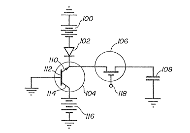
Fig. 1 is a circuit schematic representing one imagcr ce]l
showing the interconnections betwcen thc APD, the BJT, thc ~ISFET
30 transfer gate and the ACT channe].
WO ~2/04734 PCT/US91/06422
Fig. 2 is a cross sectional view of one imager cell illustrating thc
spatial relabonship of the clements comprising the ce]l.
F;g. 3 is a block dia~r~m showing a two dimcnsiona~ imager
5 array and a hori~ontal ACI ch~r~c rcad out rc,gistcr.
l~EST MODE OF CA~YING OU'I' TI-IE INVENTION
The preferred embodiment of the invention is now described
10 with referencc to tlle drawings.
1. Electn'cal,_CQnncctivi,t,v
Referring now to Fig. 1, there is shown a schematic
15 representation of one cell of the acoustic charge transport imager in
accordance with the present invention. The cell includes an avalanche
photodiode (APD) ~02, an npn bipolar junction transistor (BJT) 104, a
MISI;ET 106, and an acoustic charge transport channcl represcntcd here as a
capacitor 10~S. The APD 102 has its p region connected to a volt~gc sourcc
20 100 which is negative with respec~ to ground. The emitter 110 of BJT 104
forms a common node with the n region of APD 102. The base 112, of BJT
104 is connected to ground. The collector 114 of BJT 104 is connected to
the positive voltage supp]y 116 of the substrate. The common node of BJT
104 and AI'D 1û2 is couplecl to the ACT channel 108 through the MISFET
25 1(~6. A control signal is connected to the MISFET gate 11~ terrnina].
2. Phv~ical Structure
The four main elements of the imager ce]l, the APD, the BJT,
30 the MISFET and the J4C~ channel, are compatible with each other and
suitable for monolithic integration. Fig. 2 shows a cross section of thc
WO 92/04734 ~ pcr/uss]/oG422
physical architecture of thc cell. In this view, the ACI channcl runs
perpendicul~rly through the plane of the figurc.
Thc ~PD of thc prcfcrrcd embodimcnt is cornprised of a p typc
S rc~ion 21)'1, an intrinsic region 206, and an n type rcgion 20S. The p typc
region 204 is rnadc ~om ~unorphous hydrogenated silicon carbide (a-Si,
,~C~:(H) whcre O<x<1). Thc intrinsic re~ion is made from an amorphous
hydrogenated silicon (a-Si:(:EI)). The n type region is made from polysilicon.
In the art to vhich this învention pertains, polycrystalline silicon is referred
10 to as polysilicon.
~ n electrode 202 which is transparcnt to some portion of thc
electromagnetic spectrum forms the top surface of thc APD. In the
preferred embodiment of the prescnt invcntion this electrode ~02 is
1~ tr~nsparent to the visible portion of the spectrum and is comprised of an
indium-tin-o.cide (ITO) layer. This ITO layer of the preferrcd embodiment
does not require a passivating topside layer. The ability to fabricate this
structure without a topside layer simplifies opb'cal and acoustic design
considerations.
Whcn photons pass through the transparent e]ectrodc 202 and
ineo the reverse biased APD, a current is generated. This currerlt passes out
of the diode through an n-doped po]ysilicon plate 208 and an n-doped
polysilicon pillar 214 into the n~ emitter 226 cf a vertical npn BJT. The flat,
25 rectangu~ar polysilicon plate 208 may be fabricated in alternatiYe shapes, such
as circular and/or non-planar. The preferrcd embodimcnt utilizes a
polysilicon region having two major surfaccs.
~ channel stop 218, comprising a p~ region, abuts thc I3JI` and
30 MISFET structures. In the preferred embodiment thesc p+ rcgions are
forrned by Be doping. Ion implantation of Be is thc prcferrcd mcthod of
wo 92/1)4731 Q ~ T CI`/US9l/OG422
achieving said doping. rhe channel stops serve to electncally isolatc thc BJT
and MISFET structures from other electrical elements and signals which mc-ly
be present in or on the ima~cr chip.
The channel stops 218 of thc prcf~rrcd cmbodimcnt arc
dcsi~ncd as long stlips which run through thc imagcr array, with thc ground
contacts formed nt both ends. Thc shect resistancc and ]cngth of the
implantecl channel stop strips must bc considered carcfully during the design
stages in order to avoid fonvard biasing. Any currcnts passing through the
channel stop str;ps wi]l act to dcvclop somc voltagc (V=IR). If thc voltagc
in some part of the channcl stop strip becomes greater than the diode turn-
on voltage then unwanted conduction will takc placc. One result of this
unwanted conduction is corruption of thc stored ima~e data.
A ]ight shield 210 having two major surfaccs, scrves to isolate
the underlying BJT, MISF~T and ACT channel from pcrformanc~ degrading
photons. In the preferred embodimcnt the ]ight shicld is formcd from a
layer of molybdcnum.
If the light shie]d is formcd from a conductivc material, such as
molybdenum, then it must be electrically isolated from thc photodctector. In
the preferred embodimcnt an insu]ating material is disposcd between the
photodetector (including the conductivc pil]ar~ and thc light shie]d.
Additiona]ly, a conductive light shie]d should be grounded in ordcr to
eliminate the possibility of trapped charge in the light shic]d. Charge
trapped in the li~ht shield may advcrsely afrcct
the performance of the underlying MISFET structurc. Such effects might be
manifested in shifts of MISFET thicl~ fic]d thresho~d voltage.
The li,ht shie]d 210 is physically and clectricallY separated from
the underlying BJT, MISFET and ACT ch~mncl by a die]ectric laycr 212. In
w~ 92/04734 ~ PCI/US91/06422
the preferred embodiment phospho-silicate-glass (PSG) is uscd as the
dielectric layer although other dic]ectric materia~s, such as boro-phospho-
silicate glass (BPSG), ZnO or BaTiO, may a]so be suitablc.
Both ZnO and BaTiO, can bc used to crcatc an insulating ]aycr
which is also a piezoelectric film. If a material is chosen ~vhich is more
piezoelcetric than the Ga~s substrate, a surfacc acoustic wave can be
generated havin~ a deeper potentia] well than could be obtained in GaAs
alone. That is, the voltage potentia] developed by the SAW would be larger.
The MISFET structure consists of a gate e]ectrode 222, a
die}ectric 224, and scmiconducting material 230. In the present invention thc
gate electrode is separated from the semiconductor material by thc dielectric.
Said dielectric may be either Si3N,, or undoped G~s. As can be seen in Fig.
2, the gatc 2?2 physically spans a region in which an ~iCI channel e.~ists, as
well as a }atera}ly adjoining p re~ion and a portion of the n+ emitter 226
region.
The BJT portion of the present invention is fabricatcd using the
n substrate 220 as the collector. A p type basc 228 region is then fonned
vertica]]y above the col]ector. The corresponding n~ emitter 226 is fonned
above the base, as shown in Fig. 2, so that taken together there is an npn
stack.
The ACI' device operation requires confinement of the charge
to be transported, within a thin ]ayer 234 of GaAs sandwichcd bctween two
relatively tnicker laycrs of AlGaAs 230, 236. The GaAs quantum well 234 is
undoped while the ]ower AlGaAs layer 230 is p type dopcd and the top ]ayer
236 is lightly n dopcd. In the preferrcd cmbodimcnt, Bc is thc dop~nt used
to achieve p type doping in the lower AlGaAs ]ayer.
WO 92/Q47~4 ~ ; Pc~r/us91/06422
3. Ima~er Operation
Light from an object to bc ;magcd is focused upon an array of
photodetcctor clcmcnts. Thc prcfcrrcd cmbodimcnt utili~es a two-
5 dimcnsionn1 array. The numbcr of photons incidcnt at any particular pointon the array is a function of the object being imaged. Thc photodctcctors
generatc an electrical charge proportional to thc number of incident photons.
This plloto~eneratcd chargc, which e]ectrically rcpresents an image of the
object, is temporarily stored. A]ternatively, this process could be described as10 converting electroma~netic imagc inforrnation into a two dimensional array
of discrete analog charge packets and thcn storing those packets.
In order to transfcr thc stored image information from a largc
numbcr of photodetector elcments it is necessary to usc a seria] read out
15 technique. Howcvcr, in order to mect HDTV vidco framc rate
requirements, the serial read out must be fast.
Higll speed read out, or accessin~, in the prescnt invention~ is
achieved by gating the stored charge into channe]s where an e]ectric
20 potential, resulting from a surface acoustic wave, swecps the charge to othcr chip circuitry for further processin~.
The imager cells 302 are arranged in a two dimensiona] array
304 of rows and co]umns as shown in Fig. 3. During the read out operation,
25 a paraliel trans~er of all the charge packets in a row of thc imager array toan intermediate storage row 30G is perforrncd by acoustic charge transport.
Each charge packet in the intermediate storage row ~6 is then scria~]y
transferred out, by means of acoustic charge transport, for further processing.
The novel cornbination of a silicon bc~sed photodetector with an
ACI read out structurc in GaAs can be used to form thc basis of a~tcrnativc
WO 92Jo4734 2 ~ pcr/us9l/oG422
read out schemes such as frame transfer. In a framc transfcr all the charge
packcts in the irnager array arc transferred en massc, rathcr than row by row,
to an cqually si~cd storagc array. This stora~c array is typical]y a non-
imagin,~ array.
~ dctailed description of the opcration of the im~gercomponcnts is included below.
By reverse biasing the APD, a depletion region is created within
10 the photodiodc whcrein current multiplication through impact ionization rnay
take place. Photons incident upon the imager generate the charge which
initiates current multiplication. This mult]plicd photo-initiated charge passes
to the emitter 110 of BJT 10~ and is stored therein.
Thc ~PD must be reverse-biased in ordcr to operate. Becausc
of this requirement, a transparent electrodc 202 is used to make e]ectrical
contact to the p sidc of thc APD.
C~arge rom the ~PD is stored primari]y by the capacitancc of
20 the emitter-basc junction. Although the emitter nodc of a BJT is uscd for
charge storage in thc prefcrred embodiment, other means for storing chargc,
such as a diodc or parallcl plate capacitor, may be uscd. A means for charge
storage is physical]y and clcctrically associatcd ~vith the photodetector
e]ements.
There are three possible mechanisrns by which this storcd
charge may movc. One mechanism is by way oi reverse-biased diode leakage
currents into the b~se and channe] stop regions. A second mechanism is thc
forward-biased diodc current which f]ows whcn tlle cmitter nodc bccomcs
30 negativcly biased with respcct to thc basc node bv morc than a diodc drop.
Wo 92/0~1734 ~ PCr/US9~/0()422
A third mechanism is the creation of a conductive pathway from thc charge
storagc nodc to thc ACT channcl by way of MISFET action.
Rcvcrsc-biascd cliode leakagc currcnt acts ovcr timc to corrupt
5 thc storcd ima~c data. This puts ~a practical limit on thc sizc of thc imager
array sincc thc ima~c data is read out esscntially serially. Scrial rcad out
mcans that a fin;te timc is required to access all the storage nodes in the
irnager ~ay. As the array becomcs larger the acccss cycle timc becomes
longer. The longer a storage nodc must wait to be accessed, the greater will
10 be the image data corruption due to rcverse biased diode leakage currcnt.
When a large number of electrons collect in the emitter of BJT
104, said emitter will become sufficiently negativc with respect to the
grounded base, so that the base-emitter diode will become forward biased.
15 Fo~ward biasing will result in current flow until thc numbcr of electrons ;s
sufficiently reduced so that the diodc turns off. The result of this action is
essentially to limit the amount of chargc availablc for rcad out. That is, the
magnitude o the stored charge is c]amped. This limits the imagcr dynarnic
range but minimizes blooming, which has becn a problcm for imagcrs of
20 older technology.
The usc of the vcrtical BJT structurc to remove excessive
charge is a particular]y useful feature of the preferred embodiment. Without
the use of the BJT, excess charge wou]d pass into the channel stop. Current
25 in the channel stop creates a voltage, the magnitude of which is a function of
the current and the channel stop sheet resistivity. The vo]tage dcvc]opcd
could possib]y forwarci bias some channel stop-emitter junction resulting in
ima,6e data corruption. The BJT of the present invention conducts the excess
char~e into the substratc.
wO 92/04734 ~ ~3 ~ ~ 3 ~ 5 PCr/US91/06422
Chargc transfer from storage node to ACT channel occurs whcn
a conductivc pathway between them is created by action of thc h~lSFET
structure. Thc MISIET structurc providcs a mcans of controllab]y
transfcrring chargc from thc storagc nodcs to thc Acr channcls.
Oncc thc chargc rcprescnting thc image data has bccn
transfcrrecl to thc ACr channc] ;t is swcpt along by thc potcntial resu]ting
frorn a sur~ace acoustic wave. The SAW forces the charge a]ong the channe]
to that part of the chip where further processing may take p]ace.
It is to be understood that the forms of the invention described
and illustrated herein are to be taken as preferred e.l~amples of the same and
that various changes in the arrangcmcnt of components or type of matcria]s
may be made without departin~ from the spirit of the invention or scope of
15 the claims.