Note: Descriptions are shown in the official language in which they were submitted.
- ~ 2091 1 1 1
SOCKET AND HEADER ELECTRICAL CONNECTOR ASSEMBLY
FIELD OF THE INVENTION:
The present invention relates to a connector asse~mbly
including an interconnectable socket connector and header
connector. More particularly, the present invention relates to
a connector assembly for easily releasably connecting an
electronic apparatus housed in a socket connector to a header
connector.
BACKGROUND OF THE I~v~NllON:
In establishing electrical connection between various
components, especially in the electronics environment, socketing
has long been used as an expedient. Socketing entails providing
a pair of connectors which are matable. One connector of the pair
typically houses an electronic apparatus while the other
connector of the pair is mounted and electrically secured to an
object to which connection is desired such as a printed circuit
board. Where connection is desired between an electronic
apparatus and a printed circuit board, the first connector is
usually referred to as a socket connector while the second
connector is usually referred to as a header connector.
In addition to providing ease of interconnectability, the
socket connector is also used to provide physical protection to
the electronic apparatus housed therein. Socket connectors may
be constructed which totally enclose an electronic apparatus
housed therein to prevent external cont~mln~nts from adversely
affecting the electrical performance of the apparatus. However,
in certain extremely harsh environments, such as those found in
the engine compartment of an automobile, merely covering the
electronic apparatus may be insufficient protection.
The art has seen the use of encapsulation techniques where
the electronic apparatus is encapsulated or potted, with a
curable potting compound. The potting compound is typically
provided in a fluid state, which after being poured around the
electronic apparatus, hardens or cures to a solid state, thereby
providing an environmental seal around the electronic apparatus.
Socket connectors, which support such electronic apparatus, must
be also capable of containing a curable potting compound in such
'
209 1 1 1 1
a manner that complete encapsulation of the electronic apparatus
is achieved.
In order to facilitate mass production of such socketed
connectors, the socket connector should support the electronic
apparatus in such a manner that it is relatively easy to
completely encapsulate with potting material.
SUMMARY OF THE INVENTION:
It is an object of the present invention to provide a
socketable connector assembly which permits the releasable
matable interconnection of electronic components.
It is a further object of the present invention to provide
a connector assembly for electrically connecting an electronic
apparatus supported in a socket connector to a header connector
supported on a printed circuit board, and where the socket
connector is easily releasable from the header connector.
In the efficient attainment of these and other objects, the
present invention provides a connector assembly for electrically
connecting an electronic apparatus to a printed circuit board.
The assembly includes a socket connector and a matable header
connector. The socket connector includes an insulative open-
sided container which is capable of retaining a curable potting
compound. A plurality of electrical contacts are supported by
the container having first ends within the container which engage
and support the electronic apparatus. Opposed second ends of the
contacts extend exteriorly of the connector. Means is provided
for supporting the electronic apparatus in a position within the
container to permit the electronic apparatus and the first ends
of the contacts to be surrounded by the potting compound. A
cover is supportable over the container to enclose the potted
electronic apparatus. The header connector is securable to the
printed circuit board and includes an insulative housing and
plural electrical terminals electrically engageable with the
socket contacts to establish electrical connection therebetween.
As more particularly shown by way of the preferred
embodiment, the invention provides for the interconnection of a
pair of components. A first component housing and a second
component housing are interconnectable. Cooperative latching
. !
~,091 ~ ~ ~
means secures the first component housing to the second component
housing. The latching means further includes a latch member
connected to the first housing by a pivotal hinge. The latch
member includes a pair of elongate arms depending from the hinge.
Ends of the arms include engagement ledges thereon. A pair of
manually graspable tabs extend from the hinge and are moveable
about the hinge toward and away from one another to cause
corresponding relative movement of the ends of the latch arms.
The tabs are also moveable in unison about the hinge toward and
away from the first housing to cause corresponding movement in
unison of the ends of the latch arms. The second housing
includes a ledge engaging protrusion formed thereon for
engagement with the ledges of the latch member. The ledges of
the latch member are disengagable with the protrusion upon
",o~enRnt of the tabs about the hinge either toward or away from
one another or in unison toward and away from the first housing.
BRIEF DESCRIPTION OF THE DRAWINGS:
Figure 1 shows in exploded perspective view, the socket
connector of the connector assembly of the present invention.
Figure 2 is a perspective showing of a header connector of
the connector assembly of the present invention.
Figure 3 shows an electrical contact used in the socket
connector shown in Figure 1, attached to an electronic apparatus.
Figure 4 shows the socket contact and the electrical
apparatus shown in Figure 2, supported by a housing of the socket
connector of Figure 1.
Figure 5 shows partially in section, the assembled socket
connector of Figure 1.
Figure 6 shows partially in section, the assembled socket
connector of Figure 5 inverted and connected to the header
connector shown in Figure 2.
Figure 7 shows a further embodiment of the socket connector
of the present invention.
Figure 8 shows a further embodiment of the header connector
of the present invention.
Figure 9 shows the socket connector of Figure 7 connected
to the header connector of Figure 8.
~f
2091 1 1 1
DETAILED DESCRIPTION OF THE PREFERRED EMBODIMENTS:
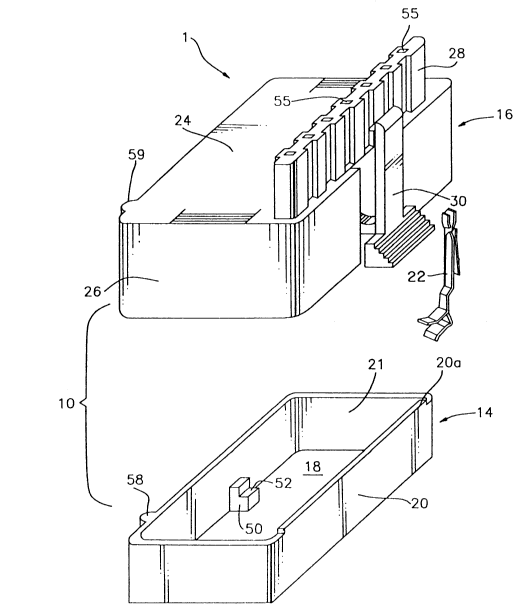
The electrical connector assembly 1 of the present invention
is shown in Figures 1 and 2. Connector assem.bly 1 includes a
socket connector 10 shown in Figure 1 and an intermatable header
connector 12 shown in Figure 2. Socket connector 10 is formed of
a suitable electrically insulative plastic material and as shown
in Figure 1 includes a lower housing 14 and an upper cover 16.
Lower housing 14 is generally rectangular in shape having a
planar bottom wall 18 and an upstanding side wall 20 extending
about the perimeter of bottom wall 18. The upper surface of
lower housing 14 is open thereby forming an open-ended container
which is closed by cover 16. Lower housing 14 and side wall 20
define an internal cavity 21.
Socket connector 10 further includes plural electrical
contacts 22, one of which is shown in Figure 1. Contacts 22 are
positioned on lower housing 14 in a manner which will be
described in further detail hereinbelow.
Cover 16 is also generally rectangular in shape, having a
planar upper wall 24 and a depending side wall 26 extending
perimetrically around upper wall 24. Cover 16 is constructed to
fit over lower housing 14 to enclose cavity 21 thereof. Cover
16 includes an upwardly extending portion 28, which permits
accommodation of contacts 22 as will be described in further
detail hereinbelow. Cover 16 also includes a latch 30 mounted
on side wall 20. Latch 30 is m~n~ ly operable to secure and
lock socket connector 10 to header connector 12, as will be
described in further detail hereinbelow.
Referring additionally to Figure 3, socket connector 10 is
designed to house an electronic apparatus 32 which may include
a printed circuit board 34 upon which are mounted various
electronic devices 36. Electrical contacts 22 are used to
establish electrical connection with electronic apparatus 32.
Contacts 22 are elongate members formed of suitably electrically
conductive material, and include a first end conventionally
formed into a pin receiving socket 38. Each contact 22 further
includes an elongate central portion 40 extending from socket 38
to a connecting clip element 42 at the opposite end thereof.
Clip element 42 is used to engage an edge 34a of printed circuit
2091 1 1 1
`_ S
board 34. Clip element 42 includes upper and lower fingers 44
which engage opposed surfaces of printed circuit board 34 about
edge 34a. Fingers 44 typically electrically engage metallic
traces (not shown) on the surfaces of printed circuit board 34
to establish electrical connection therebetween. Central portion
40 of contact 22 includes an angled transition region 46 which
horizontally spaces clip element 42 from socket 38.
In the present embodiment, it is contemplated that socket
connector 10 will employ eight contacts 22. The contacts 22 are
spaced along edge 34a of printed circuit board 34. The clip
elements 42 of contacts 22 secure contacts 22, both mechanically
and electrically to printed circuit board 34. It of course may
be appreciated that a socket connector may be constructed which
could support a various number of contacts 22 as may be needed
for a particular application.
Referring now to Figure 4, the electronic apparatus 32 and
contacts 22 which are secured thereto, are inserted into lower
housing 14. Socket contact 22 includes a wall engaging portion
48, shown in Figure 3, which clips onto an upper edge of 20a of
side wall 20. The engagement of each of contacts 22 with the
upper edge 20a of side wall 20 secures the contacts thereto and
also fixably supports electronic apparatus 32 within cavity 21
of lower housing 14.
Contacts 22 are constructed so that central portion 40
thereof extends down toward bottom wall 18, but terminates in
clip element 42 at a location spaced from bottom wall 18. Thus,
as shown in Figure 4, clearance is provided between printed
circuit board 34 and bottom wall 18. Additionally, as shown in
Figures 1 and 4, lower housing 14 includes a platform 50
extending upwardly from bottom wall 18 at a location spaced from
contacts 22. Platform 50 includes a board bearing surface 52,
which is substantially parallel to bottom wall 18 and which
supports an edge 34b of printed circuit board 34 opposite to edge
34a. Platform 50 helps support printed circuit board 34 within
cavity 21 at a location spaced from bottom wall 18. In addition,
as particularly shown in Figure 4, transition region 46 of
contact 22 disposes clip element 42 at a location spaced inwardly
from side wall 20. This provides a clearance between clip
g
209 1 1 ~ ~
element 42 and side wall 20. Further, board bearing surface 52
of platform 50 is spaced inwardly from side wall 20. Thus, as
positioned in Figure 4, printed circuit board 34 is positioned
centrally within cavity 21 spaced from side walls 20. By spacing
printed circuit board 34 away from both bottom wall 18 and side
wall 20 of lower housing 14, clearance is provided on all sides
of printed circuit board 34 which permits complete encapsulation
of electric apparatus 32.
Referring now to Figure 5, as electronic apparatus 32,
including printed circuit board 34, is spaced both vertically and
horizontally away from bottom wall 18 and side wall 20 of lower
housing 14, a potting compound 56 may be poured into cavity 21
of lower housing 14 to completely surround electronic apparatus
32 as well as clip elements 42 of contacts 22 which engage
printed circuit board 34. Potting compound 56 is of the type
which is commonly used and commercially available in the
electronics industry to environmentally seal electronic
components. It is typically provided in a fluid state so that
it may be poured into cavity 21 of lower housing 14, to flow
completely around electronic apparatus 32 and clip elements 42
of contacts 22. The potting compound 56 is permitted to cure to
a hardened state whereby the electronic apparatus as well as its
electrical connection to contacts 22, are environmentally sealed.
Once potting compound 56 hardens or cures, cover 16 may be
placed over lower housing 14 to enclose the potted electronic
apparatus 32. As shown in Figure 1, lower housing 14 and cover
16 may include cooperative key element such as a rib 58 on lower
housing 14 and a slot 59 on cover 16 to provide keyed-matability
between cover 16 and lower housing 14.
Extending portion 28 of cover 16 accommodates extending
sockets 38 of contacts 22, securely retaining contacts 22 within
socket connector 10. Extending portion 28 includes openings 55
adjacent sockets 38 to permit electrical connection to sockets
38.
Referring now to Figures 2 and 6, the connection of socket
connector 10 to header connector 12 is shown. Header connector
12 includes an elongate insulative body 60, having a central
cavity 62 of like shape to that of extending portion 28 of cover
2091 1 1 1
_ 7
16 which is received therein. The shape of extending portion 28
and cavity 62 provides a keying feature preventing improper
connection of socket connection 10 to header contacts 12. Header
connector 12 includes a plurality of pin-type contact terminals
64 in num.ber corresponding to the number of contacts 22 in socket
connector 10. ~e~er connector 12 includes a latch receiving
member 66, which comprises a tapered lead-in portion 67 and a
securement portion 68. Latch receiving member 66 is engageable
with latch 30 to lock socket connector 10 to header connector 12.
It can be seen that latch 30 is employed by m~nll~lly
pivoting the upper portion of the latch about the hinge which
connects it to cover 16. Use in this manner requires that there
be sufficient clearance about latch 30 to enable a user to obtain
m~ml~l access to latch 30 and manipulate it back and forth to
lock and release socket connector 10 to header connector 12. It
is contemplated that the socket connector 10 and header connector
12 may be employed in areas which have limited access making it
difficult to access latch 30 along the side thereof to pivot the
latch. This limited access may be found in instances where the
he~er connector 12 is mounted on a printed circuit board 65
(Fig. 6) next to a wall of a housing (not shown) in which the
printed circuit board 65 is installed. In such cases there may
not be sufficient clearance to provide for the actuation of latch
30.
The present invention further contemplates use of an
improved latch design which would facilitate simple releasable
connection of socket connector 10 to header connector 12 even in
areas of limited access.
Referring now to Figures 7-9, cover 16 is shown having an
improved latch 70. Latch 70 is connected to cover 16 by an
intermediate hinge 72 in a manner similar to that shown in
Figures 1 and 6 hereinabove. Latch 70 includes a pair of
depending latch arms 74 and 76 which depend from hinge 72. Latch
arms 74 and 76 are separated by an elongate slot 78 therebetween.
The distal extents of latch arms 74 and 76 include engagement
ledges 80 and 82 respectively (shown in phantom in Figures 7 and
9) which are similar in structure to that shown in Figures 5 and
6. Latch 70 also includes a pair of m~nll~lly graspable tabs 84
2091 1 1 1
_. 8
and 86 which extend upwardly from hinge 72 as shown in Figure 7.
Tabs 84 and 86 are separated by a V-shaped recess 88
therebetween. The V-shaped recess 88 permits tabs 84 and 86 to
be moved toward and away from each other thereby causing opposite
corresponding movement of latch arms 74 and 76 toward and away
from each other about slot 78. This is in addition to the
conventional movement of latch 70 about hinge 72 where tabs 84
and 86 are moved in unison toward and away from cover 16 to cause
opposite corresponding movement of latch arms 74 and 76 in unison
about hinge 72.
Header connector 12 shown in Figure 8 is substantially
similar to that shown in Figure 2. The latch receiving member 66
is slightly modified to have a smaller longitl]~;n~l extent so as
to provide for vertical access through side recesses 69a and 69b
on either side thereof.
Referring to Figure 9 the operation of the latch 70 of the
present invention may be described. It is initially contemplated
that latch 70 may be employed in conventional fashion. That is,
tabs 84 and 86 may be moved in unison toward and away from cover
16 about hinge 72 to cause opposite corresponding movement in
unison of depending latch arms 74 and 76. This permits the latch
70 to be used in a m~nner as shown and described with reference
to Figures 2 and 6. However, the latch 70 of the present
invention may also be employed in a manner particularly shown in
Figure 9, where tabs 84 and 86 may be moved about hinge 72 toward
each other to cause a spreading or outward movement of depending
latch arms 74 and 76. This in turn permits the ledges 80 and 82
to clear the latch receiving member 66 of header connector 12
thereby permitting the easy removal of socket connector 10 from
header connector 12. Thus, where access is limited, the user may
merely pinch tabs 84 and 86 together to facilitate removal of
socket connector 10 from header connector 12 rather than pivoting
the latch 70 back and forth about hinge 72.
Referring again to Figure 6, header connector 12 is
typically mounted to a further printed circuit board 65 in
conventional fashion. Socket connector 10 is inverted from its
position shown in Figure 5, so that it may be connected to header
connector 12 mounted on printed circuit board 65. Extending
209 1 1 1 1
portion 28 of cover 16 supporting contacts 22 is inserted into
cavity 62 of h~er connector 12. Electrical connection is
established between terminal 64 and socket 38 of each of contacts
22 in conventional pin and socket fashion. Latch 30 engages
lead-in portion 67 and snaps into securement portion 68 to lock
socket connector 10 to header connector 12. Latch 30 may be
m~ml~lly released in one of the manners described above so that
socket connector 10 may be removed from header connector 12.
Socket connector 10 provides an environmental seal to
electronic apparatus 32, and therefore may be used in harsh
environments such as the engine compartment of an automobile to
establish electrical connection between sophisticated electronic
components now being used in automobiles.
Various changes to the foregoing described and shown
structures would now be evident to those skilled in the art.
Accordingly, the particularly disclosed scope of the invention
is set forth in the following claims.