Note: Descriptions are shown in the official language in which they were submitted.
FIELD OF THE INVENTION
The present invention is directed to control circuits
for Mini- and Personal Computers (PC), 'which computers have a
plurality of means for storing data, and in particular to
Hardware Protection Control for Computer Storage Devices
(HPCCSD) circuits that will prevent accidental or deliberate
interference with previously stored data on data storage devices
and infection by malicious codes (virus).
BACKGROUND OF THE INVENTION
The early 1970's created a considerable growth period
for both mini-computers and mainframe computers. These type of
computers, at that time, were mostly invulnerable to improper
access by unauthorized users since they were installed, at least
for the most part, in high security computer room environments.
However, during the 1980's, the rapid growth of desktop systems,
including the many models of IBM-compatible Personal Computers,
contributed to open up a whole new domain of computer systems
including interconnected world-wide networks which are now in
operation. At present, all three "levels" of technology such as
the PC's, Mini's and Mainframe computers are networked together.
This has resulted in malicious codes, such as viri, being able
to create extreme problems for two components of these
interconnected systems, i.e. (1) the system central processors)
and memory: and (2) the system storage devices.
Examination of damage caused by viri and other
malicious codes indicates that it is the system storage devices,
- 1 -
~a~~. ) ~)~
in particular, which can be the most severely damaged by
malicious codes or unauthorized modifications. This is the area
where all "data" resides which includes all the user application
data (e. g. the database information, financial information,
institutional records, etc.); all the application software
programs (e. g. the database software, financial software,
records management software, etc.) and even the operating system
software itself such as MS-DOS. A single incident of
contamination by a malicious code may totally erase or render
useless any storage device (the previously mentioned second
component) of its data in a manner so as to prevent even the
most knowledgeable programmer being able to recover that data.
Malicious codes can also contaminate the system's
central processor and memory (the first-mentioned component).
However, in most cases, a simple power OFF or RESET will totally
eradicate any malicious codes from these type of storage
locations.
Practically all data storage devices, other than a
Compact Disk ROM, are "read and write" devices. Therefore, one
of the items desired is the ability to effectively prevent the
write function whenever and wherever a computer's operational
needs do not require the write function. That ability to
prevent the write function should also :have the capability of
being accomplished in a manner that system operators and users
can easily understand so that the level of protection will be
effectively increased. In some applications, it may also be
desirable to be able to prevent "read" .access as well in
- 2 -
particular areas that may require some :limitation to the
specific operating system or application system software for
reasons of "restricting functionally" to only authorized tasks.
Many of the magnetic (tape or disk) storage devices
have offered some kind of ability for "'turning OFF" the "write"
function. Large mainframe computers have used secondary memory
devices in the form of tape and disk drives with it being quite
usual to perform an operation which results in "reading" from
one device and "writing" into another device at the same time.
In these cases, the tape drives and disk drives have built-in
circuits and a "write protect" switch at the hardware level
that, by activation, prevents any accidental loss of data or
corruption of program material while an operator is performing
routine operating procedures. Built-in write protection has
also been a standard feature on many mini-computers which
enables an operator to quickly and totally protect program
material from being lost or adulterated during some part of an
operating procedure where a mishap might occur. This type of
feature, however, has not been generally available on the
majority of desktop computers. Furthermore, this type of
feature does not include all the desired functions that are
presently required. Some manufacturers have included a hard
disk power OFF switch on Personal Computers but this feature has
only been seen in laptops where battery conservation was the
motive.
A "write protect" device also exists for floppy disk
technology wherein the "write protect" .device takes the form of
- 3 -
. ~~~'i~~:
a notch in a floppy disk's case, which notch can be covered with
a removable adhesive tab (5.25" floppy) or a slider within the
case of a 3.5" floppy disk to protect any data stored on that
floppy disk. The floppy disk drive can sense (optically or
mechanically) whether or not that notch is covered by the tab
and, as a result, decide if that disk i:a "write protected".
This technique will only guard against accidents in the nature
of over-writing valuable data stored on a floppy disk.
A known write protect control circuit for computer's
hard disk systems is described in U.S. Patent 4,734,851. That
circuit in U.S. Patent 4,734,851 has data buses connected
between a disk controller and two disk drive systems, which
drives are also connected to the disk controller via a common
control bus. That common control bus includes a first device
"select wire" to select a first disk drive device and a second
device "select wire" to select a second disk drive device. Only
one of these device "select wires" can be selected (activated)
at any one time by the disk controller 1,-.o place one of the disk
drives in a standby mode. That common control bus also includes
a "write fault" wire which can be activated by either of the
disk systems whenever a selected disk system cannot accept data
being sent to it. Activation of the "write fault" wire informs
the controller that the data was not written as requested. A
"write gate" wire is also provided in the common control bus
which provides a "write gate" enable signal whenever data is to
be recorded on a selected disk. These are all common features
which normally exist in personal computers. However, as
- 4 -
~~~~. i
described in U.S. Patent 4,734,851, a "write protect" device is
inserted in the "write gate" wire betweEan the controller and
disk drive devices with that "write proi~ect" device being
connected to both "device select" wires and the "write fault"
wire of the common control bus. A switch associated with the
"write protect" device can be activated to prevent any "write
gate" enable signal from being applied to a selected disk drive
device when that device is to be proteci:ed, i.e. when the switch
is placed in a "protected mode" position. However, the "write
protect" device will allow a "write gate" enable signal to be
applied to a selected disk drive device when that device is
unprotected with the switch being in the other "unprotected"
position. When the "write protect" dev_Lce prevents a "write
gate" enable signal from reaching a selected disk drive, it also
applies a signal to the "write fault" wire to inform the
controller that no data has been recorded as requested by the
controller. This type of "write protect." device only allows for
a limited number of protective functions.
SUMMARY OF THE INVENTION
It is an object of the present invention to provide a
write protection circuit for computer data storage devices which
is simple to install and packaged in a compact form for use in a
restricted space of a PC.
It is a further object of the present invention to
provide a write protection circuit for computer data storage
- 5 -
..
~9~.~~~1
devices which can operate in a number o:E different modes
providing a plurality of selectable protective features.
A write protect device for a computer, according to a
first embodiment of the invention, comp=rising a switch connected
to a circuit assembly that can be internally installed, the
circuit assembly being provided with cable connections between
data storage device drives of the computer and a drive
controller cable from the computer's controller with the circuit
assembly intercepting control lines used for drive selection and
control, the switch being connected to :inputs of a latch circuit
in the circuit assembly wherein one pos=ition of the switch
provides inputs to the latch circuit wh=ich result in generation
of *READONLY and READONLY signals at two of the latch circuit's
outputs, which outputs are connected to signal lines of the
circuit assembly, a *READONLY signal line being connected to one
input of a first NAND gate of the circu=it assembly with another
input of the first NAND gate being connected via an inverter to
a *WRITE GATE line of the drive control:Ler cable, the first NAND
gate's output being connected to a *WRITE GATE line of a cable
to the data storage device drives, a *READONLY signal on an
input of the first NAND gate preventing any *WRITE GATE signal
appearing at the output of the first NAND gate.
A write protect device for a computer, according to a
further embodiment of the invention, whE~rein the latch circuit
has a latch control pin connected to an output of a second
inverter in the circuit assembly, the se=cond inverter's input
being connected to one terminal of a first three terminal
- 6 -
CA 02091501 2000-10-03
connector with an electrical jumper being located between that
one terminal and one other terminal of the three terminal
connector, one of the other terminals being connected to ground
and a second of the other terminals being connected to an output
of a third inverter whose input is connected to a RESET line of
the computer, the electrical jumper being connected to the
terminal connected to ground allowing any changes to the latch
circuit caused by a change in the switch position to take place
immediately while the electrical connector being connected to
the other terminal prevents any changes to the latch circuit
output from taking place until after a reset of the computer.
BRIEF DESCRIPTION OF THE DRAWINGS
The invention will now be described in more detail with
reference to the accompanying drawings, in which:
Fig. 1 is a block diagram of a write protect system
described in U.S. Patent 4,734,851 showing the interconnections
between the write protect system and disk drives;
Fig. 2 is a circuit diagram of the write protect
circuit described in U.S. Patent 4,734,851;
Fig. 3 is a circuit diagram of a switch control in a
protect circuit according to the present invention; and
Fig. 4 is a circuit diagram of a write control circuit
according to the present invention.
_7_
2U91~~~.
DETAILED DESCRIPTION OF THE PREFERRED EMBODIMENTS
One prior art type of a write protect control circuit
described in U.S. Patent 4,734,851 is illustrated in Figures 1
and 2. In this particular prior art device, a write protect
device 32 is inserted in a common control bus 30 consisting of
2 device select wires 36 and 35, a writes fault wire 37 and a
write gate wire 38. A signal on device select wire 35 will
select disk drive device 92 whereas one on device select wire 36
will select disk drive device 94 for activation and place the
selected disk on standby. Only one of the disk select wires 35
or 36 is activated at any given time by disk controller 90 so
that only one of the disk drive devices can be enabled at any
one particular time.
The "write fault" wire 37 is one that is activated by
either of the disk drive devices when, :Eor any reason, a
selected disk drive device cannot accept data being sent to it
over a data bus. An appearance of a fault signal on the "write
fault" wire 37 informs the disk control:Ler 90 that the data was
not written as requested. The write protect device 32 is
connected by line 47 to the "write faulit" wire 37 and is able to
simulate a write fault signal.
The "write gate" wire 38 carries an enable signal which
causes a selected disk drive to write d<~ta from a data bus.
When select wire 35 is activated, for instance, the disk
drive 92 is enabled and placed on "standby". Then if a signal
also appears on the "write gate" wire, disk drive 92 will record
whatever information is being sent over an information data bus.
_ g _
The "write gate" wire 38, with the "write protect" circuit in
place, is split into two separate wires 38 and 39 with the write
protect device 32 being inserted between those two wires so that
any write gate enable signals on wire 3F3 must pass through the
write protect device 32 to wire 39 before any data can be
recorded. The write protect device 32 .is coupled by wires 31
and 33 to device select wires 35 and 36 respectively in order to
monitor the signals appearing on the device select wires 35 and
36. If an effort is made, in error, to write into a wrong disk
drive at a time when it is protected, the "write gate" signal on
wire 38 is prevented by the write protect device 32 from passing
to wire 39 so that no data can be recorded. In addition, a
signal is applied by the write protect device 32 over wire 47 to
the "write fault" wire 37 to inform controller 90 that no data
has been recorded.
A manual switch 48 is provided for device 32 which
switch is operated whenever there is a need to "protect" or
"unprotect" the disk drive 92. Another switch could also be
provided if protection is also required for disk drive 94.
Three lamps (50, 52 and 53), such as LEA's, are provided to
visually indicate when a protected disk drive is selected over
one of the device select wires 35 or 36, when it is protected
and when an effort is being made to write into it by a signal on
the write gate wire 38. These lights 50, 52 and 53 provide a
system for human supervision over write operations.
A circuit diagram for this write protect device 32 is
shown in detail in Fig. 2. The protection switch 48 is
- 9 -
~fl~Ia~~.
activated (see also Fig. 1) whenever write protection is
required for disk device 92. This will activate inverter 56
and, as a result LED light 53 to indicate that that associated
disk drive device is "write protected". Resistor 62 limits
current through the LED 53. The closurE~ of switch 48 also
applies power to the lower input of a two input NAND gate 58
with resistor 60 providing a bias voltage. If the disk
controller 90 now attempts to write into the protected disk
drive device 92, a signal will appear on the "device select"
wire 35 and pass through the inverter 65 to the upper input of
NAND gate 58. In this "protecting mode", that last-mentioned
signal provides coincidence with the signal from switch 48 on
the lower input of NAND gate 58 so that the NAND gate 58 will
conduct. A signal will also be fed from the output of inverter
65, through inverter 68 to activate light LED 50. This LED 50
indicates that the protected device 92 has been selected by a
signal on device select wire 35. The output of NAND gate 58
passes through an inverter 70 to remove the "inhibit" from latch
circuit 72 which will allow the transmi:asion of a write fault
signal to "write fault" wire 37. The output of NAND gate 58
also applies a disable signal to a guard means which in this
case is in the form of NAND gate 74. This circuit has now been
placed in a condition in which it is pr<apared to intercept any
write gate signal on wire 38 and to generate a write fault
signal on wire 37.
If an undesired write operation is attempted, a signal
will appear on the "write gate" wire 38 which activates an
- 10 -
2os~~o:~
inverter 80 to change its state, the resistors 76 and 78 forming
a voltage divider for applying an input bias to inverter 80. An
output from inverter 80 is applied to the upper input of NAND
gate 74. However, the output from NAND gate 58 to the other
input of NAND gate 74 is disabling and prevents activation of
NAND gate 74 so that the "write gate" signal on line 38 is not
passed onto wire 39 and, as a result, will not enable writing on
disk drive device 92.
The output from inverter 80 will also trigger a pulse
generating circuit 82 which lights LED !52 in order to indicate
that a "write request" has appeared on the write gate wire 38.
In addition, the flip-flop 72 is activated in response to the
output from inverter 80 with a fault signal being then
transmitted through inverter 88 to write fault wire 37. That
signal on the fault wire 37 informs the disk controller that the
write operation in progress has failed. After the write
sequence is finished, the controller 90 removes the "device
select 1" signal on wire 35 which resets the flip-flop 72 via
path 35, 65, 58 and 70 to terminate the "write fault" signal on
wire 37. Therefore, any information tr<~nsmitted over a data bus
will not be written into the protected device disk 92 when
switch 48 is closed even if a "device select 1" signal is
present on wire 35.
If device 94 (a non-protected) device is selected for a
write operation by a signal on wire 36, there will be no signal
applied to wire 35. Therefore, inverter 65 and NAND gate 58
will not be activated and inverter 70 wall apply an inhibit
- 11 -
2~9~.')~~
signal to flip-flop 72 which will disab:Le the generation of any
"write fault" signal. At this point, a "write gate" signal
being applied by controller 90 to wire 38 will result in
inverter 80 being activated to operate pulse generator 82 which
activates LED 52 to indicate that a "wr:ite request" condition
exists. Inverter 80 will also apply it:~ output to the upper
input of NAND gate 74 coincidental with an enable on the lower
input causing NAND to apply a "drive write gate" signal on
wire 39 to allow device 94 to record any data supplied over a
data bus. The device 94 will, thereforca, be write enabled and
unaffected by the switch 48 being closed to provide a "write
protected" state for device 92.
When the write protect circuit 32 is not activated,
switch 48 being open, the bias voltage caused by resistor 60
will disable NAND gate 58 for the non-protecting mode of
circuit 32 which will enable NAND gate '74. In this non-
protecting mode, any "controller write date" signal appearing on
wire 38 will always create a "drive wrii~e signal" on wire 39.
The inactive output of NAND gate 58, in addition, will pass
through inverter 70 to reset flip-flop '72 to prevent it from
generating a "write fault" signal on wire 37. Therefore, any
write operation will be unaffected when write protect circuit 32
is in its non-protecting mode with switch 48 being in its open
position.
One "Hardware Protection Control for Computer Storage
Devices" (HPCCSD) according to the present invention is
illustrated in Figures 3 to 4. That device consists mainly of a
- 12 -
20~~.~4~~.
circuit assembly comprising a single plug-in circuit card with
an accompanying ribbon cable provided with a 34 pin cable
connector. This arrangement can be easily installed by directly
inserting it into a single slot in a personal computer
backplane. The installation consists o:E disconnecting the
34 pin connector going to the hard disk drives and attaching it
to the HPCCSD circuit card. This connects the cable originally
from the controller to the disk drives -to the circuit card.
Then a 34 pin connector from the HPCCSD circuit card is
connected to the hard disk drives. Thia installs the HPCCSD
circuit between the controller cable and the disk drives with
the HPCCSD circuit card intercepting al:l the control lines used
for drive selection and control. Thus, this HPCCSD write
protect device is packaged in a very compact form that would
only consume one slot in the restricted space of a personal
computer. It also provides a device which is relatively easy to
install with no particular difficult modifications being
required for the installation. Furthennore, it is possible that
this type of write protect device could be combined with
circuits on one of the other cards, e.g. a controller card,
and/or that it may also be provided with additional
functionality such as user ID and authentication and enhanced
drive selection.
The HPCCSD circuit card intercEapts all the control
lines used for drive selection and control. Therefore, those
control lines will be either disabled or enabled depending on
the mode of the circuit selected, and on the configuration
- 13 -
~~91~Q~:
selected initially, for the HPCCSD circuit. A further advantage
with this type of write protect device :is that the HPCCSD
circuit cannot be defeated by software of any kind since it is
hardware based with all of the security features being set by
either switches or internal links.
The internal links and switchea for the HPCCSD circuit
according to the present invention have the ability to prevent
all "write" capacity except under speci<~1 "administrative"
circumstances that allow for adequate security control of all
data but will also permit system change:a with updates and entry
of new information when required. The circuit is designed to
have at least three, or more, modes of operation, those modes
being:
(1) normal read and write both enabled;
(2) normal read enabled but with write disabled; and
(3) both a disabled read and a disabled write feature.
Another mode of operation that could exist is one with the
normal write enabled but with the read disabled. It should be
noted that both modes (2) and (3) will prevent any infection by
malicious codes. The circuit also cont<~ins means to prevent any
changes made to the selected mode from taking effect until after
a "reset" of the computer, i.e. after the computer is rebooted,
or can be altered in design to allow any of those changes to
take effect immediately and/or force reboot.
In addition to the circuit board, the HPCCSD circuit
requires an externally mounted switch 1 and an externally
mounted indicator display 2 which are illustrated inside of
- 14 -
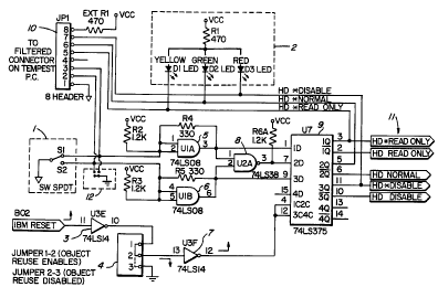
dotted lines in Fig. 3, Fig. 3 being a control circuit diagram
for switch 1. The external switch 1 consists of a SPDT switch
whose contacts are connected by leads to the internally
installed HPCCSD circuit card through an opening in the personal
computer case. The indicator display panel 2 consists of three
LEDs (one yellow, one green and the other red) which are also
connected by leads to the HPCCSD circuit board through openings
in the PC case. The switch 1 and indicator display panel 2 can
be mounted at the same location externally of the case. In the
particular circuit illustrated in Fig. 3, the yellow D1 LED of
display 2 is connected between a power supply Vcc and a
HD *READONLY line of the circuit card so that it, when
activated, will indicate when the HPCCSD circuit is in a read only
mode. The green LED D2 of display 2 is connected between the
power supply Vcc and a HD *NORMAL line to indicate when the
HPCCSD circuit is in a normal mode while the red LED D3 is
connected between supply Vcc and a HD *DISABLE line in order to
indicate when the HPCCSD circuit is in a disable mode. The
HD *READONLY, HD *NORMAL AND HD *DISABLE lines are connected to
output pins 3, 5 and 11, respectfully of integrated circuit
(IC) 9 whose input pins are connected to switch 1 via a number
of gates. Integrated circuit 9 is a device such as a Motorola
IC SN74LS375, commonly called a latch, 'which forms a latching
circuit.
The leads between switch 1 and the HPCCSD circuit board
as well as those between display panel 2 and that circuit board
- 15 -
~ 4 9 ~. ~ ~~ ~.
are also connected to a header 10 which is connected to a
filtered connector on any TEMPEST designed and approved PC in
order to prevent occurrence of any electromagnetic emissions
from the PC such as might be created by leads connected to those
externally mounted devices.
Output terminal S1 of switch 1 is connected to input
pins 1 and 2 of AND gate 5 whose output pin 3 is connected to
pin 1 of latching circuit 9. The input pins of AND gate 5 are
also connected to a Vcc source through a resistor R2. The arm
of switch 1 is connected to ground. Therefore, when the arm of
switch 1 is switched to a position connecting it to terminal S1,
it connects a ground to inputs of AND gate 5 causing those
inputs to go low with a signal from output pin 3 of AND gate 5
being applied to pin 1 of latching circuit 9. The output pin 3
of AND gate 5 is connected to its inputs via resistor R4 and to
the input pin 1 of NAND gate 8 whose output pin 3 is connected
to pin 7 of latch 9. Resistors R2 and 1~4 act to form a passive
debounce circuit to eliminate unwanted noise generated at
terminal S1 of the switch 1. The other input pin 2 of NAND gate
8 is connected to the output pin 6 of AND gate 6 whose input
pins 4 and 5 are connected together and to the other output
terminal S2 of switch 1. The output terminal S2 is disconnected
with the switch being in the position shown in Fig. 3. The
input pins 4 and 5 of AND gate 6 are connected to its output pin
6 via a resistor R5 with that output pin of AND gate 6 being
connected to input pin 9 of latch 9. The input pins 4 and 5 of
AND gate 6 are also connected to a Vcc source via a resistor R3.
- 16 -
5
Resistors R3 and R5 form a passive debounce circuit similar to
that formed by resistors R2 and R4. Those resistors will also
ensure that the switch makes active only one of the following
modes : read only, normal or disable.
This circuit arrangement, with switch 1 connected to
its terminal S1 as shown in Fig. 3, will provide a signal to
inputs 1, 7 and 9 of latch 9 to activate the HD *READONLY and
HD READONLY lines in cable 11 which are connected to output
pins 3 and 2 of latch 9 provided that latch 9 is enabled, i.e.
provided that the object rer~se at latch control pins 4 and 12 of
latch 9 is disabled. This will immediately place the computer
into a read only mode and activate display LED D1 which is
connected to the HD *READONLY line of cable 11. When switch 1
is switched to connect terminal S2 to the input terminals of
AND gate 6, however, this will result in activation of
HD *DISABLE and HD DISABLE lines in cable 11 which are connected
to output pins 11 and 10 of latch 9. Tlzis will place the
computer in a write disable and read disable mode and activate LED D3,
which is connected to the HD *DISABLE lane, to indicate that the
computer is in a disable mode. It should be noted that an
asterisked name, such as HD *DISABLE, is the inverse signal of
the same non-asterisked name, i.e. HD D:CSABLE.
If the switch 1 is in a neutral position where neither
terminal Sl or S2 are connected to the HPCCSD circuit board,
latch 9 will activate the HD NORMAL line at pin 6 of latch 9 and
also activate a HD *NORMAL line at pin ~5 of latch 9 which is
- 17 -
2091~~~
connected to LED D2 indicator light. This will activate LED D2
to indicate that the computer is in a normal mode. An optional
connector 12 which can connect both terminals S1 and S2 of
switch 1 to ground will disable circuits on the HPCCSD circuit
card.
Latch control pins 4 and 12 of latch 9 are connected
via an inverter 7 to an object reuse three terminal connector 4 ,
inverter's 7 input being connected to a central connector of
connector 4. A computer "RESET" line i;s connected to an input
of inverter 3 whose output is connected to a first terminal of
the three terminal connector 4 while a 'third terminal of
connector 4 is connected to ground. An electrical jumper
(internal option link) connected between the centre terminal of
connector 4 to the third terminal (ground) will connect the
inverter 7 input to the ground and disable the object reuse feature.
The output of inverter 7 is connected to latch control pins 4
and 12 of latch 9 and will, under these conditions, enable
latch 9 which will allow any changes in switch 1 to change the
modes of the circuit (read only, normal or disable) immediately at the
outputs of latch 9. The removal of the jumper between the
centre and third terminal of connector ~~ and its insertion
between the first and second terminal wall result in the output
of inverter 3 being connected to the input of inverter 7 which
will enable the object reuse feature. The output of inverter 7,
under these conditions, will apply a signal to latch control
pins 4 and 12 of latch 9 to disable its operation so that any
- 18 -
~~~I~~.~
changes made to switch 1 will not immediately affect the mode of
the HPCCSD circuit. Therefore, any mode changes to the circuit
will only occur after a "reset" or computer activated reset of
the computer has taken place, i.e. after the computer is
rebooted. A "computer activated reset" includes any one of a
the following actions:
a. the reset button on a computer is activated to
cause reboot;
b. the control + alt + delete keys are simultaneously
depressed to cause reboot;
c. power is turned off and than on to reboot; or
d. reboot is effected by a software command to reset.
When a computer is "reset", a pulse will be applied at the input
of inverter 3. With the jumper being lcacated between the first
and second terminals of connector 4, that pulse will be inverted
by gate 3, then re-inverted by gate 7 to appear at latch control
pins 4 and 12 and enable latch 9. When latch 9 is enabled, the
data present at its input pins 1, 7 and 9 will be stored at
outputs 3, 5 and 11 of latch 9. The re:~et pulse will then
become non-active, thus disabling latch 9 from accepting and
storing any new data from its inputs 1, 7 or 9. This will
prevent any accidental changes in the switch 1 position from
changing the mode of operation of the circuit during its normal
operation.
The interconnection of the HPC<:SD circuit board between
disk drive controller cable 28 and the cable 29 which is
connected to disk drives along with connections to the
- 19 -
2a9~.W.~
HD *DISABLE, HD *READONLY and HD READON:LY lines of cable 11 are
illustrated in Fig. 4. The HD *DISABLE line in cable 11 from
pin 11 of latch 9 (Fig. 3) is connected to a first input of each
of the NAND gates 18 and 19 of the HPCCSD circuit card. The
*DRIVE SEL 1 line (J1-26) from the disk drive controller cable
28 is connected through an inverter 13 on the circuit card to a
second input pin 2 of NAND gate 18 whose output pin 3 is
connected to the *DRIVE SEL 1 line (J2-26) of cable 29. A
signal on *DRIVE SEL 1 line from the drive controller will
normally travel through inverter 13 and NAND gate 18, provided
that no signal exists at pin 1 of gate :L8, to the *DRIVE SEL 1
line of cable 29 to select a first disk DRIVE #1 of the computer
and place that drive on standby. Howev~ar, a signal from the
HD *DISABLE line on input pin 1 of NAND gate 18 will disable
that gate when a signal appears on its :input pin 2 and block
transmission of any drive select signal to disk DRIVE #1 which
will prevent that drive from being selected or operated. This
will occur when switch 1 (Fig. 1) is in a position where
terminal S2 is contacted by the switch <~rm and will place the
computer into a mode in which nothing can be "written into" or
"read from" disk DRIVE #1.
In a similar manner, the *DRIVI~ SEL 2 line (J1-28) from
the drive controller cable 28 is conneci~ed through inverter 14
and NAND gate 19, provided no signal exists at pin 4 of gate 19,
to the *DRIVE SEL 2 of cable 29 to sele<a a second disk DRIVE #2
of the computer and place it on standby., This will allow data
to be "recorded on" or "read from" the :second disk when a signal
- 20 -
~~~~.~d)~:
is on the *WRITE GATE (J2-6) line of cable 29. However, a
signal from the HD *DISABLE line of cable 11 on input pin 4 of
NAND gate 19 will block transmission of any drive select signal
to disk DRIVE #2 and will prevent that drive from being
selected. This will place the computer into a mode in which
nothing can be "written into" or "read :from" the second disk
DRIVE #2. Since the HD *DISABLE line o:f cable 11 is connected
to a first input of both NAND gates 18 and 19 in the circuit
illustrated in Fig. 4, a signal on that HD *DISABLE line will
prevent either drive from being selected. In this mode, no data
can be "written into" or "read from" either of the disk drives.
However, if the HD *DISABLE line was on:Ly connected to one of
the NAND gates 18 or 19 on the circuit card, then only that one
drive associated with the NAND gate connected to the HD *DISABLE
line would be disabled by a signal on that line. Therefore,
depending on the circuit card connections (internal links),
either one of the disk drives could be placed in a disabled mode
by switch 1 where nothing can be "written into" or "read from"
that disk or both drives could be disabled as illustrated in the
circuit of Fig. 4.
The HD *READONLY line of cable 11 is connected to a
first input pin 9 of NAND gate 20 as well as to a second input
pin 10 of NAND gate 21. The *WRITE GATh line (J1-6) of disk
drive controller cable 28 is connected i:hrough inverter 15 to
the other input pin 10 of NAND gate 20 whose output is connected
to the *WRITE GATE line (J2-6) of cable 29. When no signal is
on the HD *READONLY line of cable 11 and pin 9 of NAND gate 20,
- 21 -
2Q9I ~~:~
then a signal on the *WRITE GATE (J1-6) line of cable 28 will
travel through inverter 15 and NAND gate 20 to the *WRITE GATE
line (J2-6) of cable 29. This will allow data to be recorded on
either one of the disk drives depending on which drive has been
selected and placed an "standby". However, when a signal is
present on the HD *READONLY line of cable 11 and applied to
input pin 9 of NAND gate 20, this will disable that gate on the
occurrence of a *WRITE GATE signal at pin 10 of gate 20 and
block that *WRITE GATE signal from travelling to line J2-6 of
cable 29. This will prevent any data from being recorded on
either disk and place the computer into a read only mode which will
occur when the switch 1 is switched to its terminal S1. This
will also disable the "WRITE FAULT" line since that line from
J2-12 of cable 29 passes through an inverter 23 to an input
pin 9 of NAND gate 21 whose other input pin 10 is connected to
the HD *READONLY line, a signal on both of those inputs disable
gate 21 and block any *WRITE FAULT signal from cable 29. The
inputs of inverters 13, 14, 15 and 23 a:re connected to a Vcc
supply by resistors R6, R7, R8 and R9, :respectively.
The *WRITE GATE line (J1-6) of cable 28 is also
connected via inverter 15 to input pin !5 of NAND gate 17 whose
other input pin 4 is connected to the H17 READONLY line of
cable 11. The NAND gate 17 will supply an output signal on
pin 6 when a signal appears from inverter 15 in the *WRITE GATE
line and the HD READONLY line. This oui~put signal is applied to
pin 2 of pulse stretcher circuit 24 which, if enabled, will
generate a signal on pin 3 to NAND gate 26 to activate buzzer 27
- 22 -
20~~. ~ ~I
from output pin 11 of NAND gate 26. The pulse stretcher circuit
24 will provide a long pulse out at its pin 3 when a short pulse
is applied at its input pin 2. Circuit 24 may be a device such
as a National Semiconductor LM555, commonly called a one-shot
timer. That short pulse would originate at the output pin 6 of
NAND 17 when a signal appears on the *W:RITE GATE line of cable
28 and the HD READONLY line. This arrangement will provide an
audio indication of a write attempt whenever a signal appears on
the *WRITE GATE line provided pulse stretcher circuit 24 is
enabled. However, pulse stretcher circuit 24 is provided with a
reset pin 4 connected to a central terminal of a three terminal
connector 25 which has a first terminal connected to a Vcc
supply and a third terminal connected t~o ground. A jumper
(internal option link) connected between the central terminal of
connector 25 and its first terminal will connect the Vcc supply
to pin 4 of pulse stretcher circuit 24 to enable it and allow
the buzzer to operate when a *WRITE GATE signal appears and with
the HPCCSD circuit being set in a read only mode. However, if the
jumper is removed from the first and central terminal of
connector 25 and placed between the central terminal and third
terminal of the connector, this will connect reset pin 4 of
pulse stretcher circuit 24 to ground, disabling the pulse
stretcher circuit 24 and preventing the buzzer from operating
when an output from inverter 15 is creamed by a signal on the
*WRITE GATE line of cable 28. This results in no audio signal
being provided when an attempt is made to write data on a disk
in a read only or disable mode.
- 23 -
~~9I ~ ~.~
A signal from inverter 15 in t:he *WRITE GATE line of
cable 28 is also applied to a first terminal of a three terminal
connector 16 whose central terminal is connected to input pin 13
of NAND gate 22, the third terminal of connector 16 being
connected to ground. Input pin 12 of N.AND gate 22 is connected
to the HD READONLY line of cable 11 with the output at pin 11 of
NAND gate 22 being connected to the *WRITE FAULT line of
cable 28. A jumper (internal option link) between the central
terminal of connector 16 and its third terminal will connect
input pin 13 of NAND 22 to ground and prevent any output signal
from appearing at pin 11 of NAND gate 22. A signal on the
HD *READONLY line of cable 11 applied t~o input pin 10 of NAND
gate 21 will disable NAND gate 21 and prevent any *WRITE FAULT
signal from the disk drive cable 29 reaching the disk drive
controller cable 28. This arrangement, with a jumper between
the central and third terminal of conne~~tor 16 and the
HD *READONLY line activated, will completely disable the *WRITE
FAULT 1 ine of the computer and place it in a Write Fault Disabled
mode. However, during normal operation, with no signal on the
HD *READONLY line to NAND gate 21, a write fault signal on the
*WRITE FAULT line (J2-12) of cable 29 wall travel through
inverter 23 and NAND gate 21 to cable 28 and provide a write
fault indication to the computer. This will provide, under a
normal operation mode, a "write fault" indication to the computer
whenever a disk drive cannot accept the data sent to it and
indicate that the data was not written <~s requested.
- 24 -
2~9~. ~~~~
Removing the jumper between the central and third
(ground) terminals of connector 16 and placing that jumper
between the connector's 16 first and central terminals will
connect input pin 13 of NAND gate 22 to the output of
inverter 15 in the *WRITE GATE line from cable 28. This will
place the HPCCSD circuit in a Write Fault Enabled mode. In this
latter mode, any signal on the *WRITE GATE line will be applied
through inverter 15 to input pin 13 of 1~1AND gate 22. This, with
the HD *READONLY line activated and app:Lying a signal to pin 12
of NAND gate 22, will result in a signa:L at output pin 11 of
NAND gate 22 being applied the *WRITE Fi4ULT line of cable 28.
In this mode, any *WRITE GATE signal from cable 28 will cause
NAND gate 22 to simulate a "write fault"' signal on the *WRITE
FAULT line (J1-12) to the computer. Therefore, this arrangement
with the HPCCSD circuit in a "read only"' mode will result in
placing the HPCCSD circuit in a Write Fault Enabled mode where any
signal on the *WRITE GATE line will simulate a "write fault"
signal to the computer to indicate that no data was recorded on
a disk as requested and that a write request was not completed.
The three terminal connectors 4 (Fig. 3), 16 and 25
(Fig. 4) are all located internally on the HPCCSD circuit board
and their associated jumpers (internal option links) between two
terminal of each connector can be set in desired configurations
before the circuit board is installed in the computer. Those
jumpers are considered as being selectable "internal option
links" for the HPCCSD circuit.
- 25 -
The HPCCSD circuit as described, provides a number of
different functions or modes which can be selected at will by
installing jumpers between appropriate terminals of the three
terminal connectors and by activation o:E the externally mounted
switch. The types of modes that can be selected are listed
below:
1. Mode selection Lexternal switch
(a) Disk normal - Allows normal operation of the hard
disk.
l0 (b) Disk read only - Allows only read attempts to the
hard disk.J All write attempts are
disabled.
(c) Disk disable - Disallows <~11 read and write
attempts to the hard disk. The
hard disk .is disabled.
or
Mode selection (internal link
(a) Disk normal - Allows normal operation of the hard
disk.
20 (b) Disk read only - Allows only read attempts to the
hard disk. All write attempts are
disabled.
(c) Disk disable - Disallows all read and write
attempts to the hard disk. The
hard disk is disabled.
- 26 -
~~~~ ~Q~
2. Object reuse linternal link
(a) Object reuse enabled - Provides object reuse protection.
All option changes will not take
affect until after a reset of the
computer.
(b) Object reuse disabled - Disables object reuse protection.
All option changes will take affect
immediately after being set on
option switches.
3. Drive activated internal switch)
(a) Drive 1 protected - Provides tlhe selected mode of
protection to hard drive 1.
(b) Drive 2 protected - Provides the selected mode of
protection to hard drive 2.
(c) Drive 1/2 protected - Provides the selected mode of
protection to hard drive 1 and
drive 2.
4. Write fault indicator (internal swiitch)
(a) Write fault enabled - Provides an indication to computer
operating :system that write did not
occur.
(b) Write fault disabled - Disables indication to computer
operating system that write did not
occur.
5. Write attempt indicator internal switch
(a) Write audible indicator
enabled. - Provides an audible indicator to
operator that a write was
attempted.
(b) Write audible indicator
disabled - Disables audible indicator to
operator that a write was
attempted.
- 27 -
2~9.I ~ ~~
Various modifications may be made to the preferred
embodiments without departing from the s>pirit and scope of the
invention as defined in the appended claims. For instance,
although the descriptions of the preferred embodiments have
generally been directed to hard disk (HD) drives, this HPCCSD
circuit could be used for floppy disk drives or any other type
of data storage devices located in a PC. Furthermore, although
the switch has been described as an externally mounted switch,
the switch could be internally mounted which would prevent easy
access to it by unauthorized users. The switch could also be
provided with a keylock and may be placed at a location which is
separated from the computer along with the indicator display.
- 28 -