Note: Descriptions are shown in the official language in which they were submitted.
2091~35
PATCH PLUG FOR CROSS-CONNECT EQUIPMENT
Technical Field
This invention relates to an electric~l conn~ctQr, and more particularly to
an el~-ctric~l plug having reduced crosstaLk coupling between conductor-pairs within
5 the plug and belwæll plugs.
Ba~ of the Invention
Information flow has increased subst~nt~ y in recent years, and
- networks have evolved to accommodate not only a greater number of users but also
higher data rates. An example of a relatively high speed network is the subject of
10 ANSMEEE Standard 802.5 which provides a description of the peer-to-peer protocol
procedures that are defined for the transfer of information and control betwæn any
pair of Data Link Layer service access points on a 4 Mbitls Local Area Network with
token ring access. At such data rates, however, wiring paths themselves become
a"tellllac that both broadcast and receive electrom~n~tic radiadon. Signal coupling
15 (crosstalk) between dirre~ pairs of wires is a source of interference that degrades
the ability to process incoming signals. This is manifested qu~ntit~ffvely as
decreased signal-to-noise ratio and, nltim~tely~ as increased error rate. Accordingly,
crosstalk becomes an increasingly significant concern in electrical equipment design
as the frequency of interfering signals is increased.
Crosstalk occurs not only in the cables that carry the data signals over
long distances, but also in the connectors that are used in cross-connect panels.
ANSMEEE Standard 802.5 discloses a Medium Interface Connector having
acceptable crosstalk rejection at the frequencies of interest. This Connector features
four signal contacts with a ground contact, and is hermaphroditic in design so that
25 two i~e.ntic~l units will mate when oriented 180 degrees with respect to each other.
This Connector is available as IBM Part No.8310574 or as Anixter Part No. 075849.
CrosstaLk rejection appears to result from short connector paths, ground shields, and
the selection of particular terminals for each wire-pair. As might be expected, such
connector arrangements are relatively expensive and represent a departure from
30 conventional interconnection hardware. For example, in commercial building
applications, large bundles of wire-pairs t~rmin~te in elçctric~l panels compri.~ing
linear arrays of individual connectors such as AT&T's 110-type insulation-
displacement connectors (IDC). Each IDC accommodates a single wire presæd
between its opposing contact fingers, and is so compact that many can fit into a small
Z09153~
-
- 2 -
area One bundle may come from a telephone central offic,e while another bundle
comes from telephone equipment within the building. Intel~omlecting particular
wires from one bundle with particular wires from another bundle is accompli~hed
with a p~tc!-col~ compri~in.~ a cord with a plug (patch plug) att~chPd to each end.
5 The cord includes one or more wire-pairs within a plastic jacket. The patch plugs
include a number of contact blades that are designed to be pressed into an equalnumber of IDCs within an array thereof. While the 110-type IDCs have become
extremely popular because of their cost and size, the plugs used to make electrical
connection with them suffer from excessive crosstalk at high frequencies. In
10 particular, EIA/TIA Commercial Building Standards specify a maximum crosstalk at
frequencies of 16-100 MHz. In order to meet end-to-end crosstalk requirement~, the
plugs thrmselves can only contribute a fraction of the total allowable crosstalkbetween wire-pairs.
Accordingly, it is desirable to design a patch plug having reduced
15 crosstalk belween collductor-pairs within the patch plug and between ~dj~ent patch
plugs.
Summary of the Invenffon
In accor~ance with the invention, a plug for ir~terconnecting a pair of
wires at its input with a pair of insulation displacement connectors (IDC) at its
20 output is improved. The plug compri.~es a ~ ectric housing which includes a pair of
non-in~ul~ted conductors that cross over and are spaced-apart from each other. Each
conductor compri.~es a generally flat blade portion for making contact with the IDC
at one end, and means for making electrical contact with a wire at the other.
In illustrative embodiments of the invention, the means for making
25 electrical connection at the other end of each conductor compri~es an insulation
displ~ce.ment connector. In one illustrative embodiment, the conductors are
ide~tir-~l, but are reverse-mounted in the dielectric housing.
Brief Description of ~e Drawin~
The invention and its mode of operation will be more clearly understood
30 from the following detailed description when read with the appended drawing in
which:
FIG. 1 discloses a cross-connect panel coml-ri.sing an array of in.~ tion
~ispl~remrnt connectors~ one end of which termin~tes building cables while the
other end is adapted to be interconnected with patch plugs constructed in accordance
35 with the invention;
2091535
- 3 -
FIG. 2 discloses an exploded pe,speclive view of a prior art patch plug;
FIG. 3 discloses an exploded pe.rspective view of a 3-pair patch plug
~e~igll.od in accordance with the present invention;
FIG. 4 discloses an exploded perspective view of a l-pair patch plug
S designed in accordance with the present invention;
FIG. S is a top view of a conductor for a patch plug in accordance with
the invention;
FIG. 6 is a side view of the conductor shown in FIG. S; and
FIG. 7 is an end view of the conductor shown in FIG. 6.
10 Detailed Descrip'don
Most communi~ation systems transmit and receive electrical signals
over wire-pairs rather than individual wires. Indeed, an electrical voltage is
me~ningless without a lt;felt;nce voltage - a person can't even get shocked unless
part of his body is in contact with a reference voltage. Accordingly, the use of a pair
15 of wires for electrical signal tr~nsmi~sion is merely the practice of bringing along the
reference voltage rather than relying on a local, fixed rerelc;nce such as earth ground.
Each wire in a wire-pair is capable of picking up electrical noise from noise sources
such as lightning, radio and TV stations. However, noise pickup is more likely from
nearby wires that run in the same general direction for long distances. This is known
20 as crosstalk. Nevertheless, so long as each wire picks up the same noise, the voltage
diLre~ ce between the wires remains the same and the diLre,~ ial signal is
unaffected. To assist each wire in picking up the same noise, the practice of twisting
wire-pairs in various p~ttçrn.~ emerged.
Modern commercial bllildinPs include an abundance of communications
25 equipment; not only are individual offices within the building equipped with
telephones and fax mA~hines, they now include computers that are in~lcollllectedwith other co,l,pulel~ through high speed communicadon networks. For ease of
admini~tration, appan~lus for interco~nectinp such eqllipment (with each other and
with outside nelwolhs) is centraliæd via interconnection (cross-connect) panels that
30 serve the entire building or at least large portions thereo Furthermore, increased
competition has caused co...paniçs to continl~lly improve their services by adding
new equipment and upgrading old equipment. Unfortunately, new/upgraded
eq~ )ment frequently operates at higher speeds (up to 100 Mbps) that exi.~ting
interconnection apparatus was not decigne~l to accommodate. AT&T's 110-type
35 cross-connect panels are a source of good news to building owners who already have
; ` 209153S
-4 -
such equipment in place because it meets EIAIT~ Commercial Building Standards
"Category 5" requirements. Indeed, the only missin~ link for full Category 5
compliance is a patch plug for m~ing connPctiQnS between cable ~e~ ...in~tions on
the cross-connect panel itself. Before procee~ing with the illlploved design of the
5 patch plug, a brief discussion of the the cross-coMect panel is useful.
FIG. 1 discloses a cross-coMect panel 10 co..~ ing an array of
insulation ~i~pl~cement connectors (lDC) 11, one end of which terminat~ps building
cable 60 while the other end is adapted to be interconnected with other IDCs on the
panel via patch plugs 30, 40. In addition to building cable 60, it is frequently10 npcps~ry to termin~te cable 70 from a location(s~ outside the building. Panel 10 is
shown having only a few connectors 11, although it is nnderstood that larger panels
exist and that many panels are co-located in a common bay. IDC 11 is a
collventional l lO-type connector that is commercially available from vendors such
as AT&T that are de.cignP-d to facilitate making mech~nic~l and electrical connection
15 to a wire -- particularly a wire that is surrounded by dielectric insulation. The IDC
includes a pair of opposing contact fingers that strip insulation from a wire that is
pressed belween the contact fingers so that an electri~l contact is made between the
wire and the IDC. The other end of IDC 11 is simil~rly constructed; however,
instead of pressing individual wires belween the contact fingers located therein, a
20 patchcord may be connPcted The patchcord compri.cP,s a cord 80 having a plug 30
on at least one end. As shown, plug 30 termin~tes a six-conductor cord 80 while
plug 40 termin~tes a two-conductor cord 90. Cables 80, 90 exist that are designPd
for minimum crosstaLk with nearby, adjacent cords -- even when they are paralleland close together for long ~ f~n~P~s. However, within patch plug 30, and between
25 patch plugs 40, crosstaLk between wire-pairs l~pl~senls a potential problem.
Prior Art
FIG. 2 discloses a prior art 4-conductor patch plug 20 which does not
meet EL~/TLA Category S requirements. The patch plug compri.ces a two-piece
dielectric housing 210, 230 which snaps together and captures four conductors 220-1
30 through 220-4. Each of these conductors incl~ldes an insulation displ~ement
connector 223 at one end for receiving individual wires from a cord; and a contact
blade221 attheotherendforinsertionintoIDC 11 (showninFIG. 1). Connecting
these two ends is body portion 222 which is shaped for insertion into the lower
dielect ic housing 210. It is noted thatindividual wire pairs are conventionally
209153~
-5 -
located a~j~cent to each other; which is to say that conductors 220-1, 220-2 areassociated with one wire-pair while conductors 220-3, 220-4 are associated with
another wire-pair. Crosstalk belween these pairs (caused particularly by conductors
220-2 and 220-3) is ~ cceplably high at data rates of 100 Mbps.
Lower housing member 210 is a plastic part that is molded, for eY~mple,
from LEXAN~ m~t~ri~l -- a polyc~l,onate resin. The lower housing member
includes four slots 211 therein for receiving conductors 220-1 through 220-4. The
conductors are factory-installed and firmly embedded in the lower housing. The
lower housing member is design~d such that patchcords of customized length can be
10 quickly assembled by technici~ns on site. Cords compri.cing a plurality of insulated
wires, surrounded by an in.eul~ting jacket (typically PVC), are prepared for
connection to the conductors within the lower housing member 210 by stripping
away a small portion of the jacket to expose the insulated wires -- illustratively,
24 gauge str~n~e~ copper wires. For ease of assembly, the insulated wires are placed
15 into the under.ei~e of upper housing member 230 which includes narrow ch~nnele for
holding the wires in fixed positions. Thereafter, the upper housing member 230 is
snapped onto the lower housing member 210 by pressing them together; and the
wires are collectively pressed/seated into the insulation displacement conn~ctors 223
of conductors 220-1 to 220-4. Additionally, hooks 231-232 and 212-215, that are
20 molded into the housing members, mate with latches (not shown) to hold the housing
members together. Openings 233-236 exist merely to simplify the molding tool
which forms latches in the upper housing member 230. Similar openings exist in the
bottom of the lower housing member 210 to simplify the molding tool which forms
hooks 212-215. Strain relief for the cord (not shown) is provided by block 216
25 which presses the cord tightly against the upper housing member to relieve strain
from the individual wire connections when the cord is pulled.
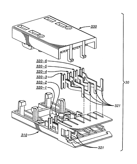
A Novel Patch Pll~g
FM. 3 discloses an exploded perspective view of a patch plug 30, in
accordance with the present invention, showing its assembly in detail. Patch plug 30
30 is similar in construction to the prior art patch plug 20 shown in FIG. 2. However,
the conductors are redesipne~ in such a manner that the crosstalk between adjacent
pairs of conductors is reduced by 8 to 9 dB over the prior art patch plug shown in
FIG. 2. Such an improvement is sufficient to meet EWTIA Category S
requirements. In accordance with the invention, crosstalk reduction (within a single
- 2091535
``~
- 6 -
patch plug and/or between pairs of patch plugs) is accomplished by crossing overconductor-pairs within the patch plug -- each conductor-pair being acsoci~tPd with
an input wire-pair, thereby improving capacitive balance. CrosstaLk reduction isfurther improved by minimi7ing the surface area of the contact blades 321. The
5 patch plug shown in FIG. 3 compri.ces upper housing mPmb~er 330 which is joined
together with lower housing member 310 in the manner disclosed in connection with
the prior art FIG. 2. The lower housing member is designed to contain the electrical
conductors and hold them aligned in prede~ermined positions. In accordance with
the present invention, conductor-pairs (320-1, 320-2), (320-3, 3204) and (320-5,10 320-6) are configured to subst~ntifllly reduce crosstaL~ between each other. Input
wires connect to the conductQrs using the insulation displ~cement connector at one
end of the conductor. These input wires usually come in pairs that are twisted
together to minimi7e crosstalk with nearby wires. The present invention adds a
controlled half twist to each input wire-pair which, heretofore, has not been
15 considered npces~ry. Furthermore, this is carried out in substantially the same
patch plug housing as the prior art so that it is fully compatible with existing cross-
connect panels. In the disclosed embodiment, the conductors are identical to each
other and are crossed by mounting ~dj~cent ones upside down. This provides the
advantage of reducing the number of different parts needed for the patch plug. It is
20 also possible to design two difrel~nl conductors in order to further minimi7e the
crosstaLk the conductor-pairs or improve structural integrity. Nevertheless, to
achieve the benefits of the present invention, these conductors must be paired
together and include a half twist between their input and output terrnin~l.c.
Whereas FIG. 3 discloses a patch plug having three conductor-pairs,
25 FIG. 4 discloses a patch plug 40, in accordance with the invention, having only one
conductor-pair. Such a plug is desirable because it is frequently mounted adjacent to
another patch plug as, for example, shown in FIG. 1. The patch plug shown in FIG.
4 includes upper housing member 430 which snaps into lower housing member 410.
Illustratively, hooks 412, 413 interconnect with latches 431, 433 during assembly.
30 This hook and latch assembly is the same as used in connection with FIG. 2 and 3,
but shown in greater detail here. Conductor-pair 320-1, 320-2 is shown already
inserted into the lower housing member 410. These con~uctors ~ermin~tP. in contact
blades 321 which are shown positioned for insertion into an IDC 11 of cross-connect
panel 10 (see FIG. 1). Strain relief block 416 cooperates with the interior of upper
35 housing member 430 to hold wires within the patch plug 40. The specific structure
209153~
of conductor 320 is disclosed in greater detail in FIG. 5-7.
FIG. 5 discloses a top view of conductor 320 in accordance with the
present invention. The conductor is fabricated from 0.016 inch-thick metal stocksuch as phosphor bronze and is appro~ ately 0.65 inches long.
FIG. 6 discloses a side view of the conductor shown in FIG. 5. Contact
blade 321 is the portion of conductor 320 that inserts into a pair of contact fingers of
IDC 11 shown in FIG. 1. The contact blade is, illustratively, 0.06 inches wide and
0.29 inches long.
FIG. 7 is an end view of the conductor shown in FIG. 6 showing the
10 design of the insulation displ~cement terminal portion of conductor 320. It is noted
that this particular design is reversible in that either contact fingers 323 or contact
fingers 324 may be used to receive wires pressed between them -- depending on
which pair of contact fingers is facing upward. When a pair of conductors 320 are
adjacent to each other, and mounted in opposite ori~nt~tions~ body portions 322 can
15 be arranged to cross over each other as required in the present invention.
Although a particular embodiment of the invention has been shown and
described, various modifications are possible within the spirit and scope of theinvention. In particular, it is understood that the actual shape of the conductors is a
matter of design choice, and that conductors that can be reversibly mounted are not
20 required.