Note: Descriptions are shown in the official language in which they were submitted.
WO92/Og~5 PCT/V591/0833-1
2091~9
RE~`n~ DI5PLAY ~ ~XOD OF ~FAC~E
FIELD OF THE INVENTION
The present invention pertains generally ~o signs
and displays. More particula:rly, the present invention
pertains to colored displays which can be used on
clothing tags, decals, packagi.ng material, and the like.
The present invention particularly, though not
exclusively, pertains to pxocess printed image displays
that have portions form~d on the displayed image to
enhance the effectiveness of the displayO
~0
BACKGROUND OF THE INVENTION
In the area of marketing, displays and designs have
been widely used on many products to increase the appeal
of the products and thereby make the products more
attracti~e to potential purchasers. For example,
fanciful displays and designs have been used on greeting
cards, packa~ing, decals, and the like to enhance the
appeal of these products.
Just one of the many types of displays which are
commonly used are displays which have a trnasparent
plastic substrate on which a designjis formed. As can be
readily appreciated, a large number of techniques exist
for forming the desired design on a plastic substrate.
Of particular importance to the present invention is the
technique known as process printing, of whicA
lithographic process printing and silk screen printing
are well-known species.
In its ~ost basic sense, process printing involves
forming an image on a substrate by depositing a large
numbar of very small, closely spaced colored dots onto
the substrate. Each of the dots has one of the four
primary colors, i.e. red, blue, yellow, or black. The
desired imaqe is formed on the substrate by particularly
depositing the variously colored dots onto the substrate
in a predetermined pattern, iOe. a predetermined color
WO ~2/09'~45 PCT / US~ ~ /0833'3
20~15~9
combination. The pattern or combination in which the
dots are deposited forms the desired image and also
establishes the colors o~ the image.
Typically, when an image is to be formed on a
plastic substrate for use as a clothing label, packaging,
and the like, the dots are translueent ink and are
process printed onto the substrate. The image thus
formed has a two-dimensional, flat appearanc~.
The present invention recognizes that the effect of
process printed displays can be enhanced by making
portions of the display appear to be metallic and shiny,
thereby giving the display a three-dimensional
appearance.
Accordingly, it is an object of the present
invention to provide a display which has a plastic
substrate and an image process printed thereon. It i5 a
further object of the present invention to provide a
display which has a process painted image with portions
of the image having a metallic, shiny appearance.
Another object of the present invention to provide a
display which has diverse applications and which is cost
effective to manufactureO
SUMMARY OF_THE INVENTION
A display which can be used as a greeting card,
clothing label, decal, packaging material, or the like
has c~ transparent plastic substrate, on which is formed
a colored image. Th~ image is formed by process printing
a large numbçr of relatively ~mall translucent colored
ink dots onto the substrate. In accordance with
well-known process printing techniques, e.g. lithographic
process printing and silk screen printing, the ink dots
are colored yellow, blue, and red, and are deposited onto
the substrate in a predetermined pattern to form the
desired colored image.
- - . .. . . . . . . .
W~92/09~5 PC~/~'S~l/08334
2~9:15~ -
Additionally, a stratum of opaque white ink may be
deposited over the ink dots which form preselected
portions of the image. Accordingly, those portions of
the i~age which have white ink deposited thereon are
substantially opaque to visible light. On the other
hand, those portions of the image which do not have white
ink deposited th~reon are substantially translucent to
visible light.
A reflective layer is deposited over the translucent
ink dots and white inX stratum which form the printed
image. This reflective layer is preferably a metalized
mylar sheet which i5 laminated to the substrate against
the ink dots and white ink layer. Alternatively, the
reflective layer can be a layer of metallic paint which
is deposited over the ink image onto the substrate by
spraying or by dipping the substrate in a container of
the paint. In any case, the effect of the reflective
layer is to reflect light which passes through the
transluc2nt portions of thP image, thereby gi~ing the
translucent portions of the image a shiny, metallic
appearance.
The novel featur~s of this invention, as well as the
invention itself, both as to its structure and its
operation, will be best understood from the accompanying
drawings, taken in conjunction with the accompanying
description, in which similar re~erence characters refer
to similar part~, and in which:
BRIEF DE$CRIPTION OF_THE DRAWINGS
Figure 1 is a front view of a display;
Figura 2 is a blown-up view of a portion of the
display shawn in Figure 1, showing the colored ink dots
which form the image on the display;
Fi~ure 3 is a cross-sectional view of the display as
; 35 seen along the line 3-3 in Figure l;
.: .j . .: , . . .
. .
W09?/09~5 PCT/US91/08334
2~91~9
Figure 4 is a cross-sectional view of the display as
seen along the line 4-4 in Figure 1; and
Figure 5 is a block diagram of the method of
manufacturing th2 display.
DESCRIPTION OF THE PREFERRED EMBODIM~ENT
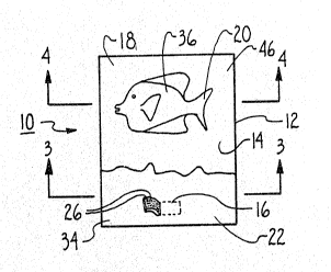
Referring initially to Figure 1, a display is shown
and generally designated 10. Display 10 includes a
transparent substrate 12. Substrate 12 ~an be a plastic
sheet or a glass pane, and furthermore can be tinted or
clear. In any event, suhstrate 12 must p~rmit the
passage of selected wavelengths of light in the visible
spectrum through substrate 12. Finally, substrate 12
al~o has a first surface 14 and a second surface ~6, best
shown in Figures 3 and 4.
Figure 1 also shows that substrate 12 can have any
desira~le image 18 printed thereon, such as the fish 20
jumping over the waves 22. As seen in cross-reference to
Figures 1, 3, and 4, image 18 is formed on substrate 12
by depositing a layer 24 of ink onto side 16 of substrata
12.
In accordance with the present invention, the ink
which is used for layer 24 is relatively viscous and is
curable within a relatiYely short period of tima (e.g.
six secQnds). ~ore specifically, it is pre~erred that
the inK be curable with ultraviolet (W) light.
Further, the ink should ~e relatively ~iscous, such as
. any of the enamel, epoxy and acrylic inks which are well
known in the art. Also, it is to be appreciated that the
: : 30 ink which forms predetermined portions of ink layer 24
may be translucent, whil~ the ink that ~orms other
predetarmined portions of ink layer 24 may be opaque.
Preferably the entlre ink layer 24 is translucent, for
: purposes to be shortly disclosed.
: 35 As~sho~wn in crossereference to Figures 1 and 2, the
. . .
:
WO92/~9q45 PCT/US')l/()~334
2~91~9
ink which forms layer 24 is deposited onto subs~rate 12
as a plurality of relatively small, closely spaced
colored ink dots 26. Ink dots 26 are deposited onto
substrate 12 by any sui~able mlethod of process printing,
for example lithographic process printing or silk screen
printing. As is well Xnown in the art, the dots 26 which
are printed onto substrate 12 are yellow, black, blue,
and red, although other colors may potentially be used.
Dots 26 are deposited onto substrate 12 in a
lo predetermined color combination which establishes both
the shape and color of image 18. It is to be appreciated
that the diameter 28 of the dots 26 is preferably small,
in order to establish a relatively high degree of
resolution of image 18. For example, when using the well
known silk screen process printing, a four hundred (400~
line per inch mesh will form dots 26 which have a
diameter 28 of approximately twenty five ten thousandths
.00025) 3f an inch. On the other hand, when using
lithographic process printing, the diameter 28 of dots 26
can be established to be as small as industrially useful.
Referring to Figures 3 and 4, a reflective layer 30
is shown deposited against ink layer 24. Furthermore,
Figure 4 shows that reflective layer 30 can be deposited
against portions of side 16 o~ substrate 12 which are not
covered by ink layer 24. It is to be understood,
however, that refl~ctive layer 30 need only be deposited
against selected portions of ink layer 24 that form
portions of image 1~ which are to appear metallic, e.g.
waves 22.
In the preferred embodiment, reflective layer 30 is
a sheet of ~etalized mylar which is laminated onto ink
layer 24 and side 16 o~ substrate 12. Alternatively,
re~Iective l.ayer 30 can be a layer of metallic paint or
ink:which is deposited onto ink layer 24 and substrate 12
by ~praying the metallic paint or ink onto ink layer 24
,:
:
WO92/09M5 2 0 91 ~ ~ 9 PCr/US9l/0X334
and subskrate 12. Reflective layer 30 can even be a
layer of metallic ink or paint which is deposited onto
ink layer 24 and substrate :12 by dipping side 16 of
substrate 12 (and, hence, ink layer 24) into a container
of the metallic paint or ink which is to form reflective
layer 30.
It will be recalled that the ink which forms ink
layer 24 is preferably translucent. Accordingly, light
can pass through ink layer 24 and be reflected back
10 through ink layer 24 by reflective layer 30 to give ink
layer 24 a metallic, shiny appearance. If desired,
however, light which passes through preselected portions
of ink layer 24 which are not to appear metallic may be
blocked from reflective layer 30 by for~ing the
preselected portions from opaque ink. Preferably,
however, the entire ink layer 24 i5 translu ent, and a
non-shiny opaque stratum 32, shown in Figure 4, is
deposited between the preselected portions of ink layer
24 which are not to appear metallic and reflective layer
30. In the pre~erred embodiment, opaque stratum 32 is a
~: layer of white ink which is process printed onto the
preselected portions of ink layer 24. Opaque stratum 32
~ of light to reflective layer 30 blocks the passage from
: those portions of ink layer 24 on which stratum 32 has
been deposited. Consequently, those preselected poritons
of ink l~yer 24 which have opaque stratum 32 deposited
there~n will not appear to be metallic. On the other
hand, those portions of ink layPr 24 which do not have
opat~ue stratum 32 deposited thereon will have a metallic
shiny appearance.
; To illustrate, as shown in cross-reference to
Figures 1 and 3, no opaque stratum 32 is deposited on the
portion 36 of ink layer 24, which forms fish 20 of image
18. Consequently, light can pass through portion 36 and
be reflected back through portion 36 by reflective layer
- .
.' .. . ; .: .: :
.., , .. :
.
W~2/09~5 PCT/US9l/0X3~
2~9 ~ ~89
30, which gives portion 36 (and, hence, fish 20) a
metallic, shiny appearanceO On the other hand, as seen
in cross-reference to Figures 1 and 4, opaque stratum 32
is deposited betwe~n preselected portion 34 (which forms
waves 22) of in~ layer 24 and reflective layer 30
Consequently, light which passes through portion 34 will
be ~locXed ~rom re~lective layer 0 by opaque stratum 32~
Thus, portion 34 ~and, hence, waves 22) will not appear
to be shiny or metallic.
METHOD OF MANUFACUTURE
In the method of manufacturing display 10, reference
is initially made to Figures 2 and 5. In accordance with
well known methods of process printing, including 5ilk
screening and lithographic proces~ printing, a large
number of relatively small, closely spaced colored dots
26 are deposited onto side 16 of substrate 12, shown i~
Figure 2, to form ink layer 24. This depositing step is
indicated at block 38 in Figure 5. Typically, each do~
26 will be a red, yellow, or blue translucent ink dot.
The variously colored dots 26 are deposited onto
substrate 12 in a predetermined combination, in
accordance with well known methods o~ process printing~
to form the image 18 shown in Figure 1.
Next, at block 40, a suitable opaque stratum 32, for
exampl~ opaque white ink, is deposited over preselected
portions of ink layer 24 ~e.g., portion 34) which form
those portions of image 18 (e.g., waves 22) that are no~
intended to appear metallic. No opaque stratum 32,
however, is deposited against those portions of ink layer
24 ~e.g., portion 36) which forms portions of image 1
(e.g., ~ish 20) that are to appear metallic. Stratum 32
may be sprayed, painted, or printed o~er portion 34 in
accordance with well known ink dsposition techniques.
Next, reflective layer 30 is deposited against
,~ .
`
- . ~ ':: ' '. ' ~ - . ' . ' ' : , ' .
.' . . : . ~: : : . : . ::
W0~2/094~S PCT/~S~l/08334
20~15~9
port.ions of ink layer 24 which ~orm portions of image la
that are intended to appear metallic. As seen in Figure
4, however, reflective layer 30 may additionally be
depssited against both ink layer 24 and portions of side
16 of substrate 12 which are not covered by ink layer 24.
In any case, reflective liayer 30 is preferably a
metalized mylar sheet. The mylar sheet which constitutes
reflective layer 30 can be laminated or glued onto 1nk
: layer 24 and substrate 12. l'his step is represented at
block 42a. On the other hand, reflective layar 30 may be
a layer of metallic paint which can b~ sprayed or printed
onto ink layer 24 and substrate 12, as indicated at block
42b in Figure 5. Layer 30 in the form of metallic paint
can even be deposited against ink layer 24 and side 16 of
: 15 substrate 12 by gently dipping side 16 of substrate 12
into a container (not shown) of the metallic paint. This
step is indicated in Figure 5 at block 42c. In any case,
display 10 is subsequently cured, for example by exposing
display 10 to ultraviolet light, at ~lock 44.
While a particular process printed image with
reflective coating as hsrein shown and disclosed in
detail is fully capable of obtaining the objects and
providing the advantages herein before stated, it is to
be understood that it is merely illustrative of the
present'y pre~erred embodiments of the invention and that
no limitations are intended to the details of
cons~ruction or design herein shown other than as
described in the appended claims.
,