Note: Descriptions are shown in the official language in which they were submitted.
2~221~
SEI 92-41
1 TITLE OF THE INVENTION
Semiconductor Device
BACKGROUND OF THE INVENTION
_ _
Field of the Invention
.... __
The present invention relates to a semiconductor
device having a high environmental resistance.
Related BacXground Art
Since the invention of a transistor in 1947, ICs and
LSIs are derived from transistors and semiconductor
techniques have been remarkably developed. In
particular, a silicon semiconductor technique has been
established, and various circuits are formed into ICs
which are used in a variety of applications. However,
elements have operational limitations caused by physical
properties of silicon. In some applications,
semiconductors except for silicon have been used.
For example, in the field of communications having a
very high frequency such as a microwave as in satellite
communication, the carrier mobility of ~ilicon is an
obstacle against the development of elements~ A
countermeasure against this problem is a method of
precisely micropatterning elements, but the
micropatt~rned element in turn poses another problem on
allowable power characteristics including heat
resistance. For this reason, GaAs having a high carrier
mobility has been used in place of silicon for the above
2~221~
SEI 92-41
1 applications. Similar prohlems are posed by high-speed
digital circuits (e~g., a supercomputer), and digital ICs
have been developed using GaAs as a semiconductor
material and are used in practice.
When silicon is used to form a bipolar transistor, a
largP current amplification factor, i.e., a high current
gain cannot be achieved by a simple pnp layer structure.
The collector breakdown voltaye cannot be increased by
this structure, either. For this reason, a specific
structure and circui~ arrangement have been implemented
so as to obtain a larger current amplification factor and
a higher collector breakdown voltage according to the
state-of-the-art techniques.
A material having a large band gap is preferably in
the above applications. A heterojunction bipolar
transistor is assumed as one of the devices which can take
over conventional silicon bipolar semiconductor devices.
Examples of the heterojunction bipolar transistor are
disclosed in Japanese Patent Laid-Open No. 62-216364,
62-2657762, 62-160760, and 62 159463. These examples are
transistors each utilizing a heterojunction formed
between silicon and silicon carbide. However, since
silicon is used as a material, drastic solutions to the
problems on a low breakdown voltage and a low resistance
to environment cannot be provided. Since materials such
as diamond and silicon carbide have large band gaps among
2~9221 ~
SEI 92-41
1 the currently available materials, good operations can be
expected in the above applicati.ons if these materials are
used. Extensive stud.ies have been made to develop a
better semiconductor material using these materials in
applications which cannot be coped with the silicon
semiconductor, as described in Japanese Patent Laid-Open
No. 64-55862 Eiled by the present applicant.
SUMMARY OF THE INVENTION
It is the first object of the present invention to
provide a semiconductor device (a transistor and an IC
using the transistor) wherein silicon carbicle is used to
form a collector region (first layer) and a base region
(second layer), and a material having a larger band gap
than that of silicon carbide of the base region is used to
form an emitter region (third layer), so that a
heterojunction is formed between the base and emitter
regions, and the base and emitter regions have a junction
of the same material, i.e., silicon carbide. In this
manner, only one heterojunction is formed to facilitate
formation of a good semiconductor layer.
The first and second layers are made of silicon
carbide layers having the same crystal structure to form
a homojunction between the base and emitter region,
thereby further facilitating formation of a good
semiconductor lay~r.
The material having a larger band gap than that of
2~2~l~
SEI 92-41
1 silicon carbide is diamond or BP~Nl2 (O ~ x s 1) (wherein
BP~Nl_~ can form a good layer having a lattice constant
almost equal to that of silicon carbide when x ~ 0.1).
If the base and collector regions are made of cubic
silicon carbide, hexagonal silicon carbide can be used
for the emitter region as a material having a larger band
gap than that of cubic silicon carbide.
Second, an SiC substrate is used as a substrate, and
the collector, emitter, and base regions are sequentially
1~ formed on the SiC substrate, so that a substrate having a
large area can be used to facilitate mass production of
devices.
In particular, assume that a layer (third layer)
using diamond or BP~N1_~ serves as the uppermost layer in
the emitter region. In this case, even if the third layer
does not have a uniform crystal structure on the entire
surface of the substrate, the third layer may partially
have a uniform crystal structure. This uni.form crystal
region can be used to arrange a device, thus providing an
advantage in that diamond or BPN need not be formed on a
large area. The third layer may have a polycrystalline
structure because a polycrystalline layer can be more
easily formed.
When cubic silicon carbide is used ~or the base and
collector regions, and hexagonal silicon carbide is used
for the emitter region, these semiconductor layers can be
2~2~
SEI 92-41
1 properly formed on the substrate because these layers and
the substrate are made of the same material. In addition,
either pnp or npn devices can be formed.
Since the bipolar transi~tor has a heterojunction
made of a semiconductor having a large band gap, a large
collector current can be obtained by a small base current
in accordance with the potential barrier formed by this
heterojunction.
The bipolar transistor has resistance to radiation
and can he properly operated at very high temperatures.
Since the band gap of the collector is large, the bipolar
transistor has a high collector breakdown voltage. This
allows formation of a good device as compared with a GaAs
device.
According to a method of manufacturing a
semiconductor device of the present invention, a
semiconductor device which can properly operate can be
manufactured.
When base and collector electrodes are self-aligned,
the base resistance and the base and collector
capacitances are reduced to obtain a high-performance
device.
The present invention will become more fully
understood from the detailed description given
hereinbelow and the accompanying drawings which are given
by way of illustration only, and thus are not to be
2~2~
SFI 92-41
1 considered as limiting the present invention.
Further scope of applicability of the present
invention will become apparent from the detailed
description given hereinafter. However, it should be
understood that the detailed description and specific
examples, while indicating preferred embodiments of the
invention, are given by way of illustration only, since
various changes and modifications within the spirit and
scope of the invention will become apparent to those
skilled in the art form this detailed description.
BRIEF DESCRIPTION OF THE DRAWINGS
_
Fig. 1 is a sectional view showing the structure oP
the first embodiment;
Figs. 2A to 2D are sectional views for explaining
the steps in manufacturing a transistor shown in Fig. 1;
Figs. 3A and 3B are band diagrams of the transistor
shown in Fig. 1;
Fi~. 4 is a sectional view showing a transistor
identical to that of Fig. 1 and having a self-aligned
structure;
Figs. 5A to 5D are sectional views for explaining
the steps in manufacturing the transistor shown in
Fig. 4;
Fig~ 6 is a sectional view showing the structure o~
the second embodiment;
Figs. 7A to 7D are sectional views for explaining
~3~D2~ ~ ~
SEI 92-41
1 the steps in manufacturing a transistor shown in Fig. 6;
Figs. 8A and BB are band diagrams of the transistor
shown in Fig. 6;
Fig. 9 is a sectional view showing a transistor
identical to that of Fig. 6 and having a self-a].igned
structure;
Figs. lOA to lOD are sectional views for explaining
the steps in manufacturing the transistor shown in
Fig. 6;
Fig. 11 is a sectional view showing the structure of
the third embodiment;
Figs. 12A to 12D are sectional views for explaining
the steps in manufacturing a transistor shown in Fig. 1~;
Figs. 13A and 13B are band diagrams of the
transistor shown in Fig. 11;
Fig. 14 is a sectional view showing a transistor
identical to that of Fig. 11 and having a self-aligned
structure;
Figs. 15A to 15D are sectional views for explaining
the steps in manufacturing ~he transistor shown in
Fig. 14;
Fig. 16 is a sectional view showing the structure o~
the fourth embodiment;
Figs. 17A to 17D are sectional views or explaining
the steps in manufacturing a transistor shown in Fig. 16;
Figs. 18A and 18B are band diagrams of the
2 ~
SEI 92-41
1 transistor shown in Fig. 16;
Fig. 19 is a sectional view showing a transistor
identical to that of Fig. 16 and having a self-aligned
structure; and
Figs. 20A to 20D are sectional views for explaining
the steps in manufacturing the transistor shown in
Fig. 19.
DETAILED DESCRIPTION OF THE PREFERRED EMBODIMENTS
Preferred embodiments of the present invention will
lo be described with reference to the accompanying drawings.
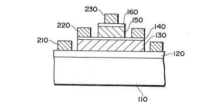
Fig. 1 shows the structure of a transistor according to an
embodiment. In this transistor, a p~-diamond layer 120, a`
p-diamond layer 130, an n~-SiC layer 140, a p-SiC layer
150, and a p+-SiC layer 160 are sequen~ially formed on a
nondoped diamond substrate 110. An emitter electrode
210, a base electrode 220, and a collector electrode 230
are electrically connected to the p+-diamond layer 120,
the n+-SiC layer 140, and the p+-SiC layer 160,
respectively. SiC is defined herein to have a cubic
crystal structure (3C-SiC or ~-SiC).
Pl P~, n, and n+ represent p- and n-type
semiconductor layers, and suffix "~" represent relatively
high impurity concentrations, respectively.
This transistor is manufactured by the following
steps.
The p+-diamond layer 120 and the p-type diamond layer
2~2~
SEI 92-41
1 130 are sequentially formed on the diamond substrate 110
by a microwave CVD method. ~t this time, the microwave
had a frequency of 2.45 GHz and an output power of 400 W,
and a source gas was a gas mixture of CH4/H2 at a ratio of
4 : 100. The growth conditions were a pressure of 500
Torr and a temperature of 600 to 900C. In this case, B2H~
is mixed in the source gas to dope B (boron~, and the
content of B is changed to form the p+-diamond layer 120
and the p-diamond layer 130. Thereafter, the n+-SiC layer
140, the p-SiC layer 150, and the p+-SiC layer 160 are
sequentially formed by a low-pressure CVD method. At
this time, the source gas was a gas mixture of C3H8/SiHCl2
at a mixing ratio of 1 : 2. ~2 was used as a carrier gas.
The growth conditions were a pressure of 200 Pa and a
temperature of 900 to 1,200C. In the growth of the
n+-SiC layer 140, PH3 is mixed in the source gas to dope P
(phosphorus). In growth of the p-SiC layer 150 and the
p+-SiC layer 160, B2HB is mi~ed in the source gas to dope
B, thereby growing the p-SiC layer 150 and the p+-SiC
layer 160 (Fig. 2A).
A mask is formed except for portions corresponding
to the collector and base regions. The p-SiC layer 150,
the p+-SiC layer 160, and the n+-SiC layer 140 are etched
by RIE (Reactive Ion Etching) (Fig. 2B). At this time, a
reaction gas is a gas mixture of CF~ ~ 2 (5%~- The
p~-diamond layer 130 is etched by RIBE (Reactive Ion Beam
2~21~
SEI 92-41
1Etching) using a gas mi~ture of Ar ~ N30 (20%) and a resist
on the nt-SiC layer 140 as a mask (Fig. 2C). The AlSi
emitter electrode 210, the TaSi base electrode 220, and
the Mo/Au collector electrode 230 are formed and wired
(Fig. 2D). In these steps, a sample was formed, and its
characteristics were measured. A current gain of 1,200
and a collector breakdQwn voltage of 20 V were obtained.
A good operation was performed even at a temperature of
300C.
10Aæ described above, the collector and base form a
homojunction, and the base and emitter form a
homojunction. Therefore, these layers can be formed with
high precision.
This transistor is a pnp transistor having a
heterojunction formed by p-type diamond and n-type SiC.
The p~-diamond layer 130 having a low carrier
concentration is formed together with the heterojunction
between the emitter and base. The p--SiC layer 150 having
a low carrier concentration is formed between the
collector and base. This transistor is operated using
holes as a majority carrier and is estimated to have a
band diagram shown in Fig. 3~. The band gap of the
emitter region is about 5.5 eV, the band gap of each of
the base and collector regions is about 2.2 eV, and a band
gap difference of about 3.3 eV is present between the
emitter and base.
SEI 92-41
1 Fig. 3B is a band diagram showing a state wherein the
transistor is DC-biased. Referring to Fig. 3B, electrons
are distributed in a Fermi-Dirac distribution at a
portion higher than the energy level of the lower end of
the conduction band of the base region (n+-SiC layer 140).
The Fermi-Dirac distribution of holes is obtained at a
portion higher than energy le~elg EV1 and EV2 of the upper
end of the valence band. The holes have a higher energy
in a downward direction. A DC bias operation will be
described with reference to Fig. 3B.
The transistor is forward-biased such that the
emitter has a positive voltage and the base has a negative`
voltage. The energy level of the base region is higher
than that of the emitter region. When forward biasing is
performed such that the collector has a negative voltage,
the energy level o~ the collector region becomes high.
Electrons as a minority carrier are injected from the
base, but only a small number of electrons having an
energy higher than the potential carrier of the emitter
region flow to the emitter. On the oth~r hand, the
potential barrier of the valence band is lowered by the
heterojunction, and the potential barrier is also lowered
by the bias. For this reason, most of the holes flow in
the collector region through the base region. Therefore,
a large collector current flows with a small base
current, thereby obtaining a large current amplification
11
2~22~ ~
SEI 92-41
1 factor
Since silicon carbicle has a larger band gap than Si
(Si: about 1.1 eV), the device can be properly operated
even at high temperatures although the band gap of SiC is
slightly narrowed at such high temperatures. In
addition, the device can be operated even at a high
collector voltage. This device is superior to a
state-of-the-art transistor by properly selecting
parameters such as a film thickness.
Since diamond having a high heat conductivity and a
low dielectric constant is used as the material for the
substrate, good heat dissipation properties can be
obtained. In addition, the stray capacitance of a wiring
layer can be reduced. These advantages are enhanced when
the device is used with a high power at a high frequency.
In particular, since the transistor shown in Fig. 1 has
the emitter on the substrate side, the emitters of a
plurality of transistors can be connected through the
p+-diamond layer 120 to advantageously arrange an ECL
(Emitter Coupled Logic) serving as a high-speed logic.
The above-mentioned transistor may be manufactured
to have a sQlf-aligned structure, as known in a compound
semiconductor (e.g., GaAs).
A compound semiconductor is used to form an HBT
manufactured by self-alignment using an insulating film
on a side wall, as described in Hayama et al., "Perfect
2~22~
SEI 92-41
1 Self-Aligned AlGaAs/GaAs HBT having ~lGaAs Protective
Film", the Instltute of Electronics and Information,
Technical Report ED-89-1~7 (1989j, PP. 68 - 69. This
structura is applied to the above-mentioned transistor,
as shown in ~ig. 4. ~igs. 5A to 5D show the steps in
manufacturing the transistor shown in Fig. 4.
The transistor may have a structure in which a
polyimide resin is used to form an insulating film, as
described in Moxizuka et al., "AlGaAs/GaAs ~BT's
Fabricated by a Self-Alignment Technology Using Polyimide
For Electrode Separation", IEEE Electron Device Letters,
EDL-9, 598 (1988), or an integrated structure, as
described in FAN-TZONG YUAN, et al., "The Development of
Heterojunction Integrated Injection Logic", IEEE
TRANSAC~ION ON ELECTRON DEVICE, Vol. 36, No. 10.,
October. Another example of such a transistor is
described in K. Naga~a et al., "Self-aligned AlGaAs/GaAs
HBT with low emi~ter resistance utilizing InGaAs cap
layer", IEEE Trans. Electron Devices, Vol. ED-35, PP. 2
7, 1988.
In the transistor shown in Fig. 4, the base
electrode 220 is self-alisned by an SiO2 protective film
170 formed on the side surfaces of th~ p-SiC layer 150 and
the p~-SiC layer 160. At the same time, the emitter
region is etched and the emitter electrode 210 is formQd,
using an SiO2 protective film 1~0 on the base electrode
~22~5
SEI 92-41
l Z20.
As in Fig. 2A, a p~-diamond layer 120, a p-diamond
layer 130, an n~--SiC layer 140, a p-SiC layer 150, and a
p~-SiC layer 160 are sequentially formed on a nondoped
diamond substrate 110 (Fig. 5~). Thereafter, the p--SiC
layer 150 and the p~-SiC layer 160 are eliminated using a
mask formed except for a portion serving as a collector
region, and a protective film 170 is formed (Fig. 5B). A
base electrode 220 and an SiO8 protective film 180 are
lo formed, and the p-diamond layer 130 and the n+-SiC layer
140 are etched using the base electrode 220 and the SiOz
protective film 180 as masks (Fig. 5C). An emitter
electrode 210 and a collector electrode 230 are then
formed (Fig. 5D). The same etching conditions as in the
above embodiment are used in this process, and the same
mask material and insulating material as in the above
references can be used.
Etching is performed using the pro~ective films 170
and 180, and the like to form the electrodes. For this
reason, the number of photomasks in the fabrication
process can be small, and the photolithographic process
including resist coating can be simplified. Error
factors caused by mask alignment can be reduced, and a
finer micropattern can be formed.
Various modifications of this embodiment can be
made.
~221~
SEI 92-41
1 For example, SiC is exemplified to have a cubic
cryskal structure. However, SiC may have a hexagonal
crystal structure (called 6~-SiC or a-Sic). 6H-SiC has a
band gap of 2.86 eV (band gap difference: 1.54 eV), and a
higher voltage than that required for 3C-SiC is required,
~ut heat resistance and collector breakdown voltage can
be improved.
Another embodiment of the present invention will be
described with reference to the accompanying drawings.
Fig. 6 shows the structure of a transistor according to
the second embodiment. In this transistor, a p+-SiC layer
160, a p-SiC layer 150, an n+-SiC layer 140, a p-diamond
layer 130, and a p+-diamond layer 120 are sequentially
formed on a nondoped SiC substrate 111. ~ collector
electrode 230, a base electrode ~2Q, and an emitter
electrode 210 are formed on and electrically connected to
the p~-SiC layer 160, the n+-SiC layer 140, and the
p+-diamond layer 120, respectively. SiC is defined herein
to have a cubic crystal structure (called 3C-SiC 20
~-sic ) .
This transistor is manufactured by the following
steps.
The p+-SiC layer 160, the p~SiC layer 150, and th
n+-SiC layer 140 are sequentially formed on the SiC
substrate 111 by a low-pressure CVD method. At this time,
a source gas was a gas mixture of C3H8/SiHC12 at a mixing
2~2~
SEI 92-41
1 ratio of 1 : 2, ~2 was used as a carrier gas, and the
growth conditions were a pressure o 200 Pa and a
temperature of 900 to 1,200C. In the growth of the
n~-SiC layer 140, PH3 i.s mixed in the source gas to dope P
(phosphorus). In the growth of the p-SiC layer 150 and
the p+-SiC layer 160, B2H~ is mixed in the souxce gas to
dope B (boron) to grow the p-SiC layer 150 and the p+-SiC
layer 160. Thereafter, the p-diamond layer 130 and the
p+-diamond layer 120 are sequentially formed by a
microwave CVD method. At this time, the microwave had a
frequency of 2.45 GHz and an output power of 400 W. A
source gas was a gas mixture of CH4/H2 at a mixing ratio of
4 : 100, and the growth conditions were a pressure of 500
Torr and a temperature of 600 to 900C. At this time, B2HU
is mixed in the source gas to dope B, and the content of
is changed to grow the p+-diamond layer 120 and the
p-diamond layer 130 (Fig. 7A).
The resultant structure is masked except for
portions serving as the emitter and base regions, and the
~0
diamond layers 120 and 130 are etched by RIBE (Reactive
Ion Beam Etching) using a gas mixture of Ar + N2O (20%)
(Fig. 7B). Thereafter, the p-SiC layer 150 and the n+-SiC
layer 140 are etched by RIE (Reactive Ion Etching) using a
resist on the diamond layers 120 and 130 as a mask
(Fig. 7C). At ~his ~ime, the reaction gas is a gas
mixture of CF4 + 2 (5%)- The AlSi emitter electrode 210,
16
SEI 92-41
1 the TaSi base electrode 220, and the Mo/Au collector
electrode 230 are formed and wired (Fig. 7D). A sample
was Eormed by these steps, and the characteristics oE the
sample were measured. The sample had a current gain of
1,200 and a collector breakdown voltage of 20 V. The
sample was properly operated even at a temperature of
300C.
This transistor is a pnp transistor having a
heterojunction formed by p-type diamond and n-type SiC.
The p-diamond layer 130 having a low carrier
concentration is formed together with the heterojunction
between the emitter and base. The p-SiC layer 150 having
a low carrier concentration is formed between the
collector and base. This transistor is operated using
holes as a majority carrier and is estimated to have a
band diagram shown in Fig. 8A. The band gap of-the
emitter region is about 5.5 eV, tha band gap o* each of
the base and collector regions is about 2.2 eV, and a band
gap difference of about 3.3 eV is present between the
emitter and base.
Fig. BB is a band diagram showing a state wherein the
transistor is DC-biased. Referring to Fig. 8B, electrons
are distributed in a Fermi-Dirac distribution at a
portion higher than the energy level of the lower end of
the conduction b~nd of the base region (n+-SiC layer 140).
The Fermi-Dirac distribution of holes is cbtained at a
2~9~2 1 .S
SEX 9~-41
1 portion higher than energy levels EVl and EV2 of the upper
end of the valence band. The holes have a higher energy
in a downward direction. A DC biased operation will be
described with reference to Fig. 8B.
The transistor is forward-biased such that the
emitter has a positive voltage and the base has a negative
voltage. The energy level of the base region is higher
than that of the emitter region. When forward biasing is
performed such tha~ the collector has a negative voltage,
the energy level o:E the collector region becomes high.
El~ctrons as a minority carrier are injected from the
base, but only a small numbar of electrons having an
energy higher than the potential carrier of the emitter
region flow to the emitter. On the other hand, the
potential barrier of the valence band is lowered by the
heterojunction, and the potential barrier is also lowered
by the bias. For this reason, most of the holes flow in
the collector region ~hrough the base region. Therefore,
a large collector current flows with a small base
current, ~hereby obtaining a large current amplification
factor. A band gap difference between SiC and Si of the
conventional structure is 1.1 eV, and a larger current
amplification factor than that of the conven~ional
structure can be obtained.
Since silicon carbide has a larger band gap than Si
(Si: about 1.1 eV), the device can be properly operated
18
2 2 ~ ~i
SEI 92-41
1 even at high temperatures although the band gap of SiC is
slightly narrowed at such high temperatures. In
addition, the device can be operated even at a high
collector voltage. This devlce i5 superlor to a
state-of-the-art transistor by properly selecting
parameters such as a film thickness.
Since SiC having a high heat conductivity and a low
dielectric constant is used as the material for the
substrate, good heat dissipation properties can be
obtained. In addition, the stray capacitance of a wiring
layer can be reduced. These advantages are Pnhanced when
the device is used with a high power at a high frequency.
In addition, since the SiC layers 160, 150, and 140 are
made of the same material, they can be properly formed. A
homojunction between the base and emitter is also an
advantage of this transistor.
Since the p-diamond layer 130 and the p+-diamond
layer 120 are formed as the uppermost layers, these
layers are finally formed in the fabrication process.
~0
For this reason~ in formation of these layers, a diamond
layer having a size (1 to 10 ~m) corresponding to the
emitter size can be selectively grown. For this reason,
the diamond layer need not be formed to have a large size,
and the manufacturing problems can be reduced.
The diamond layers 130 and 120 are preferably formed
by monocrystalline diamond, but may be formed by
19
2 !~ 9 2 2 ~ 5
SEI 92-41
1 polyorystalline diamond. In the latter case, although
the current injection efficiency and the current
amplification factor are reduced, fabrication can be
properly per~ormed. A polycrystalline diamond layer
having a relatively uniorm orientation, i.e., 95% or
more of the t110) planes was formed as a sample layer,
following the same procedures as in the above embodiment.
A transistor having a current gain of 250 was obtained
with this diamond layer.
Fig. 9 shows the self-aligned structure of the
transistor in Fig. 6.
In this transistor, a base electrode 220 is
self-aligned by an SiO2 protective film 170 formed on the
side wall of the diamond layers 130 and 120. At the same
time, an SiO2 protective film 180 on the base electrode
220 is used to etch the collector region and Eorm the
collector electrode 230. Figs. lOA to lOD show the steps
in manufacturing this transistor. These steps are
performed under the same etching conditions as in the
previous embodiment, and any other structure is the same
as that in Fig. 4.
Th~ p+-SiC layer 160, the p-SiC layer 150, and the
n~-SiC layer 140 are sequentially formed on the SiC
substrate 111 following the same procedures as in Fig. 7A
(Fig. 10~). The resultant structure is masked except for
a portion serving as an emitter region, and the p-diamond
~22~
SEI 92-41
l layer 130 and the p~-diamond layer 120 are formed by the
selective growth described above, thereby forming the
protective film 170 (Fig. 10~). The base electrode 220
and the SiO2 protective film 180 are formed, and the
n~-SiC layer 140, the p-SiC layer 150, and the p~-SiC
layer 160 are etched using the base electrode 220 and the
SiO2 protective film 180 as masks (Fig. lOC). The emitter
electrode 210 and the collector electrode 230 are formed
(Fig. lOD). The epitaxial growth is facilitated and the
lo product yield can be increased as compared with a case
wherein epitaxial growth is performed on the entire
surface. According to this fabrication method, a
transistor having a diamond layer having a size of 2 ~ma
had a very high current amplification factor, i.e., a
current gain of 900.
Since the protective films 170 and 180 and the like
are used as etching masks to form the electrodes, the
number of masks in the fabrication process can be
reduced, and the photolithographic process such as resist
coating can be simplified. Error factors caused by mask
alignment can be reduced, and a finer micropattern can be
formed.
Various modifications of this embodiment can be
made.
For example, SiC is exemplified to have a cubic
crystal structure. However, SiC may hav~ a hexagonal
2~9221~
SEI 92-41
1 crystal structure (called 6H-SiC or a-Sic). 6H-SiC has a
band gap of 2.86 eV (band gap difference: 1.54 eV), and a
higher volta~e than that required for 3C-SiC is required,
but heat resistance and collector breakdown can be
improved.
The third embodiment of the presen~ invention will
be described with reference to the accompanying drawings.
Fig. 11 shows the structure of a transistor according ko
the third embodiment. In this transistor, an p+-SiC layer
160, a p-SiC layer 150, an n+-SiC layer 140, a p-BP~N
layer 132, and a p+-BP~Nl~ layer 122 are sequentially
formed on a nondoped SiC substrate 111~ A collector
electrode 230, a base electrode 220, and an emitter
electrode 210 are formed on and electrically connected to
the p+-SiC layer 160, the n'-SiC layer 140, and the
p~-BP~N~ layer 122, respectively. "~" in BP~NlX is set to
0.1 so that the lattice constant of BP~NI~ becomes equal
to that of SiC. Since these lattice constants are equal
to each other, a fabrication advantage (i.e., the layers
132 and 122 can be properly formed) can be obtained as
compared with the fabrication of the transis~or shown in
Fig. 6. SiC is defined herein to have a cubic crystal
structure (3C-SiC or ~-SiC~.
This transistor is manufactured by the following
steps.
The p'-SiC layer 160, the p-SiC layer 150, and the
22
~221~
SEI 92-41
1 n+-SiC layer 140 are sequ~ntially formed on the SiC
substrate 111 by a low-pressure CVD method. At this time,
a source gas was a gas mixture of C3H8/SiHCl~ at a mixing
ratio of 1 : 2, H2 was used as a ~arrier gas, and the
growth conditions were a pressure of 200 Pa and a
temperature of 900 to 1,200DC. In the growth of the
n+-SiC layer 140, PH3 is mixed in the source gas to dope P
(phosphorus). In the growth of the p-SiC layer 150 and
the p+-SiC layer 160, B2H~ is mixed in the source gas to
dope B (boron) to grow the p-SiC layer 150 and the p'-SiC
layer 160. Thereafter, the p-BP~Nl_~ layer 132 and the
p+-BP~Nl~ layer 122 are sequentially formed by a thermal
CVD method. At this time, a source gas wa~ a gas mixture
of B2H~ (e.g., 5%), PH3 (e.g., 5%), NH3, and H2. The layers
were grown at a temperature of 800 to 1,100C. At this
time, Zn is used as a p-type dopant, Zn(CH3)~ is mixed in
the source gas, and the content of Zn(CH3)3 is changed to
grow the p+-BP~Nl_~ layer 122 and the p-BP~Nl_~ layer 132
(Fig. 12A). To obtain n-type BPXNl~ layers, for example,
Si is used as a p-type dopant, and Si~4 iS mixed in the
source gas.
The resultant structure is masked except for
portions serving as the emitter and ~ase regions, and the
BP~Nl_~ layers 122 and 132 are etched by RIB~ (Reactive Ion
Beam Etching) using a gas mixture of Ar + N20 (20%) (Fig.
12B). Thereafter, the p-SiC layer 150 and the n+-SiC
~221~
SEI 92-41
1 layer 140 are etched by RIE (Reactive Ion Etching) using a
resist on the BP~NI~ layers 122 and 132 as a mask
(Fig. 12C). ~t this time, the reaction gas is a gas
mixture o~ CF4~t 02 (5%)- The AlSi emitter electrode 210,
the TaSi base electrode 220, and the Mo/Au collector
electrode 230 are ormed and wired (Fig. 12D).
This transistor is a pnp transistor having a
heterojunction formed by p-type BP~NlX and n-type SiC.
The same advantage as in Fig. 6 is obtained except that
the emitter consists of BP~Nl_~. The p-BP~Nl_~ layer 132
having a low carrier concentration is formed together
with the heterojunction between the emitter and base.
The p-SiC layer 150 having a low carrier concentration is
formed between the collector and base. This transistor
is operated using holes as a majority carrier and is
estimated to have a band diagram shown in Fig. 13A. The
band gap of the emitter region is about 3.0 eV, the band
gap o~ each of the base and collector regions is about 2.2
eV, and a band gap difference of about 0.8 eV is present
between the emitter and base.
Fig. 13B is a band diagram showing a state wherein
the transistor is DC-biased. Referring to Fig. 13B,
electrons are distributed in a Fermi-Dirac distribution
at a portion higher than the energy level of the lower end
of the conduction band of the base region (n+-SiC layer
140). The Fermi-Dirac distribution of holes is obtained
24
2~2~1~
SEI 92-41
1 at a portion higher than energy levels EV1 and EV2 of the
upper end of the valence band. The holes have a higher
energy in a downward direction. A DC bias operation will
be described with reference to Fig. 13B.
The transistor is forward-bi.ased such that the
emitter has a positive voltage and the base has a negative
voltage. ~he energy level of the base region is higher
than that o the emitter region. When forward biasing is
performed such that the collector has a negative voltage,
the energy level of the collector region becomes high.
Electrons as a minority carrier are injected from the
base, but only a small number of electrons having an
energy higher than the potential carrier of the emit~sr
region flow to the emitter. On the other hand, the
potential barrier of the valence band is lowered by the
heterojunction, and the potential barrier is also lowered
by the bias. For this reason, most of the holes flow in
the collector region through the base region. Therefore,
a larye collector current flows with a small base
current, thereby obtaining a large current gain.
Since the emitter, base, and collector reyions have
larg~ band gaps, the transistor of this embodiment can be
properly operated even at high temperatures although the
band gaps are slightly narrowed at such high
temperatures. In addition, the devica can be operated
even at a high collector voltage. This transistor of this
~2~ 5
SEI 92-41
1 embodiment is superior to a state-of-the-art transistor
by properly selecting parameters such as a film
thickness. In addition, since SiC having a high heat
conduct.ivity and a low dielectric constant is used as the
material for the substrate, good heat dissipation
properties can be obtained. These advantages are
enhanced when the device is used with a high power at a
high frequency.
Fig. 14 shows the self-aligned structure of the
transistor described above.
In this transistor, the base electrode 220 is
self-aligned by an SiO2 protective film 170 formed on the
side wall of the BPXNl~ layers 132 and 122. At the same
time, an SiO2 protective film 180 on the base electrode
220 is used to etch the collector region and form the
collector elec~rode 230. Figs. 15A to 15D show the steps
in manufacturing this transistor. The etching conditions
are the same as those in the previous embodiment, and any
other arrangement is the same as in Fig. 4.
The p+-SiC layer 160, the p-SiC layer 150, and the
n+-SiC layer 140 are sequentially formed on the SiC
substrate 111 following the same procedures as in
Fig. 12A (Fig. 15A). The resultant structure is masked
except for a portion serving as an emitter region, and the
p-BP~NI~ layer 132 and the p+-BP~NI~ layer 122 are formed
by the selective growth described above, thereby forming
26
~221~
SEI 92-41
1 the protective film 170 (Fig. l5B). The base electrode
220 and the SiO2 protective film 180 are formed, and the
n+-SiC layer 140, the p-SiC layer.150, and the p+-SiC
layer 160 are etched using ~he base electrode 220 and the
SiO~ protective film 180 as masks (Fig. 15C). The emitter
electrode 210 and the collector electrode 230 are ormed
(Fig. 15D). Epitaxial growth i5 facilitated and the
product yield can be increased as compared with a case
wherein epitaxial growth is performed on the entire
surface.
Since the protective films 170 and 180 and the like
are used as etching masks to form the electrodes, the
number of masks in the fabrication process can be
reduced, and the photolithographic process such as resist
coating can be simplified. Error factors caused by mask
alignment can be reduced, and a finer micropattern can be
formed.
Various modifications of this embodiment can be
made.
For example, SiC is exemplified to have a cubic
crystal structure. However, SiC may have a hexagonal
crystal structure (called 6H-SiC or a-Sic)O 6H-SiC has a
band gap of 2.86 eV, and a higher voltage than that
required for 3C-SiC is required, but heat resistance and
collector breakdown can be improved. ~n addition, a pnp
transistor is exemplified, but the type of dopant is
27
2~22~ 5
SEI 92-41
l changed to obtain an npn transistor. Furthermore, the
value of x in BP~Nl~ is changed to change the band gap.
The fourth embodiment of the present invention will
be described with reference to the accompanying drawings~
` Fig. 16 shows the structure of a transistor formed on a
cubic SîC (called 3C-SiC or ~-5iC) substrate. In this
transistor, a p+-SiC layer 160 having a cubic crystal
structure, a p~SiC layer 150 having a cubic crystal
structure, an n~-SiC layer 1~0 having a cubic crystal
lo structure, a p-SiC layer 131 having a hexagonal crystal
structure (called 6H-SiC or a-SiC), and a p~-SiC layer 121
having a hexagonal crystal structure are sequentially
formed on a nondoped SiC substrate 111. A collector
electrode 230, a base electrode 220, and an emitter
electrode 210 are formed on and electrically connected to
the p~-SiC layer 160, the n+-SiC layer 140, and the p+-SiC
layer 121, respectively. In order to distinguish the
cubic crystal from the hexagonal crystal, cubic SiC is
represented as 3CSiC, and hexagonal SiC i5 represented by
6HSiC.
This transistor is manuactured by the following
steps.
The p~-3CSiC layer 160, the p-3CSiC layer 150, and
the n+-3CSiC layer ~40 are sequentially formed on the
3CSiC substrate 111 by a low-pressure CVD method. At this
time, a source gas was a yas mixture of C3H8/SiHC12 at a
28
~22~ ~
SEI 92-41
1 ~ixing ratio oE 1 : 2, H2 was used as a carrier gas, and
the growth conditions were a pressure of 200 Pa and a
temperatur~ of 900 to 1,200C. In the growth of the
n'-3CSiC layer 140, PH3 is mixed in the source gas to dope
P (phosphorus). In the growth o~ the p-3CSiC layer 150
and the p+-3CSiC layer 160, B2H~ is mi~ed in the source gas
to dope B (boron) to grow the p-3CSiC layer 150 and the
p+-3CSiC layer 160. Thereafter, the p-6HSiC layer 131 and
the p+-6HSiC layer 121 are sequentially formed by a
thermal CVD method. At this time, the p-6HSiC layer 131
and the p+-6HSiC layer 121 are formed in the same manner
as in the p+-3CSiC layer 160 and the p-3CSiC layer 150
(Fig. 17A).
The r~sultant structure is masked except for
portions serving as the emit~er and base regions, and the
6HSiC layers 121 and 131 are etched by RIBE (Reactive.Ion
Beam Etching) using a gas mixture of Ar + N2O (20%) (Fig.
17B). Thereafter, the p-3CSiC l~yer 150 and the n~-3CSiC
layer 140 are etched by ~IE (Reactive Ion Etching) using a
resist on the 6HSiC layers 121 and 131 as a mask
(Fig. 17C). At this time, the reaction gas is a gas
mi~ture of CF4 + O2 (5~). The AlSi emitter electrode 210,
the TaSi base electrode 220, and the Mo/Au collector
electrode 230 are formed and wired (Fig. 17D).
This transistor is a pnp transistor having a
heterojunction formed by p-type 5HSiC and n-type 3CSiC.
29
2~221~
SEI 92-41
l The p-6HSiC layer 131 having a low carrier concentration
is formed together with the heterojunction between the
emitter and base. The p--3CSiC layer 150 having a lo~
carrier concentration is formed between the collector and
base. ~his transistor is operated using holes as a
majority carrier and is estimated to have a band di~gram
shown in Fig. 18A. The band gap of the emitter region is
about 2.88 eV, the band gap of each of the base and
collector regions is about 2.2 eV, and a band gap
difference of about 0.66 eV i5 present between the
emitter and base.
Fig. 18B is a band diagram showing a state wherein
the transistor is DC-biased. Referring to Fig. 18B,
electrons are distributed in a Fermi-Dirac distribution
at a portion higher than the energy level of the lower end
of the conduction band of the base region (n+--3CSiC layer
140). The Fermi-Dirac distribution of holes is obtained
at a portion higher than energy levels Evl and EV2 Of the
upper end of the valence band. The holes have a higher
energy in a downward direction. A DC biased operation
will be described with reference to Fig. 18B.
The transistor is forward-biased such that the
emitter has a positive voltage and the base has a negative
voltage. The energy level of the base region is higher
than that of the emitter region. When forward biasing is
performed such that the collector has a negative voltage,
2~2~15
SEI 92-41
1 the energy level of the collector region becomes high.
Electrons as a minority carrier are injected from the
base, but only a small number of electrons having an
energy higher than the potential carrier of the emitter
region flow to the emitter. On the other hand, the
potential barrier of the valence band is lowerad by the
heterojunction, and the potential barrier is also lowered
by the bias. For this reason, most of the holes flow in
the collector region through the base region. Therefore,
a large collector current flows with a small base
current, thereby obtaining a large current amplification
factor. Since the emitter, base, and collector regions
have large band gaps, the transistor of this embodimsnt
can be properly operated even at high temperatures
although the band gaps are slightly narrowed at such high
temperatures. In addition, the device can be operated
even at a high collector voltage. This transistor of this
embodiment is superior to a state-of-the-art transistor
by properly selecting parameters such as a film
2~
thic~ness. In addition, since 3CSiC having a high heat
conductivity and a low dielectric constant is used as the
material for the substrate, good heat dissipation
properties can be obtained. These advantages are
enhanced when the device is used with a high power at a
high frequency. In addition, a large substrate can be
used to advantageously facilitate mass production.
31
~221~
SEI 92-41
1 In particular, this tran~istor has a heterojunction
using a single material as SiC. For this reason, as
compared with other heterojunction transistors, extra
material~ are not required, and the fabrication process
can be facilitated. In addition, an npn transistor can be
manufactured in addition to the pnp txansistor, and the
compositlon of the dopant can be controlled. Therefore,
transistors having different impurity profiles can be
formed. Transistors having various characteristics can
be provided in a variety of applications.
Fig. 19 shows the self-aligned structure of the
transistor in Fig. 16.
In this transistor, the base electrode 220 is
self-aligned by an SiO2 protective film 170 formed on the
side wall of the 6HSiC layers 131 and 121. At the same
time, an SiO2 protective film 180 on the base electrode
220 is used to etch the collector region and form the
collector electrode 230. Figs. 20A to 20D show the steps
in manufacturing this transistor. These steps are
performed under the same etching conditions as in the
previous embodiment, and any other structure is the same
as that in Fig. 4.
The pt-3CSiC layer 160, the p-3CSiC lzyer 150, and
the n+-3CSiC layer 140 are sequentially formed on the
3CSiC substrate 111 following ~he same procedures as in
Fig. 17A (Fig. 20A). The resultant structure is masked
2~92~1~
SEI 92-41
1 except ~or a portion serving as an emitter region, and the
p-6HSiC layer 131 and the p+-6HSiC layer 121 are formed by
the selective growth described ~ove, thereby forming the
protective film 170 (Fig. 20B). The base electrode 220
and the SiO2 protective Eilm 180 are formed, and the
nt-3CSiC layer 1~0, the p-3CSiC layer 150, and the
p+-3CSiC layer 160 are etched using the base electrode 220
and the SiO2 protective film 180 as masks (Fig. 20C). The
emitter electrode 210 and the collector electrode 230 are
lo formed (Fig. 20D). Since the protective films 170 and 180
and the like are used as etching masks to form the
electrodes, the number of masks in the fabrication
process can be reduced, and the photolithographic process
such as resist coating can be simplified. Error factors
caused by mask alignment can be reduced, and a finer
micropattern can ~e formed.
Various modifications of this embodiment can be
made.
For example, the SiC substrate is exemplified to
have a cubic crystal structure. However, the SiC
substrate may have a hexagonal crystal structure. In
this case, the emit~er region (6HSiC layers 121 and 131),
the base region (3CSiC layer 140), and the collector
region (3CSiC layers 150 and 160) are formed in the order
named. The emitter region serves as a lower lay~r to
~acilitate wiring in an ECL (Emitter Coupled Logic).
2~221~
SEI 92-41
1 From the invention thuæ descrihed, it will be
obvious that the invention may be varied in many ways.
Such variations are not to be regarded as a departure from
the spirit and scope of the invention, and all such
modifications as would be obvious to one skilled in the
art are intended to be included within the æcope of the
following claims.