Note: Descriptions are shown in the official language in which they were submitted.
f~
~~~~~,~~
3930-011-2
TITLE OF THE INVENTION
IMPROVED, LOiV LOSS, ELECTRONIC BALLAST
BACTCGROUND OF THE INVENTION
Field of the Invention
The present invention relates to an electronic ballast
for starting and operating high intensity discharge (HID)
'lamps using a new, low energy loss circuit arrangement
connected across a common low voltage AC power source which
provides improved efficiency when contrasted with conventional
HID lamp ballasts.
Discussion of the Background
Prior art HID ballast circuit such as disclosed in U.S.
Patent No. 4,337,417 utilize transformers connected in series
to an input AC voltage source at one end and to an output
terminal of a HID lamp at the other end. Capacitors and
charging resistors as well as blocking diodes are utilized in
order to effect high voltage starting pulses for lamp
ignition. Ignition occurs when a capacitor is initially
charged to the peak voltage of the AC source during the
negative-half cycle of the source and then when the source
voltage goes negative the voltage of the first capacitor is
added to a second capacitor in order to provide a voltage of
twice the AC input source voltage. A transformer utilizes
discharge energy and applies a voltage pulse of sufficient
C~~ r;r ~ a A ~
_2_
;magnitude across a lamp. This type of prior art suffers from
a lack of efficiency because of energy loss in the circuit.
Most energy loss occurs in the transformers which generate
high heat losses. Thus there is critical need to more
efficiently start and operate HID lamps without the high
energy losses which are characteristic of the conventional
ballast circuits using a high loss element.
Other prior art devices have attempted to address this
high loss problem. One approach is the "lead ballast'° circuit
structure such as shown in U.S, Patent No. 3,710,184 wherein a
low energy circuit is used to cause an open circuit voltage
(OCVy for lamp ignition to be increased. This type of system
also has energy losses which cause.it to provide less than an
optimal solution.
Another approach is taken in the U.S. Patent No.
3,700,962 of 7Hunson which utilizes a low voltage high energy
source but which does not provide any measure of taking into
account the dynamic impedance of the discharge necessary with
HID lamps. That is, many discharge lamps have dynamic
specific needs which cannot be addressed by a single
application of a voltage or a single application of one single
specific amount of energy.
Thus there remains a need to more efficiently start and
operate HID lamps without the high energy losses which are
characteristic of conventional ballast circuits using a high
loss element. There is also a simultaneous need to operate
CA 02092236 2001-06-05
-3-
HID lamps using systems which are capable of taking into account
the dynamic impedance requirements for HID lamps without a
substantial loss of efficiency.
SUMMARY OF THE INVENTION
Accordingly, the present invention seeks to provide a low
loss capacitive ballast circuit which overcomes the drawbacks
associated with prior art devices.
Further, the present invention seeks to provide a low energy
loss circuit which is capable of providing energy pulses of
sufficient magnitude to efficiently start and operate the high
intensity discharge (HID) lamps.
Still further, the invention seeks to provide a ballast
circuit arrangement which uses a novel concept for processing
electrical energy from an AC source by providing a driving
voltage sufficient to cause the dynamic impedance of the lamps
to be power pulsed by a capacitively dictated energy pulse by
using a plurality of energy delivery loops to cause the lamp to
receive energy in stages.
Further still, the present invention seeks to provide a novel
circuitry which first provides a low energy sufficient to drive
down the resistance of a HID lamp from a high driving voltage
loop and subsequently delivers a larger energy pulse at a lower
voltage to operate the HID lamp having the lowered resistance.
Moreover, the invention seeks to provide multiple voltage
energy delivery loops each having different energy levels in
order to properly meet the various dynamic needs of high energy
discharge lamps.
The invention in one aspect provides an electronic ballast
circuit including a starting circuit and an operator circuit for
starting and operating a high intensity discharge lamp from a low
voltage AC power source. The operating circuit compresses first
circuit means for storing a first voltage at a first energy level
wherein the first circuit means provides an output to a high
intensity discharge lamp and wherein the first voltage at the
first energy level functions to lower an impedance of the lamp.
CA 02092236 2001-06-05
-4-
Second circuit means includes a second means for storing a second
voltage at a second energy level and providing an output pulse
at the second energy level to the lamp in order to operate the
lamp. Diode matrixing means is connected between the first and
second circuit means for causing the second energy level pulse
to bypass the first circuit means during a half-cycle operation
of the source and immediately following the lowering of the lamp
impedance during the half-cycle, wherein the first circuit means
for storing the first voltage and the second circuit means for
storing the second voltage are selected so that a value of the
first energy level is of the same order of magnitude as a value
of the second energy level.
Another aspect of the invention provides and electronic
valve circuit for a high intensity discharge lamp wherein the
circuit is driven by a low voltage AC source and wherein the
valve circuit includes a starter circuit and an operating
circuit. The operating circuit comprises a low energy, high
voltage means for providing a first low energy delivery loop for
lowering an impedance of the lamp, wherein the low energy high
voltage means is connected to the source and provides the first
energy delivery loop during a first half-cycle operation of the
source. A high energy, low voltage means provides a second high
energy delivery loop to the lamp subsequent to the first energy
loop and subsequent to the impedance lowering of the lamp and
which the high energy pulse operates the lamp. The high energy
loop has an energy value of the same order of magnitude as, but
greater than, an energy value of the low energy loop and wherein
the low energy loop and the high energy loop are both provided
subsequent to ignition by the starter circuit of the lamp.
Still further the invention comprehends a low loss low
voltage metal halide lamp ballast circuit, comprising a pulsed
starter circuit for igniting the lamp, a low voltage AC power
source, a low loss capacitive means connected to the power source
for increasing the voltage output of the power source and
controlling flow of at least two different levels of energy
CA 02092236 2001-06-05
-4A-
subsequent to the igniting of the lamp by the starting circuit
to provide operation of the lamp wherein the at least two levels
of energy are provided as a function of the dynamic impedance of
the lamp and wherein a value of each of the at least two levels
of energy is of the same order to magnitude as a value of another
one of the two levels of energy.
BRIEF DESCRIPTION OF THE DRAWINGS
The foregoing features and objects of the present invention
will become clearer upon the following detailed description of
the preferred embodiments where like numerals represent like
elements throughout the description.
Figure 1 is an illustration of the energy flow in a prior
art ballast circuit arrangement;
Figure 2 shows the energy flow in a low-loss capacitive
ballast circuit used in the system of the present invention;
Figure 3 shows a detailed arrangement of the capacitive
circuit connected between an AC voltage and the HID lamp
according to the present invention;
Figure 4 shows an alternate embodiment of the circuit
arrangement utilizing additional higher voltage low energy source
superimposed to ignite a high discharge lamp involving additional
charging energy loops connected in parallel with the AC source
input;
Figure 5 illustrates a lamp circuit utilizing the capacitive
circuit of the present invention modified for a T-8 fluorescent
lamp.
-5-
DETAILED DESCRIPTION OF TFiE PREFERRED EMBODIMENTS
Referring now to Figure 3 of the drawings, the ballast
circuit structure of the invention uses a low voltage AC input
source 2, connected between two symmetrical circuits. The
first circuit .includes the capacitor C~ and C3 with the diode
matrix D1 and D2 being connected across the capacitor C~ and to
one terminal of the capacitor C~. Capacitor C~ has the other
terminal connecaed to one input of the source 2 and the other
input of the source is connected to the junction between the
capacitor C, and the diode D2. The other half of the
symmetrical circuitry formed by capacitor CZ and C~ and diode
D3 and D4 are connected in the same manner. Terminals 15 and
16 designate the outputs of the symmetrical circuit with
terminal 15 being connected at the juncture between capacitor
C, and diode D1 and the terminal 16 being taken at the juncture
between the capacitor C, and the diode D4. The voltage formed
at terminals 15 and 16 constitutes the open-circuit voltage
(OCV) provided through an inductive reactor 3 which bridges
the input terminal 14 of the metal halide HID lamp 1.
The ballast circuit of Figure 3 is such that when a
voltage is applied from the source 2, the capacitor C, and CZ
are charged to a value equal to the peak voltage of the AC
source which is 170 volts (designated as E in Fig. 3) in the
case of a 120 volt AC source and the capacitors C~ and C4 are
charged to a value which is twice the peak value or 340 volts
(designated as 2D in Fig. 3). For purposes of the operation
a ~'
of a HID lamp, the capacitors C, and Cz are sized to be high
energy capacitors while the capacitors C3 and c; are sized to
be low energy capacitors. Thus, the capacitor C3 and C4 are
high voltage low energy capacitors while the capacitors C~ and
C~ are law voltage high energy capacitors. The lamp driving
energy which is necessary for ordinary operation of the lamp
is effectively placed on the high energy capacitor element Ct
'which dictates the amount by the sizing of the capacitor.
This energy is trapped until a next half cycle of the AC
source when, through the action of the diode matrix D1, D2,
this energy is passed on to the lamp. However, the passing on
to the lamp during a subsequent half cycle is not acccmplished
until the lamp 1 has its impedance lowered by the output from
the high voltage low energy source C3. After the low energy
high voltage source C3 pushes the lamp to its lower impedance
instantaneous state, it is able to receive the energy from the
high energy source Ct in order to operate the lamp. Thus,
there is a two-stage delivery system to the structure of
Figure 3. In a first stage the higher voltage low energy
source on the capacitor C3 pushes the lamp into a lower
impedance instantaneous state which enables the lower voltage
high energy source Ci to subsequently deliver its energy to the
discharge lamp impedance level in a second stage.
It is the diode matrixing shown in Figure 3 which allows
the low voltage high energy pulse from C, to bypass the higher
voltage lower energy source C~ as it delivers its high energy
~ c G ~i.
a
tJ t-J ~ C
-7-
pulse to the lamp load. The distribution of the various
energy magnitudes required for the first and second loops is
easily ratioed to meet the specific discharge lamp dynamic
needs. The symmetry set up by the C" C~ and D1 and D2
operation is of course mirrored in the C." CA and D3, D4
circuit.
In the embodiment of Figure 3, the source 2 is a 120 volt
~C source and the capacitors C~ and CZ are 22.5 microfarad
while the capacitors C3 and C4 are 4 microfarad. The lamp
being served is a 50 watt M.H. (Metal Halidej. The shown
inductor Ldc is 28 watt in the example of Figure 3. Of
course, the reactor Lde could be replaced with other
structures such as resistors or chokes or incandescent lamps.
Furthermore, the use of a SIDAC is anticipated as an alternate
embodiment. The important feature however is that the
circuitry of Figure 3 generates a OCV voltage of 4 x 170 = 680
volts and the arrangement of the capacitors and diodes
provides for the two-stage operation wherein the high voltage
low energy capacitors C3 and C4 pushes the lamp into a lower
impedance instantaneous state which therefore enables the low
voltage high energy source C~ and CZ to deliver its energy to
the discharge lamp impedance level. This is made possible
because of the diode matrixing D1-D2 and D3-D4.
The Figure 4 shows an alternate embodiment using the
superposition of an even higher voltage very low energy source
~ which may be used to ignite the lamp. As many voltage
6/~l fi~ Yt~~ o ~ i >
~J ~~ ~ ~ .;fry'-t~s'! C'
_g_
energy level sources as necessary can be easily added in order
to obtain the full dynamic impedance behavior demanded by the
particular lamp 1. In many instances, the low energy circuit
symmetry on either side of the AC source may not be necessary
for lamp ignition.
It is to be noted that the open circuit voltage (OCV) of
the embodiment of Figure 3 is equal to four times 170 or 6g0
;volts while the open circuit voltage (OCV) of the variation of
Figure 4 provides an open circuit voltage of six times 170 or
1,020 volts. With the structure of the embodiment of Figure 4
a resistor or incandescent lamp choke 61 may be used.
The Figure 4 embodiment for a particular discharge lamp
100 shows the utilization of a resistor or incandescent lamp
300 which may also be a choke or other structure appropriate
to required operation of the lamp. The capacitor Cs and the
capacitor C6 have a value of 0.1 microfarad when a 100 watt,
144 ohm resistor or incandescent lamp 300 is utilized in
conjunction with the discharge lamp 100. Thus, it can be seen
that the energy level is much lower than that of the Figure 3
embodiment. Consequently, the capacitors Cs and C6 in the
Figure 2 provide a superposition of an even higher voltage and
very low energy source to ignite the lamp. Once again, the
distribution of the various energy magnitudes can be easily
adjusted to meet the specific discharge lamp dynamic needs.
It must also be emphasized that as many voltage-energy level
sources as necessary can be added to the Figure 4 embodiment
A'~ '' ~ o ~ s~~~ ~j ~2
f:, ~. . r.,, <a
_g_
as is necessary to meet the full dynamic impedance behavior of
a particular lamp. It is also noted that the low energy
circuit symmetry on either side of the AC source 2 is not
necessary for lamp ignition in many lamp instances.
The superimposing of different energy levels from several
sources, each delivering their designed quantity of energy via
the diode matrix without losses or interference, provides the
;low loss flexible improved ballast circuit for the ignition
and the economic and efficient sustaining of HID lamps.
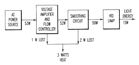
A comparison of the Figures 1 and 2 shows the improved
efficiency resulting from the system of Figure 3. In the
prior art which utilized a combination of a voltage amplifier
and a flow controller separately, there was a loss of 22 watts
of heat and a requirement beginning with a power source
providing 72 watts in order to provide the necessary 50 watt
input for the HID lamp. In contrast, the Figure 2 shows a
three watt heat loss when the system of Figure 3 is utilized.
Thus, there is only a requirement for a source of power of 53
watts in order to deliver the necessary 50 watts to the HID
lamp.
The circuit shown in Figure 5 embodies the capacitive
circuit of Figure 3 modified for a particular T-8 fluorescent
lamp circuit. The fluorescent lamp circuit includes the
filaments 51 and 52 and the preheating circuit constituted by
the TTC (positive temperature coefficient resistance) and the
RFC (radio frequency choke) 54 and 55, respectively. The
6~ r3 ', '
~~J t.~ Ld s-d (d ?JD
-L~
remainder of the lamp circuit includes a SIDAC 56 and a
starter capacitor 57 which in the particular example as a
value of 0.15 micro farads. The capacitor 57 is connected in
parallel with the SIDAC 56 which are in turn connected in
series with the starter resistor 58 having a value of 680K
ohms and being rated at 2 watts. The source used in the
particular example is a 120 volt source VAC but it could be a
.kaigher voltage such as 277 if the supply-lamp system requires
such a high voltage. The T-8 fluorescent lamp is a 32 watt
lamp and with such a structure as shown in the Figure 5 the
tapped choke 61 has a value of 0.2 henries and the capacitors
C1 and C2 have a value of 15 microfarads while the capacitors
C3 and C4 have a value of 1 microfarad.
These values for the capacitors C1, C2 and C3, C4 would
be only slightly larger in order to drive a 40 watt lamp. The
losses from such a circuit as shown in Figure 5 run between 1
and 2 watts and generate 3050 lumens or 90 system lumens-per-
~datt as compared to 53.5 L.P.W. for a standard F40CW T-12
single lamp ballast system and value of 63.5 lumens-per-watt
for a two lamp ballast system of the prior art.
The two component (low cost, small lamp preheating
circuit) (PTC and RFC) is used to provide a long lamp life,
high lumen maintenance, and -20'F starting which allows for
outdoor applications. A cold PTC (positive temperature
coefficient resistance) allows the proper preheating to take
place and then effectively drops out of the circuit as the PTC
,.;~ ~.~ ? ~ f~
-11-
resistance reaches high values. Subsequently, the low cost
three component ignitor (56, 57 and 58) steps in to ignite the
lamp and is then clamped off (de-energized) as the lamp comes
on.
This system for the T-8 fluorescent lamp provides a
tremendous improvement in performance efficiency especially in
high volume building lighting.
Obviously, numerous modifications and variations of the
present invention are possible in light of the above
teachings. It is therefore to be understood that within the
scope of the appended claims, the invention may be practiced
otherwise than as specifically described herein.