Note: Descriptions are shown in the official language in which they were submitted.
2092333
., 1 -
BUILT-IN SELF-TEST NETWORK
Technical Field
This invention relates to a network, and its method of operation, for
controlling the testing of two or more self-testing elements within a digital circuit.
S Back~round of the Invention
Modern digital circuits now incorporate ever larger arrays of circuit
elements (RAMs, ROMs CAMs, FIFOs and Random Logic blocks, for example) as
designers strive to provide increased circuit functionality. The increasing density of
modern digital circuits has greatly increased the difficulty of testing such circuits
10 with conventional external testing machines designed for this purpose.
Consequently, much effort has been devoted to designing individual circuit elements
with an ability to test themselves, that is, provide the elements with a Built-in Self-
Test (BIST) capability. Examples of circuit elements having BIST capability are
found in U.S. Patent No. 4,872,168, issued on October 3, 1989, and U.S. Patent
15 5,091,908, issued on February 25, 1992, both assigned to AT&T Bell Laboratories,
the present assignee.
The presence of individual circuit elements having BIST capability
within a Very Large Scale Integrated (VLSI) circuit has not, however, elimin~te~ the
difficulty of testing. The testing of a VLSI circuit incorporating a variety of BIST'd
20 elements, that is, elements having BIST capability, requires that an interface be
provided within the circuit to couple a control signal from a test controller to each
BIST'd element to initiate self-testing. In addition, the interface also must serve to
latch a test signature generated by each BIST'd element at the completion of testing
to allow subsequent transfer of the signature to the test controller.
One approach to providing such an interface for BIST'd RAM elements
is described in the paper "ASIC Implementation of Boundary-Scan and BIST" by
H. N. Scholz et al., published in the Proceedings of the 8th International Custom
Microelectronics Conference (London, United Kingdom) 1989, pp. 43.1-43.9. In
this paper, Scholz et al. describe a Built-In Self-Test (BIST) Resource Interface
30 Controller (BRIC), typically a finite-state machine, for initi~ting self-testing of an
individual BIST'd RAM in response to a start signal from a test controller. At the
completion of testing, the- RAM generates a test signature, indicative of the test
result, which is stored (i.e., latched) in the BRIC.
~_ - 2 - 209 2333
The disadvantage of this approach is that a separate BRIC is required for
each BIST'd RAM. Thus, scheduling of self- testing of each BIST'd RAM by its
corresponding BRIC, as well as collection of the test signature from the
corresponding BRIC must be coordinated by a test controller. As a result, the test
S controller must possess a high degree of sophistication to carry out such tasks, thus
increasing its complexity and cost.
Thus, there is a need for a built-in self-test control network for
scheduling the self-testing of a plurality of different types of BIST'd elements, and
for latching the collective test ~ign~tllres of the elements so as to reduce the10 complexity of the test controller.
Summary of the Invention
Briefly, in accordance with a preferred embodiment of the invention,
there is provided a built-in self-test network for a digital circuit, including at least
two BIST'd elements, each comprising a module such as a RAM, ROM, FIFO,
15 CAM and/or random logic element. The control network comprises at least one
Standard Built-in self-test Resource TntPrf~ce Controller (SBRIC) which supplies a
test com~mand signal to each BIST'd element to initiate self-testing thereof. The
SBRIC, which typically comprises a finite-state machine, further includes at least
one test register for storing a test ~ign~tllre, and at least one logic gate for logically
20 combining test ~ign~tllres from the BIST'd elements to enable them to be
simultaneously self-tested in parallel.
In accordance with another aspect of the invention, a built-in self-test
control network is provided for a digital circuit containing a large number of BIST'd
elements. The control network includes a plurality of SBRICs serially coupled in a
25 daisy chain. The first SBRIC in the chain serves to initiate self-testing of a first
group or stage of BIST'd elements which are coupled to the SBRIC in parallel. Each
successive SBRIC in the chain is responsive to a control signal generated by a
previous SBRIC in the chain and serves to initiate self-testing of the BIST'd
elements in the corresponding successive stage associated with that SBRIC so that
30 the stages of elements are tested in sequence. Each SBRIC includes a least one test
register for storing the collective test sign~tllre of the BIST'd elements in the
associated stage associated with that SBRIC. By virtue of the SBRICs being serially
coupled in a daisy chain, the test signature of each stage latched into a corresponding
SBRIC is advantageously concatenated with the test signatures held by the other
35 SBRICs. Thus, the resultant string of test signatures held by the chain of SBRICs
3 ~ ~
_
-- 3 -
can be advantageously shifted out using a technique such as boundary scan.
In accordance with one aspect of the present invention there is provided a
network for controlling the self-testing of a plurality of electronic devices in parallel,
each electronic device having Built-In, Self-Test (BIST) circuitry, said networkcomprising: at least one Standard BIST Resource Controller (SBRlC) coupled to said
plurality of electronic devices, each SBRIC generating a test command which is
broadcast to the Built-In Self-Test ci~ y of each of said electronic devices in parallel
to cause each electronic device to initiate self-testing so each electronic device generates
a test signature, each SBRIC storing the test si~n~ res generated by said electronic
devices following self-testing, each SBRIC including: (a) a finite-state machine for
broadcasting the test command to each of said electronic devices coupled to the SBRIC
to initiate self-testing of said electronic devices and for storing a composite test
signature indicative of the test ~ign~ res of said electronic devices coupled to that
SBRIC; and (b) logic gate means coupled to said electronic devices and the finite-state
machine for logically combining said test si~n~ res of said electronic devices
simultaneously to yield the composite test ~ign~lre that allows identification of said
each electronic device that fails supplied to said finite-state machine for storage; and
wherein the network filrther includes a Boundary-Scan test controller for shifting a
string of bits through each of said SBRICs to shift out the composite test ~ign~tllres.
In accordance with another aspect of the present invention there is provided
a method for controlling self-testing of a plurality of electronic devices, each electronic
device having Built-In Self-Test circuitry, comprising the steps of: broadc~tin~; a test
command to the Built-In Self-Test circuitry of each of said electronic devices to initiate
the self-testing of each electronic device so that said each electronic device generates a
test signature; logically combining said test signatures of said electronic devices
simultaneously to yield a single composite test signature that allows identification of
said each electronic device that fails; storing said composite test .~ign~tllre of the
electronic devices in a register; and shifting a string of values from a Boundary-Scan
test controller through the register to shift out said composite test signature.
~,
3a ~ 3 ~
Brief D~sc.;ylion of the Drawin~s
FIGURE 1 is a block schem~tic diagram of a portion of a digital circuit
incorporating a built-in self-test network in accordance with the present invention;
FIGURE 2 is a state diagram of a Standard, Built-in self-test Resource
S Interface Controller (SBRIC) comprising part of the network of FIG. 1; and
FIGURE 3 is a block schematic diagram of the SBRIC of FIG. 2.
Detailed Description
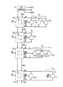
FIGURE 1 is a block schematic diagram of a digital circuit 10 comprised
of a plurality of individual circuit elements 12" 122, 123 ... 12m where m is an10 integer 2 two. The elements 121 - 12m are arranged in groups or stages 14~, 142,
143 ... 14n of two or more elements each where n is an integer < m. Each of the
elements 12l - 12m takes the form of a digital logic element, such as, for example, a
~AM, ROM, CAM, FIFO or Random Logic Element, which has a built-in, self-test
capability. In other words, each of the elements 12, - 12m is BIST'd. The number and
type of elements 12, - 12m present in the circuit 10 is dependent on its function, and it
should be understood that the circuit could include a larger or smaller number of
elements, arranged the same or differently from those shown in FIG. 1. Additionally,
the circuit 10 may also include other types of elements (not shown) which are not
BIST'd.
Generally, self-testing of each of the BIST'd elements 12, - 12m is carried
out by applying a start BIST signal, hereinafter referred to as an SBIST signal, to each
element. In response to the SBIST signal, each of the BIST'd elements 121 - 12m
executes a self-testing routine in accordance with its particular structure. The results of
the self-testing undertaken by each of the elements 12l - 12n, are reflected in the status
of a flag (not shown), referred to as a BIST flag, within each element. Typically, the
BIST flag within each of the elements 121 - 12m, which is usually one bit wide, is set to
zero for a "pass" condition (i.e., a successful self-test) while the flag is set to a binary
one for a "fail" condition (i.e., an unsuccessful test). The status of the BIST flag serves
as a "test signature" for that element. Once the BIST flag is set, each element generates
a BIST complete signal, hereinafter referred to as the BC signal, indicating that the
!. ,
~ - 20~2333
- 4 -
Even though the BIST'd elements 12 1 - 12m appear to have each
undergone successful self-testing, one or more elements may be defective because its
BIST flag is stuck at a binary ~ro (i.e., the BIST flag erroneously indicates a
successful test). To avoid a "false positive" test result, each of the elements
5 121 - 12m is supplied with a BIST flag check signal, referred to as a BFC signal, at
the completion of testing. The BFC signal serves to toggle the BIST flag within each
element. If the BIST flag toggles (i.e., changes state) in response to the BFC signal,
then the test result, reflected by the state of the BIST flag within the element, is
indeed accurate.
In accordance with the invention, control of the BIST function of the
BIST'd elements 12 1 -12m within the circuit 10 is accomplished by a BIST control
network 16. The network 16 is comprised of at least one, and preferably, a plurality
of, Standard BIST Resource Interface Controllers (SBRI(~s) 181,182,183...18 n,
each SBRIC controlling the BIST'd elements in a corresponding one of the stages
15 141 -14n~ respectively. As will be discussed in greater detail below with respect to
FIGS. 2 and 3, each of the SBRICs 181 - 18n typically comprises a five-state,
finite-state machine which initiates testing of those of the elements 181 - 18n in a
corresponding stage by broadcasting an SBIST signal to the elements in that stage.
Further, at the completion of testing, each of the SBRICs 181 - 18n broadcasts a20 BFC signal to the elements in its corresponding stage to toggle the BIST flag in each
element to check if the flag is stuck at a zero.
Each of the SBRICs 181 - 18n, in addition to supplying both the SBIST
and BFC signals, also serves to store the test ~ign~tllre of the elements in itscorresponding stage. The test signature is stored in each SBRIC within a User Data
25 Test Register (UTDR) 20, which, as will be described, typically takes the form of
one or more flip-flops. The UTDR 20 in each of the SBRICs 181 - 18 n is seriallycoupled with those of the other SBRICs in the network 16. In this way, the test
~ign~tl-res held by the SBRICs 181 - 18 n are concatenated and may be shifted out
from the network 16 by a technique such as boundary scan. For example, in the
30 network 16, the SBRICs 181 - 18n are coupled so that the UTDR 20 of the firstSBRIC 18 1 has its input coupled to a Test Data Output (TDO) of a boundary scan
test controller 21 and the last SBRIC 18 n has the output of its UTDR coupled to a
Test Data Input (TDI) of the controller. In this way, the concatçn~tç~l test signature
held by the SBRICs 181 ' 18 n can be shifted out to the boundary scan test controller
35 by shifting a string of kn bits through the network 16 of SBRICs, where k 2 1 and
corresponds to the number of flip-flops per SBRIC (not shown).
~ 2092333
s
As described earlier, each of the SBRICs 181 - 18 n, as generically
represented by the SBRIC 18 i where i=1,2,3...n, comprises a five-state, finite-state
machine, the state diagram of which is shown on FIG. 2. As depicted in FIG. 2, the
five states of the SBRIC 18 i comprise an IDLE state 22, a BIST execution state 24, a
5 FAIL state 26, a WAIT state 28, and a PASS state 30. At the outset of operation, the
SBRIC 18 i enters the IDLE state 22 of FIG. 2 during which time the SBRIC is
dormant. The SBRIC 18 i remains in the IDLE state 22 for as long as either of two
signals, Run BIST, hereinafter referred to as RB, and SBRIC 18 i - l complete,
hereinafter referred to as SBCi _ 1, is at a binary zero value. The signal RB is10 generated by the test controller 21 of FIG. 1 and is broadcast to the SBRIC 18 i. By
raising the logic state of the signal RB from a binary zero to a binary one, the test
controller 21 signals the SBRIC 18 i to initiate self-testing of the elements 12 1 - 12m
in its corresponding stage 14 i-
As will become better understood by FIG. 3, the signal SBCi _ 1, which
15 is generated by the SBRIC 18 i- 1, changes to a binary one level at the completion of
built-in self-testing of the elements in the stage 14i_l. By the same token, theSBRIC 18i will generate a binary one level signal SBCi when it has completed
built-in self-testing of the elements in its corresponding stage 14i. In this way, each
succeeding one of the SBRICs 18 1 - 18n in the network 16 of FIG. 1 is actuated in
20 sequence by the previous SBRIC to initiate self-testing Of its corresponding stage so
that the elements in the stages 141 -14n are self-tested in sequence.
When both the RB and SBC i -1 signals reach a binary one level, then
the SBRIC 18 i enters the BIST execution state 24 and generates a binary one level
SBIST signal which is broadcast to those of the elements 121 - 12m within the stage
25 14i. Normally, the SBRIC 18 i remains in the BIST execution state 24 until such
time as the elements within the stage 14i have each generated a binary one level BC
signal to in~licate that the element has completed self-testing. However, should any
of the elements in the stage 14i generate a binary one level BF' signal (i.e., a signal
obtained by logically OR'ing the individual BF signals) during the time the SBRIC
30 is in the BIST execution state 24, then the Fail state 26 is entered.
There is an important reason for entering the Fail state 26 immediately
upon receipt of a binary one level BF signal from any element in the stage 14i,
rather than waiting until the completion of testing of all of the elements in the stage.
In practice, the elements 121 - 12m are clocked at a much higher frequency than the
35 SBRICs 181 - 18m. Thus, an element within the stage 14i may complete its BISTroutine, then generate a binary one level BF to indicate a fault, and thereafter reset its
~ 2092333
- 6 -
BIST flag so as to now generate a binary zero BF signal, all well before the SBRIC
18 i has been notified that the other elements in the stage have each completed their
self-testing routines. Were the SBRIC 18 i to read the BIST flag of the element 12j
after it had been reset, the state of the BIST flag would reflect a pass condition when,
5 in fact, the element had actually failed.
The SBRIC 18 i enters the Wait state 28 from the BIST execution state
24 when each of the BC signals from the elements in the stage 14 i is at a binary one
level and each BF signal is at a binary zero level (i.e., BF' = 0). During the Wait
state 28, the SBRIC 18 i generates a binary one level BFC signal to toggle the BIST
10 flag elements within the corresponding stage 14i to check for a stuck-at-zerocondition. While in the Wait state 28, the SBRIC 18 i also generates a binary one
level SBCi signal to notify the next successive SBRIC 18i+l in the network 16 ofFM. 1 to initiate self-testing of the elements in its corresponding stage 14i+l.The SBRIC 18 i remains in its Wait state 28 for so long as the RB signal
15 supplied by the test controller 21 of FIG. 1 remains at a binary one level. In other
words, once the SBRIC 18 i has initi~ed built-in self-testing of the elements in its
corresponding stage 14 i and has actuated the next SBRIC 18 i + 1 in the network 16,
the SBRIC 18 i waits for the RB signal to become a binary zero, which occurs once
all of the SBRICs have been sequenced. The SBRIC 18 i leaves the Wait state 28
20 and either enters the Fail state 26, as mentioned earlier, or the Pass state 30,
depending on the status of each of the BF signals from the elements in the stage 14i.
If the RB signal is zero and one or more of the BF signals is at a binary
zero level, that is, BF' = O (infli~ting a stuck-at-zero condition of one or more of the
elem~nts in the stage), then the Fail state 26 is entered. Conversely, if the RB signal
25 is a binary zero, but all of the BF signals from the elements in the stage 14i are a
binary one (indicating a successful test and BIST flag check), then the Pass state 30
is entered. Once the SBRIC 18 i enters either the Fail state 26 or the Pass state 30,
the SBRIC remains in that state until a reset signal (from the test controller 21 of
FIG. 1) is asserted, or until the contents of the UTDR 20 are scanned out, and the
30 values corresponding to the Idle state 22 are scanned in. Thereafter, the SBRIC 18 i
returns to the Idle state 22. The Idle state 22 is also entered from the BIST execution
state 24 when RB goes to zero. Further, the Idle state 22 is entered from any other
state when a logic one-level RESET signal is applied.
Referring now to FIG. 3, there is shown a block schematic diagram of
35 the SBRIC 18 i (the SBRICs being identically configured to each other). The SBRIC
18i comprises three separate flip-flops 32, 34 and 36, respectively, which
2092333
_ 7
collectively comprise UTDR 20 of FIG. 2. Each of the flip-flops 32, 34, and 36 has
its input supplied with output of a separate one of a set of multiplexers 38, 40 and
42, respectively, each multiplexer being controlled by a signal SHIFTN generated by
the test controller 21 of FIG. 1. The first input of the multiplexer 38 is supplied with
5 a test signal from the TDO test controller 21 of FIG. 1 while the first input of each of
the multiplexers 40 and 42 is supplied with the output signal of a separate one of the
flip-flops 32 and 34, respectively. The output signal of the flip-flop 36 is coupled to
the TDI of the test controller 21.
The flip-flops 32, 34, and 36 each generate a separate one of a set of
10 output signals S0, Sl and S2, respectively, referred as state signals, which are
supplied to a combinational logic block 44. The logic block 44 is also supplied with
the RB signal from the test controller 21 of FIG. 1 and the signal SBC i - 1 from the
SBRIC 18 i - 1 (not shown). Additionally, the logic block 44 is supplied with the
output of an OR gate 46 and the output of each of a pair of AND gates 48 and 50.15 The OR and AND gates 46 and 48 serve to logically OR and AND the BF and BC
signals, respectively, generated by the elements (not shown) in the corresponding
stage 14 i (not shown) controlled by the SBRIC 18 i . The AND gate 50 serves to
logically AND all the BF signals to determine whether all the BIST flags change
state during the BIST flag check. For ease of reference the output signals of the OR
20 gate 46 and the AND gates 48 and 50 are designated by the terms BF', BC' and BF",
respectively.
The combinational logic block 44 is typically compri~e~l of a network of
individual gates (not shown) which is supplied at its inputs with the signals S0, S 1,
S2, RB, SBCi_l and the output signals of the gates 46, 48 and 50. In response to the
25 signaIs at its inputs, the combinational logic block 44 generates the signals SBIST
and BFC. Also, the block generates a set of signals NS0, NS 1, and NS2 which areeach supplied to the second input of a corresponding one of the multiplexers 32,34
and 36. During self-testing, the SHFTN signal is held at a binary zero so that the
multiplexers 32, 34 and 36 pass a separate one of the signals NS0, NS 1 and NS2 to a
30 respective one of the flip-flops 32, 34 and 36, respectively.
To better understand the relationship between the input signals supplied
to the combinational logic block 44, and the output signals generated thereby,
reference should be had to Table I below which contains two separate sets of entries
divided by a vertical double line.
,
~ 2092333
TABLE I
Current State RB SBCi_ 1 BF' BC' BF" Next State SBIST BFC SBci
Idle ~(l) O X X X X Idle 22 0 0 0
Idle ~(2) X O X X X Idle 22 0 0 0
Idle 22(3) 1 1 X X X sIsT Ex. 24 0 0 0
BIST Ex. 24(1) o X X X X Idle 22 o 0 0
BIST Ex. 24(2) 1 X X 0 X BIST Ex. 24 1 0 0
BIST Ex. 24(3) 1 X 0 1 X Wait 28 1 0 0
BIST Ex. 24(4) 1 X 1 X X Fail 26(1) 1 0 0
Wait 28(1) 1 X X X X Wait 28
Wait 28(2) o x x X 0 Fail 26(2)
Wait28(3) 0 X X X 1 Pass30
Fail 26(1) X X X X X Fail 26(4)
Pass 30(1) X X X X X Pass 30
The left-hand set of entries in Table I in~licfltes the relationship between each of the
five presently active states of the SBRIC 18i (Idle, BIST execution, Wait, Fail and
Pass) and the status of each of the input signals RB, SBCi _ 1. BF', BC' and BF" to
25 the logic block 44 during each state.
2092333
For each current state of the SBRIC 18 i, represented by an entry in the
left-hand side of Table I, there is a corresponding entr~v in the right-hand side of the
table. Each entr,v in the right-hand side of the table represents the next state of the
SBRIC that irnmediately follows the current state (the left-hand entry), and the state
5 of the output signals, BIST, BFC and SBCi for that next state.
As an example, at the outset of self-testing, the RB signal from the test
controller is a binary zero, so that the SBRIC 18 i is in the Idle state 22 (1), as
indicated by the first entry in the left-hand part of Table I. The status of the SBCi_ 1
signal, and the signals BF', BC' and BF", from the O~ gate 46 and the AND gates 48
10 and 50, respectively, are not of concern and therefore are depicted in the left-hand
portion of Table I as don't-care (x) values. From the Idle state 22 (1), the next state
of the SBRIC 18 i imm~i~tely following it is the Idle state 22 (1), at which time, the
signals SBIST, BFC and SBCi produced by the combinational logic block 44 are
each a binary zero. This state of affairs is consistent with that described in FIG. 2
15 since the SBRIC 18 i remains in the Idle state (22~ for as long as either of the RB and
SBCi_ 1 signals is a binary.
Now consider when the SBRIC 18i is cu~ ly in the BIST execution
state 24 (4) while the input signals RB and BF' are each a binary one and the BC,
SBCi and BF" signals are at don't-care values. From the BIST execution state 24
(4), the next state entered by the SBRIC 18 i is the Fail state 26 (1) at which time the
SBIST signal is at a binary one, while BFC and SBCi signals are each m~int~ined at
a binary zero. This state of affairs is consistent with that depicted in FIG. 2 since the
presence of a binar,v one level BF' signal indicates a failure in the testing of one or
more of the elements in the stage 14i.
At the completion of self-testing (i.e., while the SBRIC 18i of FIG. 3
remains in the Idle state 22 of FIG. 2), the SHFTN signal changes to a binary one
level. Once the SHFTN signal changes states, a stream of bits supplied at the TDI of
the SBRIC 18 i from the test controller 21 of FIG. 1 can be shifted through the flip-
flops 32, 34, and 36 of FIG. 3 to shift out the composite test signature of the
30 elements in the stage 14i which is held by these flip-flops.
When the RESET signal is asserted (RESET=l), the SBRIC 18 i will be
forced to enter the IDLE state 22 unconditionally.
The foregoing describes a network 16, comprised of one or more
standard BIST resource interface controllers 181 - 18 n for controlling the self-
35 testing of a plurality of BIST'd elements 12 1 - 12m.
'~- 2092333
- 10-
It is to be understood that the above-described embodiments are merely
illustrative of the principles of the invention. Various modifications and changes may
be made thereto by those skilled in the art which will embody the principles of the
invention and fall within the spirit and scope thereof.
For example, each SBRIC 18 i in the illustrated embodiment has been
configured to store a single composite test signature obtained by logically OR'ing
the test s;gn~tllres of the individual elements in the corresponding stage 14i. Rather
than store a composite test sign~t-lre, each SBRIC 18i could easily be modified to
store a multi-bit test signature, with each bit representing the individual test10 signature of a separate elçment in the stage.