Note: Descriptions are shown in the official language in which they were submitted.
300-923823-NA
SJ-91-24
ADAPTIVE SIGNAL MOI)Ur.ATION SYSTIEM
FIELD OF THE INVENTION:
This invention relates to digital signal modulation
that employs quadrature amplitude modulation and,
more particularly, to a digital signal modulator
that is adaptive in response to a command to alter
its modulated output.
BACKGROUND OF THE INVENTION
Quadrature amplitude modulation (QAM) of
transmission carriers by digital signals is a known
method of digital modulation. For two phase state
modulation, each bit has two reference phases, one
phase for a value corresponding to one and one
phase for a value corresponding to zero. The
phases are shifted by 180° from each other.
In a four-phase QAM (or quadrature-phase-shift-
keyer, QPSK) a carrier wave takes each of four
different phase values (90° separated depending on
the values assumed by two bits. Such a four phase
QAM (QPSK) is shown in Fig. 1 and includes a
quadrature phase shift keying (QPSK) circuit 10. A
pair of digital inputs D1 and D2 are applied to
mixers 12 and 14, respectively. The output of a
local oscillator 16 is applied to a 90° hybrid 18
where it is separated into sine and cosine values
that are respectively applied to mixers 12 and 14.
~~~L~~
2
The outputs from mixers 12 and 14 are summed in a
summing circuit 20 to provide an output on line 22.
While inputs D1 and D2 take the form of binary
values 1 and 0 within QPS~K 10, those values are
converted by level shifter's (not shown) to dl and
d2, which exhibit digital values of +1 and -1,
respectively. In this manner, a quadrature phase
output from summing circuit 20 appears in the form
of dla~~'ul.n~Jt + d2Aco~u'~'Jt a
In Fig. 2, the phases emanating from summing
circuit 20 are shown by an I/Q plot of phase
vectors 24, 26,, 28 and 30. If values d1 and d2 are
+1 and -1 respectively, the output signal on line
22 lags the phase of local oscillator 16 by 45°.
Similarly, if d1 and d2 are, respectively, -1 and
+1, the output phase lags by 135°, etc. QPSK 10 is
thus enabled to output four separate phase signals
in dependence upon the values of. inputs D1 and D2.
In Fig. 3, a QAM is shown that enables the
generation of 16 separate phase and amplitude
signals in accordance with four digital inputs Dl-
D4. In this instance, a pair of QPSK modulators 30
and 32 are employed, each operating identically to
QPSK 10 of Fig. 1. In this case, however, the
output of QPSK 32 is fed through a 6dB attenuator
34 before being applied to summing circuit 36. The
resulting output on line 38 is a vector addition of
the outputs of QPSK modulators 30 and 32 and is
shown in Fig. 4.
CA 02092452 2002-10-21
3
As an example, if the output from QPSK modulator 30
exhibits the phase shown by vector 40, and the output
from QPSK 32 is a signal having a phase as indicated by
vector 42, then the resulting signal on output line 38
exhibits a phase as shown by vector 43 to a point 44. The
16 states of the four digital inputs D1-D4 cause the
generation of a "constellation" of 16 points. A vector
drawn to each point illustrates the phase and amplitude
of a resultant output signal in response to the indicated
digital input values.
Various modifications of the above noted prior art
circuits appear in the following patents. In U.S. Patent
4,571,549 to Lods et al., a 16 QAM is shown that converts
a train of binary data signals into 16 predetermined
phase and amplitude values. In U.S. Patent 4,464,767 to
Bremer, multiple, synchronous, QAM transmitters are
employed that respond to an input binary bit pattern to
produce output signals having phase and amplitude states
defined by a 64 point constellation.
U.S. Patents 4,168,397 to Bradley and 4,804,931 to Hulick
show further versions of QAM devices for producing multi-
state outputs in accordance with digital signals. Bradley
describes an eight-phase PSK modulator, whereas Hulick
describes a multiphase quadrature system that employs a
plurality of cascaded combining circuits to achieve the
multiphase output. U.S. Patent 4,039,961 to Ishio
describes a demodulator for a 16 QAM signal wherein the
reference carrier is extracted from the
CA 02092452 2002-10-21
4
received signal and is regenerated for demodulation
purposes.
In all of the above noted prior art, the described
modulators provide regularly arrayed phase, amplitude
outputs in accordance with determined digital inputs. In
each instance, the phase output is predetermined by the
digital input value.
It is an object of an aspect of this invention to provide
a QAM system that is adaptive and can be adjusted in
accordance with transmission system element
characteristics.
It is another object of an aspect of this invention to
provide a digital modulation system that is adaptive and
enables adjustment of the converter's output in
accordance with predetermined control inputs.
It is a further object of an aspect of this invention to
provide a digital modulation system having a number of
output amplitude/phase states that greatly exceed the
number of possible digital transmission states, thereby
enabling amplitude/phase states to be selectively chosen
to compensate for non-linear and/or time dispersive
elements of a transmission system.
SUMMARY OF THE INVENTION
Digital signals are converted to phase and amplitude
altered, periodic, analog signals and emplaced on an
output link. The system is adaptive
CA 02092452 2002-10-21
5
and includes a plurality of simple quadrature phase shift
keying modulators, each modulator having a plurality of
controlling digital inputs, the state of which determines
which of a plurality of phase displaced signals will be
outputted. A ~ local oscillator provides a periodic
sinusoidal signal to each QPSK modulator. Summing
circuits combine the outputs of the modulators so as to
produce a constellation of phase and amplitude-displaced
output sinusoidal signals. A processor/mapper combination
enables conversion of a first set of digital inputs to a
different set of digital outputs in accordance with a
control input. Thus, the processor enables the alteration
of the constellation of outputs in accordance with a
control input, which may be indicative of the condition
of a transmission facility.
Accordingly, in one aspect of the present invention,
there is provided an adaptive system for converting input
digital signals to phase and amplitude adjusted periodic
signals for passage to a transmission means, said system
comprising:
a plurality of quadrature phase shift keying
modulators, each modulator connected to a common
oscillatory means and having a plurality of digital state
inputs, the states of said inputs determining which of a
plurality of quadrature phase displaced signals will be
outputted;
means for vectorially summing the outputs of said
modulators so as to enable production of a constellation
of phase and amplitude displaced outputs;
mapping means for matching a set of digital signal
inputs to a different set of digital states, said digital
states connected as controlling inputs to said quadrature
phase shift keying modulators, said mapping means storing
CA 02092452 2002-10-21
5a
a plurality of sets of digital states, said plurality
greater in number than that required to represent just
said digital signal inputs; and
processor means responsive to control inputs to
enable a said set of digital signal inputs to cause said
mapping means to output a set of digital states in
accordance with said control inputs, said input processor
means responsive to said control inputs to enable
selection of any of a plurality of sets of digital states
by said set of digital signal inputs, said vectorial
summing means producing phase and amplitude displaced
signals in accordance with said digital states.
In accordance with another aspect of the present
invention, there is provided a method for adaptively
converting digital signals to phase and amplitude shifted
carrier signals, said method comprising the steps of:
(a) converting a plurality of pairs of digital
signals to quadrature phase shifted carrier signals;
(b) attenuating one said quadrature phase shifted
carrier signal and vectorially summing it with a non-
attenuated quadrature phase shifted carrier signal;
(c) attenuating said vectorial sum from step (b)
and combining it with another said quadrature phase
shifted carrier signal;
(d) repeating steps (b) and (c) until a last summed
output appears at an output; and
(e) controlling states of said pairs of digital
signals in accordance with control signals and additional
digital inputs so as to enable a plurality of said
additional digital inputs to produce digital signals in
conformance with said control signals, there being more
values of said controlling states of said pairs of
digital signals than are required to represent said
CA 02092452 2002-10-21
5b
additional digital inputs.
DESCRIPTION OF THE DRAWINGS
An embodiment of the present invention will now be
described more fully with reference to the accompanying
drawings in which:
Fig. 1 is a block diagram of a prior art phase shift
keying modulator.
Fig. 2 is a vector diagram illustrating the four phase
vectors which result at the output from the circuit of
Fig. 1.
Fig. 3 is a block diagram of a 16 QAM circuit found in
the prior art.
Fig. 4 is a phase-vector plot illustrating the 16
constellation points that are produced by the operation
of the modulator of Fig. 3.
~~~~~W
6
Fig. 5 is a block diagram of a system for
converting digital signals to phase shifted
periodic analog signals, constructed in accordance
with the invention.
Fig. 6 is a plot of the canstellation of points in
phase space produced by the circuit of Fig. 5,
further illustrating 1~ points in the constellation
that are selected in accog~dance with 16 possible
states of a four bit control input.
Fig. 7 shows the circuit of Fig. 5 in combination
with a non-linear transmission element.
Figs. 8A-8E show representative phase/amplitude
constellations at various points in the circuit of
Fig. 7.
Figs. 9A and 9B show representative amplitude/phase
responses for a traveling wave tube amplifier, used
to obtain the constellations of Figs. 8A-8E.
Figs. 1~DA and 10B sh~w representative AM/QM and
AM/AM distortions for a traveling wave amplifier,
used to obtain the constellations of Figs. 8A-8E.
DETAILED DESCRIPTION OF THE TNVENTION
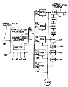
The modulator shown in Fig. 5 builds up~n the prior
art modulator shown in Fig. 3. The number of ~PSK
modulators that comprise the circuit of Fig. 5 are
determined by the precision required of the output
constellation. For purposes of explanation, five
QPSK modulators are shown which enable a potential
constellation of 1024 possible phase-amplitude
states (2'~) . Each QPSK modulator is controlled by
two binary inputs, with a ten bit binary word Dl-
D10 controlling the entire modulator.
Each QPSK modulator is capable of outputting a
local oscillator signal with one of 4 phase states.
Thus, QPSK madulator 100, in accordance with the
states of bits D9 and D10, will produce one of 4
phase outputs. In a similar manner, QPSK modulator
102 wall produce (in dependence upon the states of
bits D7 and D8) a local oscillator frequency signal
having one of 4 phase states. The output of QPSK
modulator 100 is passed through a 6d8 attenuator
and is summed (vectorially) in summing circuit 106
with the output from QPSK modulator 102. The
result is passed through 6 dB attenuator 108 to
summing circuit 110 and the procedure is repeated
until the last of the summing circuits is reached
(i.e., summing circuit 112). The resulting output
on line 114 includes a signal having a phase-
amplitude state constellation that results from a
combination of the summed outputs of all the QPSK
modulators, in accordance with the states of data
input bits D1-D10.
Four binary inputs A1-Fr4 are applied to a
constellation processor 130. It is to be
understood that binary inputs A1-A4 are selected
merely for explanation purposes and other numbers
of binary inputs may be used to control the
operation of the circuit of Fig. ~. A
2~~~~~~
constellation control input 134 is applied to
constellation processor 130 and controls which of
1024 possible bit states of digital outputs D1-D10
are addressed in a mappex 132 by various states of
inputs A1-A4.
As is known, binary valuea on inputs A1-A4 can
exhibit any one of 16 separate digital bit
patterns. Each bit pattern causes constellation
processor 130 to address a particular set of bits
D1-D10 in mapper 132 (in accordance with a command
on input 134). The selected states of bits D1-D10
control the operation of 'the QPSK modulators to
provide a particular phase amplitude signal state
on output line 11~. Thus, the 16 states that can
appear on input lines A1-A4 cause 16 (of a possible
1024) separate bit states on output lines D1-D10.
In Fig. 6, a plot shows the 32 ~ 32 constellation
of phase amplitude vector points that can be
generated by the circuit of Fig. 5. Each vector
originates at the intersection of the I/~ axes and
proceeds to an intersection of the grid plotted on
the graph. 16 separate points in the constellation
are illustrated to enable visualization of the
analog phase values that are created (in this
example) from digital inputs A1-A4. By altering
the commands on constellation control input 134,
processor 130 can be caused to change the matching
of the states on inputs A1-A4 to the states of D1-
D10 in mapper 132. Thus, in the event of non-
linear distortion on output line 114 (or a
transmission element connected thereto), the analog
~~~~~~~5',
9
outputs thereon (corresponding to inputs A1-A4) may
be rearranged so that they compensate for the
expected distortions. Such ''rearrangement°' is
accomplished by a constellation adjuster function
135 in constellation proces:5or 130. The operation
of adjuster function 135 wi:l1 be further explained
fn the discussion of Fig. 7.
7Cn summary, the c;uadrature phase shift keyers shown
in Fig. 5 are capable of providing analog outputs
with any of 1024 phase relationships. Those
phase/amplitude relationships are controlled by
digital values appearing on inputs D1-D10. The
specific binary values emplaced on inputs D1-D10
are controlled by constellation processor 130 in
accordance with a constellation control input 134
and the contents of mapper 132. Thus, the 16
states of inputs A1-A4 can be matched to any of 16
of the 1024 values of D1-D10 and cause
corresponding analogue phase outputs to be placed
on line 114.
In Fig. 7, the system of Fig. 5 is shown employed
in combination with a non-linear transmission
element, in this case, a schematically shown
traveling wave tube amplifier (TWTA) 200. TWTA 200
can be modeled as a bandpass filter (BPFj 202
followed by a non-linear element (NLE) 204. The
system's objective is to suppress intersymbol
interference at the input to NhE 204, since once
NLE 204 acts upon a signal corrupted by significant
intersymbol interference, the resulting performance
degradation (bit error rate vs. signal-to-noise
~~~~9~~a~'
ratio) is largely unrecoverable.
Within constellation proce:~sor 130 is shown three
functions that enable the generation of a properly
oriented constellation to overcome transmission
non-linearities of TWTA ;200. Mapper 132, as
aforedescribed, provides an initial mapping of
inputs A1-A4 to a vector defined by one
constellation point in a regular 16 QAM
constellation (for example), such as shown in Fig.
8A. The resulting digital phase and amplitude of
the chosen vector is fed to a constellation
adjuster function 135 that includes a non-linear
compensation function 210 and a transversal
equalizer 212. Non-linear compensation function
has been pre-loaded to enable it to adjust the
output from mapper 132 to compensate for the non-
linearities to be experienced in NLB 204 (such as
AM/AM and AM/PM distortion). More specifically,
non-linear compensation function 210 modifies the
phase and amplitude of the phase vector from mapper
132 so as to complement the expected effects of NLB
204. A representative altered constellation output
from non-linear compensation function 210 is shown
at Fig. 8B.
The output from non-linear compensation function
210 is fed to a transversal equalizer 212 (e.g., a
finite impulse response filter) to enable the
inputs to NLB 204 to have minimal intersymbol
interference. Coefficients and delays within
transversal equalizer 212 are selected and pre-
loaded in accordance with the transmitted symbol
11
rate and impulse response of BPF 202. In this
manner, symbols inputted to BILE 204 have minimum
TST at the ideal sampling instant of the waveform.
Transversal equalizer 27.2 is only required in cases
where the principal spectrum of the output is
comparable to the bandwidth of BPF 202, and cases
where the impulse response of BPF 202 is comparable
to the time duration of a transmission symbol. The
response of the system from the input of
transversal equalizer 212 to the output of BPF 202
is thus essentially free of inter symbol
interference. A representative canstellation output
from transversal equalizer 212 is shown at Fig. 8C.
Those skilled in the art will realize that the
functions of mapper 7.32 and non°linear compensator
210 may be combined into a single function since
the mapping function can map its inputs onto a
predistorted map. This mapping function can be
implemented as a RAPZ look-up table. Thus, in
situations where the characteristics of NLE 204 are
subject to drift due to component ageing or other
causes, the table can be adapted accordingly.
Figures 8A-8E show constellations corresponding to
points A-E of figure 7. An example constellation,
i.e, a 1~ SAM, is given in Fig. 8A. After the
action of non-linear compensator 210, the
constellation of Fig. 8B results and no longer
resembles a conventional 16 QAM. The transversal
equalization injects intersymbol interference and
the constellation of Fig. 8C is the result. After
~~~~3~!~Rr
12
passing through the bandshape distortion of BPF
200, constellation D results (Fig. 8D). Note that
most of the ISI is removed.
Finally the TWTA non-linear distortions in NbE 209
reverse the previously forced constellation
distortions and a famil3aa:~ 7.6 SAM constellation
appears (Fig. 8~). Some residual constellation
spreading is apparent, particularly in the inner
states attributable to imperfect transversal
equalization compensation of BPF 202. This results
from non-linear distortion operating on the non-
fully equalized constellation at D, coupled with
the higher gain for the inner states (small signals
in the TWTA) compared with a lower gain for the
outer states (nearing TWTA saturation).
It must be recognized that point D does not
physically exist, but is a conceptual interface in
the hypothetical TWTA model. The non-linearities
and bandshaping of TWTA 200 that were used in
deriving the constellations of Figs. 8A-8~ are
shown in Figs. 9A, 9B, 10A and 30~.
It should be understood that the foregoing
description is only illustrative of the invention.
various alternatives and modifications can be
devised by those skilled in the art without
departing from the invention. For instance,
compensation for time dispersive elements in the
transmission medium (filters, propagation media)
may be per. formed by combining successive data words
(Al-A4) with appropriate digitally controlled
~~9~I~.~~a
3. 3
combining coefficients to create "conjugate"
intersymbol interference. This interference and
the resulting signal at the medium output has far
less intersymbol interference. The result is that
the signal thus processed, exhibits a lower overall
probability of bit error in the presence of medium
induced noise than if this "conjugate°' intersymbol
interference was not included. Accordingly, the
present invention is intended to embrace all such
alternatives, modifications and variances which
fall within the scope of the appended claims.