Note: Descriptions are shown in the official language in which they were submitted.
f ~
SE~ICONDUCTOR DEVICE
This invention relates to a semiconductor device
carrying a semiconductor device chip operating a high speed
~or use in a microprocessor, a memory device, etc~
Today's semiconductor device chips used mainly in
microprocessors have increased numbers of signal inputs and
outputs and operate at high speed~ This has caused the
probLem of noises such as switching noises produced during
switching o~ the device chips, re~lection noises produced
at the wiring ends and cross-talks produced between
wirings~ Further since the electric power consumed by
these device chips are rather Large, it is becoming an
important probLem how the heat produced in the
semiconductor device should be reLeased.
Heretofore, it was an ordinary practice to mount
passive devices such as capacitors and resistors on the
printed wiring board carrying a semiconductor device chip
in order to reduce the above-mentioned noises. ~ut ~his
method has a probLem in that t~e wiring inductance tends to
be large because of a long distance between the
semiconductor device chip and the passive devices on the
printed ~iring board~ Further 7 since the passive devîces
take up ~ subs~antial space on the printed wiring board7 it
is difficult to reduce noise or increase the mounting
~7~ ~ 3
density beyond a certain limit~
On the other hand, in order to reduce noise most
effectively, noise reduction should be provided as close as
possible to the semiconductor device chip~ With this
arrangement, the wiring lengths can be shortened. Thus, a
conventionaL ceramic laminated package has internal wirings
in a muLti-layered structure in order to reduce the power
source inductance, has capacitors between internal wirings
in order to bypass noise, and has internal power~ground
plane means for reducing crosstalks~
Further, in order to improve the heat radiating
capacity, some of conventional laminated ceramic packages
are made of alumina and are provided with a heat sink made
of Cu-W alloy, or made of material aluminum nitride, which
is known to ha~e a higher thermal conductivity than
alumina. Also~, there are known packages provided with heat
radiating fins.
Such con~entional ceramic laminated packages comprise
a body formed by laminating a ceramic sheet suitable for
formation of circuits and the mounting of high-speed device
chips and a high-melting point metal sheet and baking them
together, and a semiconductor mounted thereon. After
connecting the semiconductor device chip to necessary
parts, the package body is sealed by a cap formed of a
metal plate or ceramic plate and lead pins are bonded to
the outer side of the package~ Such packages are difficult
to mass-produce even if the manufacturing steps are
automated~ Thus, their production cost is rather high~
Those having mea~s for improving heat radiating capacity
are especially expensive~
Al~o, it is rather difficult ~o adapt such a
conventional ceramic laminated package to various purposes~
For e~ample, if it is desired to change the type of the
package or the built-in circuit according to change in the
i~tended use, it will be necessary to redesign the entire
package~
In contrast, plastic package type semiconductor
devices are more adapted for mass-production and can be
formed by transfer molding at low cost~ Further, the lead
frame can be secured in position more reliably.
But this type of devices ordinarily use only a lead
frame, so that it is impossible to prevent internal noise~
Especially if a high-speed device chip is mounted on such a
device, it is difficult to reduce noises to a satisfactory
level~
One possible way to improve the heat radiating
capacity of a plastic package is to provide a heat spreader
made of copper alloy~ In case of a ceramic package, heat
sinks and heat radiating fins are used~ But semicon~uc~or
devices equipped with such heat radiating means are large
in volume. heavy in weight and expensive. Such packages
are not suitable for use in general-purpose semiconductor
devices.
Thus, there was no conventional package which
satisfies aLl of the folLowing four conditions: 1)
inexpensive, 2) having such high anti-noise properties as
to be adaptable to high-speed operation, 3) flexible to
cope with a wide variety of applications, and 4) high in
heat radiating capacity.
It is an object of this invention to provide a
semiconductor device which has a board for mounting a
semiconductor device chip, a lead frame and a laminated
ceramic plate and which satisfies the abovesaid conditions
1~ - 3) or 1) - 4) in a balanced manner.
From one aspect of the present invention, there is
provided a semiconductor device comprising a metal board, a
semiconductor device chip mounted on the metal board, a
ceramic laminated wiring board having wiring layers and
mounted on the metal board so as to surround the
semiconductor device chip, and a lead frame bonded to the
ceramic laminated wiring board throu~h an insulating layer,
the semiconductor device chip. the ceramic laminated wiring
board and the lead frame having their inner portions sealed
with a synthetic resin. (This structure is hereinafter
referred to as the first arrangement.)
~S ~ t~ f'J
From anoth~r aspect of the present invention, there is
provided a semicqnduc~cr device which is similar to the
device ot` the first arrangement e~cept that the ceramic
laminated wiring ooard has a device chip mounting por~ion
and is provided with a wiring Layer on its surface and/or
between its layers and,~or on its back~ (This structure is
hereinafter referred to as the second arrangement~) This
means that in the second arrangement, the metal board used
in the first arrangement is replaced with a single layer or
multi-layered ceramic pLate~
The ceramic laminated wiring board used in the first
or second arrangement should be mainly made of aluminum
nitride rather than alumina in order to insure high heat
radiation~
If the wiring board is mainly made of aluminum
nitride, at least the outer ends of the wiring layer
provided on the surface of the wiring board may have the
same shape as the inner ends of the corresponding leads of
the lead frame, the leads being directly bonded to the
wiring layer by soldering or hot-pressing~ (This structure
is referred to as the third arrangement.)
In the first and second arrangement~, via holes filled
with a conductiv~ material may be formed in the insulating
layer at portions right under ~he leads, thereby
electrically connecting the lead frame ~o the wiring board
,~ ~
7 ~
through the conductlve material in ~he via holes. Such
via-connection may be used in combination with other
connecting methods which will be shot~n in the description
of embodiments.
Ln the first and second arrangements. a wiring layer
may be provided on the surface of the wiring board to cover
only its intermediate portion around the device chip
mounting portion or to cover only its outermost portion
disposed around the intermediate portion. Otherwise~ two
separate wiring layers may be provided on the surface of
the wiring board~ one on the outermost portion and the
other on the intermediate portion. In any of the above
three cases, the lead frame is provided on the insulating
adhesive layer so as to be disposed over the outermost
portion of the wiring board~ The wiring layer provided on
the intermediate portion of the wiring board serves as a
relay connecting the semiconductor device electrode to the
lead frame~ The wiring layer on the outermost portion is
used as a circuit exclusively for power source or
grounding.
The lead frame is preferably made of copper alloy if
high heat radiation is required~ The wiring layers of the
wiring board may be electrically connected together through
via-connection or crossover connection which will be
described hereinbelow.
Further, the wiring layers of the wiring board may
include a layer exclusively for grounding or power source
potential or a layer having passive devices such as
resistors~ Also~ in order to improve the anti-noise
properties, a bypass capacitor may be formed in the wiring
board, utilizing two of the wiring layers as its electrodes
and one of the insuLating layers as its dielectric.
In order to further reduce the size of the device, the
wiring layer provided on the surface of the wiring board
may be formed by the film process or the above-mentioned
passive devices may be film devices~
The semiconductor device according to the present
invention is advantageous over the conventional
semiconductor device which uses a laminated ceramic board
itself as a sealing package, such as a pin grid array tPGA),
in that an expensive laminated ceramic portion can be made
compact in size. Such downsizing of the ceramic portion is
possible because ceramics are not used for sealing the
device, wire connections are made on the surface of the
board, so that no e~tra internal wirings are necessary~ and
wiring layers can be formed not only on the surface of the
laminated ceramic board but on other surfaces. Further,
since the entire devics can be resin-sealed by transfer
molding, its mass-productivity is high. Thus, the
semiconductor device of the present invention even with the
lead frame is more inexpensive than conventional CPGA's~
By using laminated ceramic board, it is possible to
form in the internal wiring a bypass capacitor having
electrodes formed by some of the internal wirings or to
form damping resistors or terminal resistors in the surface
wiring. It is also possibLe to reduce the inductance of
the power source circuit by providing a plurality o~ wiring
layers or by using some of the wiring layers e~clusi~ely
for power source or grounding. Thus, the device of the
present inventian has excellent anti-noise properties
comparable to those of CPGA's~ By employing a circuit
arrangement in which an insulating layer between the leads
and a wiring layer functions as a dielectric or a circuit
arrangement in which the leads have a microstrip structure
by use of the metallized layer formed on the surface, the
anti-noise prdperties will improve even higher than those
of CP~A's.
Further t the ceramic laminated wiring board and ~he
lead frame can be replaced with different types and~the way
of wiring connections can be changed. In other words, the
de~ice can be redesigned easily according to the intended
use and thus can be used for various purposes.
It is possible to improve the heat radiating capacity
by properly selecting the main component of the materials
forming the ceramic laminated wiring board and the lead
frame~ For example, by forming the ceramic board from
aluminum nitride, which is high in heat radiating capacity
and forming the lead fra~e and the metal board from copper
alloy, which is high in heat conductivity, the entire
device will s~low such a high heat radiating capacity that
it is possible to mount a device chip having a high heat
val.ue~
The semiconductor device of the present invention
comprises a ceramic laminated wiring board and a lead
frame. After mounting a semiconductor device chip and
connecting it to necessary parts, the device is resin-
sealed by trans~er molding. Thus, its mass-productivity is
high~
It is possible to increase the anti-noise properties
by providing bypass capacitors or a layer used exclusively ~.
for the power source or grounding in the wiring board, by
providing passive devices in the surface wirings, or by
connecting the leads to the wirings through via-connection~
Thus, it can be used for high-speed operation~
Further7 this device can be used for various purposes,
because it is possible to change selectively the internal
structure of the ceramic laminated wiring board, the number
of its layers, its ceramic material, the wiring pattern on
the wirin~ board, the capacity and the mounting position of
the device chip mounted on the board, the electrostatic
capacity of the bypass capacitors, the materiaL of the lead
frame, and the way of connections between parts~
High heat radiating capacity can be achieved by
combining a wiring board made mainly of ALN and a lead
~rame made of copper aLloy. The semiconductor device of
this invention is especially suited for use as a substitute
for a conventional semiconductor device which necessarily
required an expensive ceramic laminated pac~age~ such as a
semiconductor device carrying a high-speed digital IC,
typically an MPU, or a semiconductor device carrying a
memory device required to input and output signals at high
speed. The semiconductor device according to the present
invention is versatile, less expensive and of high
performance~
Other ~eatures and objects of the present invention
will become apparent from the following description made
with reference ~o the accompan~ing drawings, in which:
Fig. 1 is an e~ploded perspective view of a
semiconductor device of the first arrangement;
Fig~ 2 is a sectional view of an embodimen~ of a
semiconductor device of the first arrangement before
resin-~ealed;
Fig. 3 is a sectional view of another embodiment of a
semiconductor device of the first arrangement before
resin-sealed;
it )
Fig~ 4 is a sectional view of still another embodiment
of semiconductor device of the first arrangement before
resin-sealed;
Fig. S is an exploded perspective view of a
semiconductor device of the second arrangement;
Fig~ 6 is a schematic plan view of an example of
wirings provided on the surface of the wiring board;
Fig. 7 is a schematic plan view of another example of
surface wirings;
Fig. 8 is a schematic plan view of a still another
example of surface wirings;
Fig~ 9 is a schematic plan view of surface wirings
made of films and including film resistors;
Fig. lO is a schematic sectional view of a ceramic
laminated board used in a semiconductor device of the
second arrangement;
Fig. Il is a schematic sectional view of a board
formed inside with a bypass capacitor;
Fig. 12 is a plan view of the lowermost wiring for
power source potential shown in Fig. 10, which is connected
at four points through via-connection;
Fig. 13 is a sectional view of a laminated ceramic
wiring board used in an experiment;
FiV . 14 is an e~ploded perspective view of a
semiconductor device of the third arrangement;
~ i 1 J ~ 7 ~ ,~
Fig. 15 is a schematic plan vie~ of an example of
wirings provided on the surface of the wiring board shown
in Fig~ 14;
Fig~ 16 is a sectional view of a laminated ceramic
wiring board used in an experiment;
Fig. 17 is a sectional view of another embodiment of
ceramic laminated wiring board for use in a semiconductor
device of the second arrangement;
Fig~ 18 is a sectional view of the wirings on the
board of Fig~ 17 showing how they are connected together;
Fig~ 19 is a plan view showing an example of crossover
connections between the wirings of the board shown in Fig.
17;
Fig~ 20 is a plan view of the crossover connections of
Fig~ 17 in a completed form; and
Fig~ 21 is a sectional view taken along line X-X of
Fig~ 20~
The emoodiments of this invention will be described in
detail with reference to the drawings~
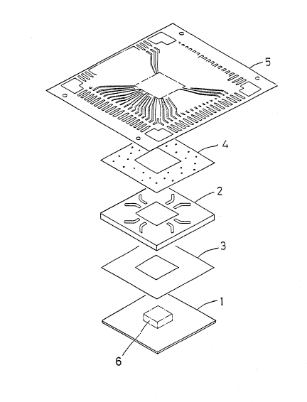
Fig~ 1 is an exploded schematic view of the
semiconductor device in the first arrangement~ In this
embodiment, the device comprises, from under to top, a
metal board 1 in the center of which a semiconductor device
chip B is to be mounted, an insulating layer 2 made of an
insulating adhesive or an insuiating double-sided adhesive
h ~
tape, a ceramic laminated wiring board 3, an organic film 4
(such as a polyimide fiLm) having an insulating adhesive
applied to both sides thereof, and a
lead frame S made of copper alloy or ironJnickel alloy~
Thou6h not shown, electrical connections are provided
between the semiconductor device chip ~ and the ceramic
laminated wiring board 3 and between the latter and the
lead frame 5~ The lead frame 6 is then resin-sealed by
transfer molding over the entire area except its outer
portion and finally the leads are separated from one
another by cutting off the outer edge portion of the lead
frame 5~
As a semiconductor de~ice having such a basic
structure, we made a plastic quad flat package tPQFP~
carrying a CMOS digital logic IC device~ The package is 24
x 24 ~ 4 ~mm) in dimension and has 33 leadæ on each side
which are arranged a~ the pitch of 0.64 mm~
Fig~ Z shows a section of one of the semiconductor
device made~ The ceramic laminated wiring board 3 shown in
this figure is formed by laminating and baking alumina and
has a pair of comb-shaPed elec~rodes 7 and 8 made of
tungsten between the adiacent alumina layers. These
electrodes 7 and 8 are formed by printing on the respective
alumina layers and baking them together with the alumina
layers~ Inside the board 3, a capacitor is formed by the
~f~327~ l
electrodes 7 and 8 and the alumina layer disposed between
the electrodes as a dielectric.
The electrodes 7 and 8 are connected, respectively, to
wirings 9, 10, 11 and 12 formed on the surface of the
ceramic laminated wiring board 3~ These wirings are plated
with Au~
The eLectrode 7 is connected to a lead 5a through a
wire Wl branching from the wiring 9~ The wire Wl is taken
from the wiring ~ by wire bonding and extends through a
cutout 15 formed în the organic film 4. The electrode 7 is
connected to a tqrminal of the semiconductor device chip 6
through a wire W2 taken from the wiring 10 by wire bonding~
Thus, the lead Sa is electrically connected to the terminal
of the semiconductor device chip 6 via wire Wl, electrode 7
and wire ~2.
Similarly; the electrode 8 is connected to another
lead (not shown) through a wire W3 and to the terminal of
the semiconductor device chip 6 through a wire W4~ Thus,
assuming that the lead 5a has a power supply potential and
the other lead connected to the electrode 8 has a ground
potential, a noise-bypassing capacitor is provided paraLlel
to the p~wer supply, its electrodes being the electrodes 7
and 8. This c~pacitor absorbs the switching noise of the
semiconductor device chip 6.
Between a pair of film wirings 13 and 14 formed on the
L4
surface of the ceramic laminated wiring board 3, a resistor
18 made of ruthenium oxide and formed by thick-film
printing is inserted~
Wiring 13 is connected to a lead 5b through a
conductive material 17 filling a via hole 1~ formed through
the organic film 4 (or through the film 4 and the lead)~
The conductive material may be an epoxy resin containing an
Ag filler~ The other wiring 14 is connected to a terminal
of the semiconductor device chip 6 through a wire W5
connected by bonding~ Thus, by using the lead 5b, which is
connected to the terminal of the semiconductor device chip
6 through the conductive material 17, resistor 18 and ~ire
W5, to transmit high-speed signals, the resistor 18 will
serve to control the waveforms of the high-speed signals,
thus reducing the signal noises~
Fig~ 3 shows a section o~ a second embodiment. In
this figure, the same elements as those in Fig~ 2 are
denoted by like numerals and their description is omitted~
We will describe only the differences from the arrangement
shown in Fig. 2~
The semiconductor device shown in Fig. 3 is different
from the device shown in Fig. 2 in that the ceramic
laminated wiring board 3 is formed by laminating and baking
aluminium nitride (AlN), that after appl~ing a polyimide
film 1~ on the surface of the board 3, the wirings are
~, ~ t ~ ~ ~ ~
formed thereon, and that a resistor 20 provided on the
board 3 is formed of a film.
The surface of the ceramic laminated wiring board 3 is
mirror-finished, on which is provided the poLyimide film 19
by spîn-coating and baking~ Then, a TaN film as the
resistor 20 is formed by sputtering~ Film wirings are
laminated further thereon to form the wirings~ The film
wirings are formed by laminating Cr film for bonding and Cu
films shaped into a predetermined wiring pattern by vacuum
deposition and providing further thereon a protective layer
in the form of a chemically stable Au plating layer.
The polyimide film 19, the TaN film resistor 20 and
the film ~irings having a three-layer structure comprising
a Cr film, a Cu film and an Au plating may be formed by
photolithography in which uni~ormly shaped films are
subjected to etching to form a predetermined pattern or by
masking in which~ when forming the respective films, they
are individually subiected to masking to form the
respective patterns one after another~
Since this semiconductor device has the noise-
bypassing capacitor and the resistor 20~ noise can be
reduced ~s effectively as with the device shown in Fig~ Z.
Also, since the board is formed of aLuminum nitride and
the wirings and the passive device (resistor 20) provided
on the surface of board are in the form of films~ the
16
device of this embodiment is improved in heat dissipating
properties and compactness over the device of Fig. 2.
The polyimide film L9 can be alternatively an SiOxNy
insulating ~ilm formed by the C~D method~ The wirings
~ormed on this fiLm may have a multi-layered structure
comprising alternately laminated film wirings and
insulating films.
Fig~ 4 shows section of a third embodiment.
This device has a resistor 21, which is a chip part,
mounted on a ceramic laminated wiring board 3 made mainly
of alumina and~or AlN~ The resistor 21 has both ends
thereof soldered to wirings 22 and 23 on the board 3. On
the other hand, the wiring 23 is com1ected to a terminal of
the semiconductor device chip 6 through wire W5 and the
wiring 22 is conn~cted to the lead 5b through the
conductive material 17 in the via hole. Thus, the resistor
21 is formed between the lead 5b and the semiconductor
device chip 6. rt serves to control the waveform of the
aforementioned high-speed signals.
We manufactured PQFP samples having the above-
described structure. In any sample, the bypa~s capacitors
and resistors operated efficiently. ~ven when the number
of switching operations was increased, the input~output
signals showed no problematic waveforms. In case of
conventional plastic packages (PQFP's having the same outer
~ J~
dimensions as the above samples3 having a similar digital
logic IC mounted thereon, the input/output signals showed
noise ~aveforms~
The passive device mounted on the board 3 is not
limited to a resistor. For example, a capacitor, which is
a chip part, may be connected in parallel to the power
supply of the semiconductor device chip 6 by forming a
predetermined wiring pattern on the board 3~ The capacitor
can absorb switching noises of the semiconductor devi~e
chip 6. rn this case, there is no need to provide a
separate capacitor in the wiring board 3~ Thus, the wiring
board 3 may be a single-layer board having no capacitor
inside~ Also, the internal wiring layers may be used
e~clusively for the power supply or for grounding.
In the above embodiments, instead of connecting the
wirings on the ceramic laminated wiring board 3 to the
leads through bonding wires, they may be connected through
bonding tapes by auto-bonding through the cutouts 15.
Otherwise, the leads may be directly connected at the
cutouts 15 to the wirings on the board by hot-pressing or
soldering. Also, they may be connected through an
anisotropic conductive rPsin filling the cutouts 15.
On the other hand, among the leads of the lead frame,
ones connected not through the wiring board but direc~ly to
terminals of the semiconductor device chip may be connected
18
, .
by use of bonding ~ires or bonding tapes.
The via-connection which utilizes the conductive
material in the via holes 16 makes it possi~le to minimi2e
the length Or connection bet~een the leads and the
respective ~irings on t~e ~iri~g board and thus to further
lower the noise and the inductance of the signal
transmission paths. Also, this arrangement eliminates the
necessity of providing a space for connection between the
~irings and the leads~ Thus, the size of the entire device
can be reduced~ Further, it is possible to adjust the
impedance among the leads and the wirings by changing the
positions at which the via holes are formed~ For the above
reasons, the signal transmission leads are preferably
connected ~y via-connection though any of the
a~ovementioned connecting structures may be employed~
Fig~ 5 shows the basic structure of a ~iring board for
use in a semiconductor device in the second arrangement~
A ceramic laminated wiring board 31 is provided at the
central part with a device chip mounting portion 32 (which
may be a cavity)~ A peripheral area 33 surrounds the
device chip mounting portion 32~ Surface wirings 34 are
provided in the area 33~
The insulating organic film 4 such as a polyimide film
has an insulating adhesive appLied to both surfaces
t~ereof~ This organic film 4 is bonded to the peripheral
19
,
r~
area 33 and then the inner portion of the lead frame 5 is
bonded to the film 4 to form a wiring board having leads.
The semiconductor device chip 6 is mounted on the wiring
board 31 thus ~ormed~ After connecting necessary parts
together, the entire part of the lead frame 5 other than
its outer portion is resin-sealed~ Finally, the peripheral
portion of the lead ~rame is cut off to form the intended
semiconductor device~
The organic film 4 may be omitted if a ceramic film is
provided on the outermost layer of the wiring board 31 (in
which case, the wirings 34 are not sur~ace wirings any
more)~
Thus, the wiring board used in the second arrangement
may be made of ceramic including the portion which is made
of metal in the first arrangement~ Also, the position and
pattern of the wiring layers to be provided on the surface
of the wiring board are not limited~
For example, in the ~xample shown in Fig~ 6, wirings
34a to be connected to the semiconductor device chip 6
through bonding wires W are provided on the inner portion
of the peripheral area 33 and wirings 34b having at least
their outer ends shaped so as to correspond to the inner
portions of the respective leads are provided on the outer
portion of the peripheral area.
The lead frame 5 is bonded so that its leads overlie
the corresponding wirings 34b through the organic film 4
shown in Fig. 5 and are electrically connected thereto by
means of the via-connection as shown in Fig~ 2~ At least
some of the wirings 34a and 34b are electrically connected
together through an internal wiring 35 in the wiring board
31 as shown in Fig~ 10~
This arran~ement makes it possible to reduce the
number of bonding wires for connecting the leads directly
to the semiconductor device chip to zero or considerably
and thus to simplify the wiring and reducing the inductance
of the supply line~ Also, this makes it possible to form a
bypass power capacitor as described above in the wiring
board by using a plurality of layers of the internal
wirings~
Fig~ 7 shows an embodiment in which only relay wirings
34a are provided on the surface of the ceramic laminated
wiring board 31~ Namely, no wirings 34b as shown in Fig~ 6
are provided~ In this case, the lead frame is bonded to
the outer portion of the peripheral area 33 where there are
no surface wirings. The laads are electrically connected
to the wirings 34a through bonding wires or bonding tapes.
Some of the wirings 34a are connected to thP internal
wirings in the board through via-connection.
In the embodiment shown in Fig. 8, a wiring 34c
is provided on the outer portion of the peripheral area 33
~ ~3 ~ ~ r ~ ! 1,7
The lead frame is bonded to the outer portion through an
organic film having an adhesive applied to both sides. The
grounding or power supply lead is connected to the wiring
34c through ~ia-connection, while necessary ones of the
remainin~ leads are connected to the semiconductor device
chip via wirings 34a by bonding wires.
The wiring 34c may have the shape of a picture frame
as shown or may comprise a plurality of separate parts. In
the latter case, parts having a grounding potential and
parts having a power supply potential may be arranged
alternately with each other. In this arrangement, the
leads are overlaid on the parts of the wiring 34c having a
power supply potential and parts having a grounding
potential through the insulating layer. In other words,
the leads thus formed have a micro-strip structure. Thus,
the noise in the leads can be reduced though depending on
the electrostatic capacity of the interposed insulating
layer.
In the embodiment of Fig. ~, the wiring 34c has a
grounding potential, i.e. a grounding wiring 34a is
connected to the wiring 34c. But the wiring 34c may be
isolated from any other wirings.
In the second arrangement, too, the leads are
preferably connected to corresponding wirings through via-
connection for the aforementioned reason. But other
22
7 i~ ~
connections may be employed together with via-connection.
If high heat radiation is desired, the wirin~ board
may be made of AlN having a high thermal conductivity
instead of ceramic or the lead may be made of a copper
aLloy having a high thermal conductivity~ ~oth may be
employed~
If it is desired to maintain high accuracy in
dimensions and shape of the wirings provided on the surface
of the ceramic laminated wiring board used as a par~ of a
40nding pad or a circuit~ the surface wirings should be in
the form of thin films~ Film wirings having high accuracy
in shape and a fine pitch are obtainable by mask deposition
or by etching after formed into films~ Film may be formed
out by any desirable method selected from vacuum
deposition, ion plating, sputtering, CVD and plasma CVD~
By providing surface wirings in the form of films~ it
becomes possible to add the film resistor 20 in each wiring
34b as shown in Fig~ ~ or to branch each wiring and provide
a similar film resistor at the end of each branch~ The
former resistor serves as a ~damping resistor" and the
latter serves as a "termin~l end resistor"~ ~ither
resistor improves the electric propPrties of the signal
lines~ Chip resistors may be used in place of the film
resistors though film resistors are advantageous in that
they take up lesser space and can be assembled easily.
23
~ .
In order to further reduce the noise, a layer
essentially ~or grounding or power supply potential may be
provided in the wiring layer of the wiring board including
the surface wirings~ thereby separating the wirings for the
ground or power supply~
In order to e~fcctively remove power source or
grounding noise, a plurality o~ layers of internal wirings
may be formed in the wiring board to form a bypass
capacitor using these wirings as electrodes. In this case,
by providing layer exclusively for grounding or power
source so as to sandwich the insulating layer which serves
as a dielectric, the area of the capacitor can be increased
and thus the noise can be reduced still more effectively~
In order to remove noise effectively even if a high-
speed device is mounted, the bypass capacitor should
preferably have an electrostatic capacity of at least 500
pF~ By providing wiring layers exclusively for power
source and grounding, a capacitor having such a high
capacity can be formed easily. For example, by providing
two or more AlN layers each havin~ an area of 400 mm2 and a
thickness of about 100 microns, a capacitor having an
electrostatic capacity of 500 pF or more can be formed.
Fig. 11 shows a section of such an arrangement, in
which an internal wiring 35a and a wiring 3~ provided on
the back have a source potential while a wiring 35b has a
24
7 ~; r~
grounding potential. Two AlN layers are sandwiched by them
and ser~e as a capacitor. The respective wirings 35a, 35b
and 3~ are flat layers having their entire surfaces
metallized and having substantially the same contour as the
ceramic laminat~d wiring board 31 a~ they are viewed from
top~ As shown in Fig. 12, the wiring ~6 can be connected
easily to the po~er source by means of via-connections a
conductive material 17 filling the via holes 16~
An ordinary lead frame has its inner end cut so that
its inner edge will coincide with the contour of the
cavity~ In case of the lead frame 12 according to this
invention, it is necessary to change its length or the
position of the inner end depending upon which one of the
above-mentioned connecting methods to choose and whether or
not the surface wirings to be connected include film
resistors~ ~
Table 1 shows the improvement in the heat dissipating
properties and high speed property (noise reductionj for
each element of the wiring boards of the devices of the
second arrangement~
As is apparent from this table, the most desirable
wiring board for use in the semiconductor device of the
second arrangement is one which comprises a lead frame made
of copper alloy and a laminated ceramic plate made mainly
of AlN, the laminated ceramic plate containing a wiring
~ ~ ~ ht 7 ~ J
layer used exclusively for power source or grounding and
further containing a bypass capacitor, and a surface wiring
in the form of a film wiring with a film resistor added~
Experiments were conducted in order to confirm the
effect of the wiring board for use in the semiconductor
device of the second arrangrement. The results are shown
below~
First, we prepared parts for use in the experiments~
A: 2~ x 28 mm five-layer ceramic laminated wiring
boards made of AlN. The center cavity was a 13 x 13 mm
square~ The surface wiring had a shape complementary to
the shape of the inner portion of the lead frame~ Its
section is shown in Fig~ 13. An internal wiring 35-3
provided between ceramic Layers 37-3 and 37-4 was a
metallized layer used exclusively for power source and a
wiring 35-2 between ceramic layers 37 2 and 37-3 and a
wiring 35-4 between 37-4 and 37-S were metalliæed layers
used exclusively for grounding~ These wirings were formed
by baking together with the ceramic layers. After baking,
Ni and Au were plated, respectively, to the surface of the
surface wiring 34 and the surface of the wiring 35-1
exposed at the bottom of the cavity. The ceramic layers
37-1 to 37-5 had thicknesses of about 0.3, 0.3, 0.1, 0.1
and 0~3 mm, respectively~ -
Basically, the wirings were connected together through
26
. .
', ~, :
:
~ ~;, 3 2 ~ ~ ~
via-connection~ Comparative boards were formed which were
different from one another in that via fills are provided
or not~ Namely, in A-3, all the wirings were connected
together through via-connection, in A-2, the internal
wirings 35-3 and 35-4 were not connected to the surface
wiring 34 and in A-l, the internal wirings 35-2, 35-3 and
35-4 were not connected to 34~
We also prepared a wiring board A-4 which had no
surface wiring 3~ and A-5 in which the surface wiring 34
was not a patterned wiring but an overall metallized
wiring~
Further, we prepared a wiring board A-ô which were
formed using the board A-4 and in which the surface wiring
34 in the shape of a Lead frame was formed by film
(AuJNifAl? process, and A 7 in which the Au/NifAl layers on
the adiacent five of the film wirings 34 corresponding to a
pin Z08 were partially removed and NiCr film resistors of
50 ~ 5 ohms were formed at these portions by sputtering.
The materials Au~Ni~Al and NiCr used herein are mere
examples.
B: 208-pin quad lead frames made of copper alloy and
having an outer pitch of 0.635 mm. Two such lead frames
were prepared, having different lead lengths. One of the
lead frames (B-l) had all of its leads extending just to
the edge of ~he cavity. The other lead frame B-2 has the
Z7
~ v ~ 2 ~
inner end of the leads located apart from the cavity edge
by 2 . 5 mm (the inner area of the lead frame delineating an
18 x 18 mm square).
E~periment 1
The ceramic Laminated wiring boards A and the lead
frames B thus prepared were combined and ~onded together in
the fol~owing manners a) to e~ and the assembLies thus
formed were resin-molded to give them the shape of 35 x 35
mm square~ They were then subjected to a temperature-cycle
test (150C ~- ~ -65C~. It was confirmed in this test
that none of the specimens suffered peeling or wire
breakage up to 500 cycles and that they can sufficiently
withstand the actual use~
a: A-1 and B-l were bonded together by means of Au-Sn
solder (known CQFP).
b: A-4 and B-2 were bonded together by means of polyimide
film with adhesive (assembly according to the present
invention)~
c: A-5 and B-Z were bonded together by means of polyimide
film with adhesive ~assembly according to the present
invention~
d: A-L was bonded to B-2 having 30 leads formed with via
holes about 0~15 mm in diameter by means of polyimide film
with adhesive~ Via hoLes were formed in the polyimide film
at portions corresponding to the via holes in the leads and
28
~2~7
they were filled with an Ag-containing epoxy resin for
via-connection. ~assembly according to the present
invention)~
e: A-6 and B-2 wqre bonded together by means of polyimide
film with adhesive (as~sembly according to the present
invention)~
E~periment 2
Lead frame B-2 was bonded to each of the laminated
ceramic boards A-l, A-2, A-3 and A-7 by means of polyimide
film with adhesive and connection was made by wire bonding
to examine their electricaL properties~
A-Z and A-3 were used to form bypass capacitors
inside~ Specimens using A-l showed an electrostatic
capacity of about 80 pF between power source and ground at
1 MHz~ The specimens using A-2 showed about 200 pF and the
specimens using A-3 showed about 1~2 nF~ The specimens
using A-~ were not only low in electrostatic capacity, but
the capacity varied widely~ Thus, they were considered
unreliable~
On the other hand, A-7 has a film resistor in the
surface wiring~ This resistor is provided so that it will
function as a damping resistor for checking overshooting of
the signal potential~ But it will serve the same purp~se
if provided so as to function as a terminal resistor for
absorbing reflected noise~
~27v'~
A CMOS digital IC was mounted on the wiring board
comprising A-7 and B-2 and the waveforms of its input and
output signals were checked. No problematic noise or
waveforms were observed~ The film resistor formed on A-7
had a resistance o~` 50 ohms~ This value is adJustable
according to the semiconductor device chip to be mounted~
Experiment 3
rn this experiment, the samples were checked for heat
resistances~
Sample 1: A 10 x LO mm IC device chip was mounted on B-1
~which had a 13 ~ L3 mm die pad) and necessary parts were
connected together by wire bonding~ The assembly thus
formed was resin-molded~
Sample 2: The same IC device chip as that used in Sample 1
was mounted on a lead frame (carrying a 13 x 13 mm die
pad) similar to B-1 except that it is formed of alloy 42
which is low in heat conductivity and necessary parts were - .
connected together by wire bonding~ The assembly thus
formed was resin-molded~
Sample 3: A-1 and B-1 were bonded together through a
polyimide film having adhesive applied to both sides and
necessary parts were connected together by wire bonding. ~:
The assembly thus formed was resin-molded~ The thermal
conductivity o~ A-1 was 155 W/m~k~
Sample 4: A-1 made mainly of not AlN but A1203 which is
. " .. . .
~2rll~7
low in thermal conductivity was bonded to B-l through a
polyimide film having adhesive attached to botn sides. A
device chip was mounted thereon and necessary parts were
connected by wire bonding~ The assembly thus forrned was
resin-molded~
These samples 1 to 4 had thermal resistances (measured
in windLess state from the iunction to the peripheral part
at 1 ~att) of 35, 55, 20 and 35 (~/w), respectively~ This
shows that it is preferable to use a lead frame made of
copper alloy and a laminated ceramic made of Al~
Fig~ 1~ shows a basic structure of the wiring board
for use in the semiconductor device of the third
arrangement~ ~ith the ceramic laminated wiring board 31
shown in this figure, AlN is used for the ceramic layer~
The wiring board 31 may have a wiring layer only on the
surface~ But in order to provide wiring layers used
exclusively for power source and grounding or to provide
internal bypass capacitors. it is preferable to provide
such wiring layers between layers and on the backside, too~
As shown in Fig~ 15, the surface wirings 3~ on the wiring
board 31 have the same shape as the overlying inner
portions of the leads o~ the lead frame 5t at least at
their portions located in the outer area of the peripheral
region 33~
The lead frame 5 is made of copper alloy and has the
~r~2l76r~
inner portions of its leads electrically connected direc~ly
to the wirings 34 by soldering or hot-pressing that causes
heat diffusion. When mounting a device chip having a large
calorific value, this wiring board is preferable for high
reLiability because no organic materials are used.
For the same reason, the surface wirings 34 provided
on the wiring board of Fig. 1~ should preferably be formed
of filrn wirings made by film processing.
Film resistors (or chip resistors) as shown in Fig. 9
may be provided in the surface wirings if the wiring board
31 is used~ It is, of course, possible to provide layers
used e~clusively for grounding or power source in the board
or to form a bypass capacitor having an electrostatic
capacity of 500 pF or more in the wiring board~ In -this
case, the wirings may be connected together in the manner
as shown in Fïg. 11 or Fig~ 12.
The wiring board of the third arrangement, too, shows
heat dissipating properties and adap~ability to high speed
that are the same as shown in Table 1. Thus, the most
desirable wiring board in this arrangement is one which
include layers used e~clusively for grounding or power
source and a bypass capacitor and has film wirings
including film resistors.
The wiring boards of the third arrangement were tested
for their various properties. The results are described
3Z
7 ~ ~
below~
We prepared 5-layer ceramic wiring boards C-l~ C-Z and
C-3 which are the same as the above-described wiring boards
A except that their surface wirings have different
patterns~ Their sectional shape is shown in Fig~ 16~ In
C-3, all the wirings are connected together through via-
connection. In C-2, the internal wirings 35-3 and 35-4 are
not connected to the surface wirings 34. In C-l, the
internal wirings 35-2, 35-3 and 35-4 are not connected to
the surface wirings 34. We also prepared a single-layer
AlN ceramic board C-8 (having surface wirings and plating
layers that are the same as those of C-l~ in the shape of a
28 x 28 mm square having a thickness of 1.1 mm.
Further, we prspared a wiring board C-4 having surface
wirings 3~ having the same shape as the lead frame and
formed by film tAu~Ni~Al~ processing, and a wiring board
C-5 in which adiacent five of the film wirings 34
corresponding to the pin 208 had portions where AufNi~Al
layers were missing and film resistors (NiCr) having a
resistance of 50 + 5 ohms were formed at these portions by
sputtering.
Also, we prepared a l.l-mm thick single-layer ceramic
board C-6 having the same shape as above and having film
wirings (Au~Ni/Al) having the same shape as the Lead frame
and formed by the film-forming process as with C-4~ and a
33
7 ~ ~
wiring board C-7 in which. as with C-5, adjacent five of
the film wirings corresponding to the pin 208 had film
resistors (NiCr~ having a resistance of 50 ~ 5 ohms and
formed by sputtering~
The above-mentioned various materials for the film
wirings are mere examples~
Experiment 4
The respective wiring boards C-l to C-8 were bonded to
208-pin quad type lead frames B-2 made of copper alloy as
used in Experiments I and 2 in the following combinations
f) to k)~ The assemblies thus formed were resin-molded
into the shape of 35 ~ 35 mm square~ They were subjected
to temperature-cycle tests (150 C~ -65C)~ None of the
specimens suffered peelings or broken wires up to 50Q
cycles~
f: B-2 was bonded to C-l by means of Au-Sn solder~
g: Sn-plated B-2 was directly bonded to C-l~
h: B-2 was bonded to C-4 by means of Au-Sn solder~
i: Sn-plated B-2 was directly bonded to C-6
j: B-2 was bonded to C-~ by means of Au-Sn sulder~
k: B-2 was bonded t4 C-8 by means of Au-Sn solder.
E~periment 5
Lead frames B-2 were bonded to respectîve boards C-l,
C-2, C-3 and C-5 by means of Au-Sn solder and after
connecting necessary parts together by wire bonding, their
34
. .
'~ - .
2~:3~2~7
electrical properties were examined.
C-2 and C-3 were used to form bypass capacitors
inside~ The specimens using C-l showed an electrostatic
capacity of about 80 pF between the power source and ground
as measured at I ~Hæ~ T~e specimens using C Z showed about
200 pF and the specimens using C-3 showed about 1~2 nF~
These results are the same as the results of Experiment Z~
C-5 includes in the surface wirings film resistors
(having a resistance of 50 ohms) which function as damping
resistors~ A C~OS digitaL rc device chip was mounted on
the wiring board comprising C-5 and B-2 and the waveforms
of its input and output signaLs were examined. No
particularly problematic noise or waveforms appeared~
Though we have not prepared for this e~periment, it is
possible to use a wiring board having a ceramic layer 37-5
provided on the back with a wiring layer to be used
exclusively for grouding potential~
Experiment 6 (Comparison of thermal resistance)
Sample 5: Only B-2 was resin-molded.
Sample 6: Only a lead frame having the same specification
as B-2 and using al7Oy 42, which i5 low in thermal
conductivity, was resin-molded~
Sample 7: C-L and B-2 were bonded together through Au-Sn
solder and then resin-molded.
Sample 8: B-2 was bonded to a wiring board similar to C-l
7 6 7
but made of Al2O3 (low in heat conduction) instead of AlN
through Au-Sn solder and the assembly thus formed was
resin-sealed.
SampLes 5 - 8 showed thermal resistances of 35, 55, 20
and 3S (~Cjw). respectively, in a no-wind condition. This
result shows that the combination of a lead frame made of
copper alloy and a ceramic board made mainly of AlN is the
most desirable in improving heat dissipating properties.
Fig. 17 shows a variant`of the semiconductor device in
the second arrangement. A ceramic laminated wiring board
41 used in this embodiment comprises a singLe-layered board
41a made mainly of AlN having a thermal conductivity of
about 170 w/mk, and N (N ~ Z) ~iring layers and (N ~.1)
insulating layers laminated alternately on the board 41a.
rn the figure, wiring layers 43-1, 43~2, 43-3 and 43-4 and
insulating layers 44-1~ 44-2 and 44-3 are laminated
alternately with each other. These layers have the shape
of picture frames. A semiconductor device chip 6 is
mounted in the central cavity 42 defined by these layers.
The wiring layers 43-1 ~o 43-4 are formed by
metallizing Al films and have a predetermined pattern. For
example, the pattern may be formed by a plurality of
wirings 7 mm long and 0.2 mm wide which ~re arranged at the
intervals of 0.2 mm.
The insuLating layers 44-1 to 44-3 are made by forming
36
yl
SiO2 films with the plasma C~D method.
The wiring layer 43-1 has its inner end extending into
the cavity 4Z and connected to the semiconductor device
chip 6 through bonding wires N or bonding tapes. Other
wiring layers may be connected ~o the semiconductor device
chip 6. In other words, some of the wiring layers are
connected to the semiconductor device chip.
Fig. 1~ shows one way of connection between wiring
layers. In this example~ a wiring I in the wiring layer
43-3 and a wiring II in the wiring layer 43-4 are connected
together through via-connection. A via hole 16 is formed
in the insulating layer ~4-3 by plasma etching using CF4
Experiment 7
Wiring ~ and iI both 5 mm thick, 0.2 mm wide and 7 mm
long (specific resistance: 3~Q cm~ were formed by
metallizing on a 28 x 28 mm single-layer board made of AlN
and having a 13 ~ 13 mm cavity. Via holes 16 having a
diameter of 0.15 mm were formed in the film insulating
layer of SiO2 formed by the plasma CVD method at portions 1
mm away from both ends of these wirings. The holes thus
formed were filled with a conductive material 17 (epoxy
resin containing an Ag filler). Then7 the resistance
between each end of the wirin~ II and a point 0.5 mm apart
therefrom was measured.
The resistance was 90 ~ 5 m Q, which is smaller than
37
2 ~ ~ 7
the resistance at both ends of the wiring Il if it is
independent. With a structure t~hich includes an additional
insulating layer and a layer connected thereto through
via-connection, the resistance was about 70 m~. The
resistance at the via-connected portions is presumably
about 15 m~. Thus, the anti-noise properties can be
improved by connecting ~irings in different layers in
paralLel to each other through via-connections
Figs~ 19 to 21 show other ways of connecting wiring
layers together~ In this arrangement, as shown in Fig~ 19,
cutouts 45 are formed in an insulating layer 4~-3 provided
on a wiring I~ Then, as sho~n in Fig. 20, wirings II are
formed so as to extend perpendicular to the underlying
wiring I~
As shown 1n Fig~ 21, the metallized wirings II are in
contact with the underlying wiring I at the cutout 45, so
that the wirings I and II are electrically connected
together~ This arrangement is hereinafter referred to as a
crossover structure~ It provides a similar effect to that
obtainable with the via-connection~
E~periment 8
Cross-wirings were formed on a single-layer board by
Al~ in the shape of a 28 x 28 mm square havin~ a 13 x 13 mm
cavity, with a film insulating layer made of SiN provided
between the cross-wirin~s An underlying layer I and two
38
r
overlying wirings II were each 5 mm thick, 0.2 mm wide and
7 mm long (specific gravity: 3~? cm)~ The resistance
between points P and Q on each of the overlying layers I~
(L = Z~9 mm) was measured~ It was 320 10m~ The
contact resistance at the crossover portion between the
wirings I and 11 is presumed to be around 10 ~ Q . Thus,
this structure can also be used as effect~ve means ~or
connecting together the wiring layers in the board~
It is of course possible to utilize the via-connection
in combination with the crossover connection~
Also, resistor elements may be provided between any
desired adiacent wirings in the uppermost wiring layer 43-
4~
E~periment 9
_
Resistors 0~15 mm wide and 1~5 mm long having a
resistance of 50 ~ 5 ohms were provided between surface
wirings~ They were formed by sputtering NiCr thin-films
having a sheet resistance of 10 ohms~ A CMOS digital IC
device was mounted in the cavity in the wiring board and
connected to the leads (not shown) through the resistors to
form signal transmission lines~ We e~amined the waveforms
of the signals that are transmitted in the signal lines~
No especially problematic noise or waveforms were found~
The resistance of the resistor films can be adjusted
to any desired value~ In the illustrated arrangement, the
39
~`3~7 ~'J~
resistor films serve as dampin~ resistors. But, as
described above, they may be arranged so as to serve as
terminal resistors~
Also, as shown in Figs. 11 and 12, wirings separated
by at least one wiring layer may be connected together
through via-connection~ Further, it is possible to form a
bypass capacitor for reducin~ switching noise inside the
wiring board. In this case, an intermediate insulating
layer serves as the dieLectric and the wiring layers on
both sides as the electrodes.
Experiment 10
.
A bypass capacitor was formed which comprised the
wiring layers ~3-1 and 43-3 shown in Fig. 17 as one of the
electrodes, the wiring layers 43-2 and ~3-4 as the other
electrode,~ and the insulating layers 44-1, 44-2 and 44-3
sandwiched therebetween as the dielectric. Each wiring
layer had an area of 530 mm2 and each film insulating layer
SiO2 was 5 mm thick. The electrostatic capacity of this
capacitor was about 11 nF at the measuring frequency o f 1
MHz. A similar capacitor comprising two wiring layers and
one insulating layer had an electrostatic capacity of about
3.5 nF. A capacitor comprising three wiring layers and two
insulating layers had a capacity of about 7.5 nF. Thus,
these values are substantially in a proportional
relationship. We also found out that the electrostatic
2 ~
capacity of the capacitor comprising two wiring layers
and one insulating layer increases to about 6 nF when the
insulating layer was replaced ~ith an insulating
layer made of A1203 and formed by ion plating~ Thus, if
a large electrostatic capacity is desired, insulating
lay~rs made of A1203 may be u~sed or the number of wiring
layers and insulating layers may be increased~ We also
prepared a wiring board in which the wiring layers are
partially made of Au or Au/NifAl~ But, this turned out to
have substantially no influence on the capacity~
The material of the insulating layers 44 is not
limited to SiO2~ They may be SiN films or films made of
silicon oxynitride~ Each insulating layer may be made of a
mutually different material according to the intended use
of each layer~ .
Wiring layers 43 may be formed by printing~ Printed
wirings will not be expensive as long as they are baked
together with the ceramic forming the board~
Unlike the ceramic laminated wiring boards shown in
Figs~ 10 and 11, the one shown in Fig~ 17 has no internal
wiring layers at the area below the device chip mounting
surface but has basically the same structure as ~he wiring
boards in the second arrangement~ Thus, the concept of the
first or second arrangement is applicable in forming
surface wirings, bonding ~he lead frame and connecting the
41
7 ~ t~
semiconductor device chip to the lead frame.
Also, as shown in Fig. 14, the device of the third
arrangement may be formed by bonding the lead frame
directLy to the surface wirings.
E~perirnent ll
t~e prepared a wiring board D-l having the same
structure as prepared in Experiment 7~ a wiring board D-2
having the sam~ structure as D-l except that its surface
wiring pattern is designed so that no wirings exist in the
outer area extending along the edge and having a width of
4.5 mm, and a wiring board D-3 having the same structure as
D-l except that the 4~8-mm wide outer area extending along
the outer edge is formed with a wiring all over the
surface, and the area inside the 4.8-mm wide outer area is
provided with wirings having an ordinary pattern~ r~e also
prepared a lead frame B-3 of copper alloy ha~ing a pitch of
0.4 mm tsame as the pitch of the wiring pattern in D-l) and
having a 14 x 14 mm square inner area, a lead frame B-4
having the same s~ructure as B-3 except that it is plated
with Sn, and a lead frame B-5 ha~ing the same structure as
B-3 except that it has a 19 x 19 mm square inner area.
The wiring boards and the Lead frames were combined
and bonded together in the following manners and the
assemblies thus formed were resin-sealed into the shape of
35 x 35 mm square. They were then subjected to a
4Z
~ r~ r~
temperature-cycle test (150C ~ -65C). The results of
the test after 500 cycles were the same as those in
Experiment 1 and had no problems whatsoever~
l: D-1 and B-3 were ~onded together by means of polyimide
film with adhesi~e~
m: D-1 and B-5 were bonded together by means of polyimide
film with adhesive.
n: D-2 and B-5 were bonded together by means of polyimide
fiLm with adhesive.
o: D-3 and B-5 were bonded together by means of polyimide
film with adhesive.
p: D-l and B-3 were bonded together by means of Au-Sn
solder.
q: D-1 and 8-4 were ~onded together by means of Au-Sn
solder.
Experiment 12
We prepared Sample 9 comprising t~e board D-1 and the
lead frame B-3 which were directly bonded together by means
of Au-Sn solder and Sample 10 which comprises a board made
of Al203 and the lead frame B-3 which are directly ~onded
to~ether through Au-Sn solder. A transistor was moun~ed on
each sample and their thermal resistances with the power
consumption kept at 1 W were compared. In a windless
condition, Samples 9 and 10 showed thermal resistances of
15 C/W and 30 CJW, respectively. This result clearly shows
43
- . ~ . . . .................................... . . .
- . ,,
that the board made of AlN has a high heat radiating
capacity~
rn any of the embodiments of the first and second
arrangements, the leads are bonded to necessary parts on
the board through an adhesive-backed organic film. But as
Long as insulation is assured, they may be connected
together through an insulating adhesive OlLly with the
organic film omitted~
44
,
~Table 1]
High-speed adaptability
Heat Has switching Has signal line
dissipation noise reduced? noise reduced? Remarks
. . . ____ . __
Cu ailoy O
Lead ~rame ~ _ ~ _ ~ _ _
Fe-Ni alloy X _. X
. _ __ . _ ..... __ _
Mainly AlN _ _ ___ _ _ _
Laminated Mainly alumina X _
ceramic l
Alumina + O _ _ Expensive
heat sink _ _ heavy
Structure of Film wirings _ _
laminated
ceramic Including film _ _ O
resistors
.__ _ __ _ . _
Laminated
ceramic having _ O
bypass internal
capacitor _ _ _
Having layer .-
only for
grounding or _ O O
source
potential
O improvable Q improvable slightly
x not improvable - inapplicable