Note: Descriptions are shown in the official language in which they were submitted.
w .,l
2U92~~18
This invention relates to the protection of telecommunications
equipment from voltage transients.
Voltage transients may be produced in electrical circuits by a
variety of methods, for example by lightning, electrostatic discharge or
pulses generated by operation of electrical equipment. These
phenomena may all induce very large currents on cables and
structures such as, for example telecommunications equipment,
aircraft, and ships which can penetrate and damage electrical
systems, either causing hardware damage such as semiconductor
damage or electronic upset such as transmission loss or loss of stored
data.
Electrostatic discharges are extremely fast discharges from a
capacitor such as a human body. These discharges, because they can
be so local, present a great threat to the individual electronic
components. Induced electrical transients caused by lightning
represent a threat to electrical/electronic equipment especially in
telecommunications equipment.
~~~: ~-.~~9
_. . .~ ,.~, ,~~~.
.. ... :,E"...
CA 02092808 2002-O1-18
27065-240
2
According to the present invention, there is
provided an arrangement for protecting an electrical
circuit, for example telecommunications equipment, from a
voltage transient, which comprises a voltage clamping device
connected or arranged to be connected between a current-
carrying line of the circuit and ground, a capacitor having
a capacitance up to 1~F connected in series with the voltage
clamping device, an inductance of from l~H to 100mH series
connected in the line, and a high-energy foldback device
connected or arranged to be connected between the current-
carrying line and ground, under normal operating conditions,
the arrangement acting as an LC filter whose high frequency
break-point is determined by the capacitance of the voltage
clamping device (and any additional capacitor optionally
connected in parallel therewith) and the inductance and is
in the range of from lkHz to lOMHz, the high frequency
break-point falling when the arrangement is subjected to a
voltage transient sufficient to cause the voltage clamping
device to conduct, to a value that is determined by the
values of the capacitor and the inductance.
The voltage clamping device may be selected from a
number of devices that have voltage limiting properties, for
example a back-to-back diode arrangement in which the diodes
may comprise semiconductor diodes, avalanche diodes or Zener
diodes. Alternatively, non-linear resistors may be employed
such as zinc oxide, silicon carbide or other varistor
materials. The voltage clamping device may, if desired,
comprise a MIM or nin device or a gaseous voltage regulator.
CA 02092808 2002-O1-18
27065-240
2a
The preferred voltage clamping devices are
bidirectional clamping diodes, for example as sold under the
tradename TransZorb. The clamping devices will normally
have a stray capacitance in the range of from 10 pF to 10 nF
and especially from 100 pF to 5 nF. In some instances the
stray capacitance of the voltage clamping device may be too
low, in which case a small capacitor may be connected in
r. ,;~. . _ ..
a~Z_-"6~ ~.~:f~ ... . . .., . ~ ~i
'd
-3-
2U92~0~
parallel with it to bring the resultant capacitance within the preferred
range.
As stated above, the inductance has a value, in the range of
from lei to 100 mH preferably it has a value of upto lmH. This may,
for example be achieved by utilizing the stray inductance of a wire
wound resistor. In some circumstances it may be preferable instead
to employ a small inductor. The inductance will normally have an
associated resistance of from 1 to 50 ohms, especially from 3 to 10
ohms. The resistance may be chosen so that the total resistance of all
series connected components in the line is within acceptable limits.
The capacitor has a capacitance of upto 1~,F, and preferably
has a capacitance of at least 100pF, especially at least lOnF. In most
cases it will be preferred for the capacitor to have a capacitance that is
at least ten times the stray capacitance of the voltage clamping device,
and preferably at least 100 times the stray capacitance. Where the
capacitance is 100 times that of the voltage clamping device the high
frequency break point should fall when subjected to a transient, to
about one tenth the frequency of the break point under normal
operating conditions.
The arrangement according to the invention has the advantage
that under normal operating conditions it acts as a low pass filter with
a relatively high break point, but that when it is subjected to a
transient its high frequency gain is immediately reduced
significantly. Thus, for example, where the break point falls to one
tenth of its original frequency the gain magnitude at frequencies above
the normal operating break point will be reduced by 40 dB.
The high-energy foldback device employed in the arrangement
is intended to protect the circuit against higher energy, longer
duration overvoltages. It may, for example, comprise a spark gap or
gas discharge tube (GDT), or a voltage controlled triac, connected
between the conductor and ground for shunting high energy
~,/ ~,./ ~J ~lu~
i
s.. v ... .... S
- l q"5
-4- ~~9~~~~
transients to ground. Such components can, in some circumstances,
cause damage to the circuit they are used to protect by forming pulses
having very rapidly changing voltages. For example, if a GDT is
subjected to a transient that has a rising edge of 1kV us-1 it may switch
at, say, 500 V whereupon the transient voltage falls to zero in about 1
ns, thereby causing the transient that is transmitted to have a falling
edge of 500 kV us-1. Such a rate of change of voltage can cause
permanent damage to the circuit load. However, in the present
invention, the reduction in the break point frequency caused by
switching of the voltage clamp device will reduce the slope of the
falling edge of that part of the transient that is let through the
arrangement.
In addition the arrangement may include an overcurrent
protection device series connected in the line between the additional,
higher energy overvoltage device and the voltage clamping device in
order to protect the circuit from long lasting overvoltages, for example
caused by system failure, or by accidental or malicious connection of
mains supply. Suitable devices include positive temperature
2D coefficient (PTC) devices, eg. ceramic or polymeric PTC devices,
preferably polymeric devices, for example as described in US patents
Nos. 4,238,812 and 4,329,726 to Middleman g~ ~,. Such devices are
available from Raychem Corporation under the registered trademark
"PolySwitch".
Since the circuit acts as a low pass filter both in its unswitched
and switched state, it has the disadvantage that it cannot protect the
circuit from DC or very low frequency overvoltages that are not great
enough to cause the GDT or PTC device to switch. This may be
overcome by connecting an additional voltage clamp or a foldback
device across the capacitor. In this case the voltage clamp in series
with the capacitor and the clamp or foldback device connected across
the capacitor should have a combined clamping or threshold voltage
that is greater than the normal equipment voltage. The term
"foldback device" as used here is intended to mean a device which
CA 02092808 2002-O1-18
27065-240
exhibits a high electrical resistance, eg. at least 100
kohms, preferably at least 1 Mohm, and especially at least
Mohms, at low electrical voltages but whose resistance
falls from a high value to a low value, eg. less than 10
5 ohms, when subjected to a high voltage (the lowest such
voltage being referred to as the "threshold voltage"). The
device will remain in its low resistance state only for as
long as a small holding current is maintained through the
device, otherwise it will automatically revert to its high
10 resistance state. Suitable foldback devices include voltage
controlled triacs, voltage controlled thyristors and gas
discharge tubes.
The arrangement according to the invention may be
employed in telephone equipment where, for example, a
balanced pair of lines having a common ground is used. In
this case a circuit protection unit may be employed which
comprised a pair of substantially identical arrangements
according to the invention arranged to be series connected
in a pair of current-carrying lines and connected to a
common ground.
Two forms of arrangement according to the
invention will now be described by way of example with
reference to the accompanying drawings in which:
Figure 1 is a circuit diagram of one form of
arrangement in accordance with the invention;
Figure 2 is a diagram of the circuit of figure 1
with some of the parasitic values shown;
CA 02092808 2002-O1-18
27065-240
5a
Figure 3 is a Bode diagram showing the performance
of the circuit of figure l; and
Figure 4 is a circuit diagram of a modification of
the circuit shown in figure 1.
WO 92/06523 PCT/GB91/01668
Referring to Figure 1 of the accompanying drawings, a five
terminal telephone circuit protection module has a balanced pair of
lines 1 and a common ground line 1'. Two identical circuit protection
arrangements are provided, one associated with each line of the
module. The arrangements each comprise a bidirectional voltage
clamping diode 3 connected between the line 1 and ground 1', a 100 nF
capacitor 2 connected in series with the clamping diode 3, and a 200
uH inductor 4 in series connected in the line. In addition, the
arrangement includes a GDT 5 connected between the line 1 and
ground, and a PTC device 6 series connected in the line. The PTC
device 6 has a low temperature resistance of about 6 ohms so that the
total line resistance of the module is 6 ohms plus the resistance of the
inductor 4.
Figure 2 shows the circuit of figure 1 and indicates the most
important stray quantities, namely the stray capacitance 7 of the
voltage clamping device 3 and the resistance 8 of the inductor 4.
Capacitance ? is approximately 2 nF and resistance 8 is 5.6 ohms.
The performance of the arrangement is shown in Figure 3. In
normal operation the arrangement acts as a low pass RLC filter
whose capacitance is given by the series connected capacitor 2 and
stray capacitance of the clamping diode 3. VPhen the unit is subjected
to a voltage transient the clamping diode 3 will clamp the voltage
between the line 1 and ground, with the resWt that the capacitance of
the filter circuit is given by capacitor 2 above. The break point of the
filter is therefore reduced to about one tenth the frequency of the
original break point and the gain at frequencies above the normal
operating break point is reduced by about 40 dB. When the GDT fires,
the voltage on the line 1 will fall to zero within about 1 ns which
corresponds to a voltage reduction of about 500 kV ~s-1. The reduced
frequency band of the filter will, however, limit the rate of fall of the
voltage at the output of the unit to about 500 V lus-1
WO 92/06523 PCT/GB91/01668
-7-
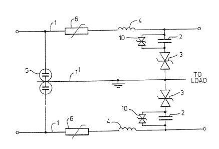
Figure 4 shows a modification of the circuit shown in figure 1
which will provide protection to a circuit against DC overvoltages.
This circuit corresponds to that shown in Figure 1 with the addition of
a further bidirectional voltage clamping diode 10 connected across the
capacitor 2. The clamping diode 10 has a breakdown voltage such that
the sum of the breakdown voltages of the two diodes 3 and 10 is greater
than the maximum system voltage.