Note: Descriptions are shown in the official language in which they were submitted.
2~92882
BACKGROUND OF THE INVENTION
The present invention is directed to a circuit arrangement
having a switching amplifier, particularly for hearing aids, for
limiting a pulse-width-modulated signal that is formed by a low-
frequency signal and a higher-frequency delta signal.
German Patent 36, 16 752 discloses a circuit arrangement
having a switching amplifier for hearing aids. In this known
switching arrangement, a pulse-width-modulated signal is formed
from a low-frequency audio signal and from a higher-frequency delta
signal in a pulse duration modulator. After amplification of the
pulse-width-modulated signal in the switching amplifier, the audio
signal is detected from the different duration of the individual
pulses of the pulse-width-modulated signal. This usually occurs in
hearing aids on the basis of the low-pass effect of an earphone
connected to the output of the switching amplifier.
In a pulse-width-modulated signal, the amplitude of the audio
signal (useful signal) is coded in the width of the individual
pulses of the pulse-width-modulated signal that controls the
switching amplifier. The amplitude of the useful signal coded in
the pulse width can therefore not be limited in the output stage
(in the switching amplifier) with standard methods or clip
circuits.
The audio signal (useful signal) has therefore already been
limited in amplitude in a preliminary stage and a pulse-width
modulation has been generated with this previously limited audio
signal. As a result thereof, however, an undesirable spectral
spread of the useful signal already occurs before the pulse width
modulator. This results in undesirably high back-convolution
products (high distortions) in the output signal.
.. . . .
.-, ::
: .
.. . . . .
2~92~8~2
In order to avoid this disadvantage, the operating voltage (or
the operating current) for the switching amplifier has already been
limited. This, however, leads to an undesirable reduction in gain
and power of the demodulated output signal.
S MMARY OF THE INVENTION
It is an object of the present invention to provide a circuit
arrangement of the species initially cited with which a limitation
of the output signal (useful signal) of the switching amplifier is
achieved without a reduction in gain and with only slight
distortions.
This object is achieved by a circuit arrangement having a
switching amplifier for limiting a pulse-width-modulated signal
that is formed from a low-frequency signal and a higher-frequency
delta signal. The pulse-width-modulated signal is supplied to a
limiting circuit which shortens the width of individual pulses in
the pulse-width-modulated signal whose width, is greater than a
maximum pulse width prescribable with the limiting circuit.
Alternatively, or in addition thereto, the pulse-width-modulated
signal is supplied to a limiting circuit which lengthens the width
of individual pulses in the pulse-width-modulated signal whose
width is shorter than a minimum pulse width prescribable with the
limiting circuit. The pulse-width-modulated signal, that is
modified by the limiting circuit, is supplied to the switching
amplifier as an input signal.
The invention is based on the perception that the amplitude of
the useful signal is contained in every pulse width of the pulse-
width-modulated signal. In a circuit arrangement of the present
invention the pulse width of the individual pulses in the pulse-
width-modulated signal is varied (decreased or increased) when a
maximum value or minimum value is reached. That is, the maximum or
.,: -: .
~a~2~2
minimum width of the individual pulses is modified (limited) in the
pulse-width-modulated signal. What this inventive limitation
(modification) effects is that the pulse-width-modulated signal can
be amplified in the switching amplifier without a reduction in gain
and without additional distortions in the low-frequency signal
(useful signal) arising before or during the amplification in the
switching amplifier. These equivalent solutions can be
alternatively utilized for switching amplifiers that do not operate
in push-pull fashion. Both solutions can be utilized in common for
push-pull circuits.
For limiting the maximum possible width of the individual
pulses, the pulse-width-modulated signal is inventively supplied to
a circuit, for example a gate circuit, that is preferably fashioned
as an AND circuit. The maximum permitted width of individual
pulses is prescribed with the gate circuit. When the pulse-width-
modulated signal has individual pulses whose width is longer than
the maximum width prescribed with the gate circuit, then these
individual pulses are limited to the maximum permitted width in the
gate circuit. The switching amplifier is driven with the pulse-
width-modulated signal limited in this manner.
In a development of the present invention, a square-wave
signal that defines the maximum permitted pulse width at the gate
circuit is formed from the higher-frequency delta signal and from
a threshold voltage with a comparison circuit. The delta signal
used for generating the pulse-width-modulated signal is thus also
inventively used for forming a gate pulse for defining the maximum
permitted pulse width. As a result thereof, a symmetrical
limitation of the individual pulses to be limited in the pulse-
width signal is achieved without complicated circuit technology.
What this means is that every limited individual pulse (viewed
~" ~ , ~ 1' ' ' ' ''
- : . ~ : .
2~g28~
proceeding from an imaginary center line of the individual pulse,
the center line being perpendicular the time axis) is shortened by
an amount of approximately the same size at both sides in the
direction of this time axis. Distortions that can arise after the
demodulation of the limited, low-frequency signal (useful signal),
given asymmetrical limitation of the individual pulses in the
pulse-modulated signal, are avoided or at least considerably
diminished by this symmetrical shortening (limitation) of the width
of an individual pulse.
Further advantageous developments of the present invention are
as follows.
A control signal for the limiting circuit is formed from the
high-frequency delta signal, and the limiting circuit is composed
of a gate circuit.
The pulse-width-modulated signal is supplied to a first input
of a first AND circuit that forms the limiting circuit. A square-
wave signal is formed from the higher-frequency delta signal and
from a threshold voltage with a comparison circuit. The square-
wave signal is supplied to a second input of the first AND circuit
that has its output side coupled to an input of the switching
amplifier.
The pulse-width-modulated signal is supplied as an inverted
signal to a first input of a second AND circuit that forms the
limiting circuit. Another square-wave signal is formed with a
further comparison circuit from the higher-frequency delta signal
and from another threshold voltage. This other square-wave signal
is supplied to a second input of the second AND circuit that has
its output side coupled to another input of the switching
amplifier.
.
.: ~
, .
2~2~2
The AND circuit can be coupled to the switching amplifier via
a flip-flop circuit. The comparison circuit can be a comparator
circuit whose inverting input has the delta voltage supplied to it
and whose non-inverting input has the threshold voltage supplied to
it.
The threshold voltage is supplied to the comparison circuit
via a preferably digitally programmable final control element. An
input of one comparison circuit is connected via the final control
element to an input of the other comparison circuit. The inputs of
the comparison circuits connected via the final control element are
each coupled to a respective terminal of an operating voltage
supply of the circuit arrangement.
The circuit arrangement can be an integrated circuit or a
component part of an integrated circuit.
BRIEF DESCRIPTION OF THE DRAWINGS
The features of the present invention which are believed to be
novel, are set forth with particularity in the appended claims.
The invention, together with fu~ther objects and advantages, may
best be understood by reference to the following description taken
in conjunction with the accompanying drawings, in the several
Figures of which like reference numerals identify like elements,
and in which:
FIG. 1 is a circuit arrangement for the inventive limitation
of a pulse-width-modulated signal;
FIG. 2 is an inventive circuit arrangement for limiting
complementary pulse-width-modulated signals; and
FIG. 3 is an illustration of a few signals that can occur in
inventive circuit arrangements of FIG. 1 and/or of FIG. 2.
~'
:'
' ,
2~92~8~
DESCRIPTION OF THE PREFERRED EMBODIMENT
FIG. 1 shows a schematic hearing aid circuit having a circuit
arrangement of the present invention. An audio signal picked up by
a microphone 1 is converted into electrical, low-frequency signal
and is supplied to a pulse-width modulator 3 via an amplifier 2.
A delta signal that is higher in frequency in comparison to the
low-frequency signal is supplied to the pulse-width modulator 3
from a generator 4 that can also have pulse-shaping stages (not
shown). A pulse-width-modulated signal that is supplied to a gate
circuit 5 via a first input 6, is formed in the pulse-width
modulator 3 in a known way from the low-frequency signal and from
the delta signal. Individual pulses in the pulse-width-modulated
signal are limited in width with the gate circuit 5 insofar as
their width is greater than a width prescribable by the gate
circuit 5.
In this exemplary embodiment, the gate circuit 5 is an AND
circuit and receives a control signal via a second input 7. This
control signal is formed in a comparison circuit 8. The delta
signal supplied by the generator 4 is additionally employed for the
formation of the control signal. To that end, the delta signal is
compared to a prescribable, for example, manually settable
threshold voltage in the comparison circuit 8. Comparators are
particularly suitable for use as a comparison circuit. A square-
wave control signal for the gate circuit 5 is then available at the
output of the comparison circuit 8.
The pulse width of the individual pulses in the square-wave
control signal can then be varied by an adjustable threshold
voltage that is supplied via a terminal 9 of the comparison circuit
8. The width for the pulse-width-modulated signal is controlled in
the gate circuit 5 with this variable setting of the threshold
2~2~2
voltage. Consequently, the size of the limitation of the pulse
width of the pulse-width modulated signal can be controlled with
the threshold voltage at the comparison circuit 8. A switching
amplifier lo, to which an earphone 11 is connected in a known way,
is driven with the pulse-width signal limited by the gate circuit
5.
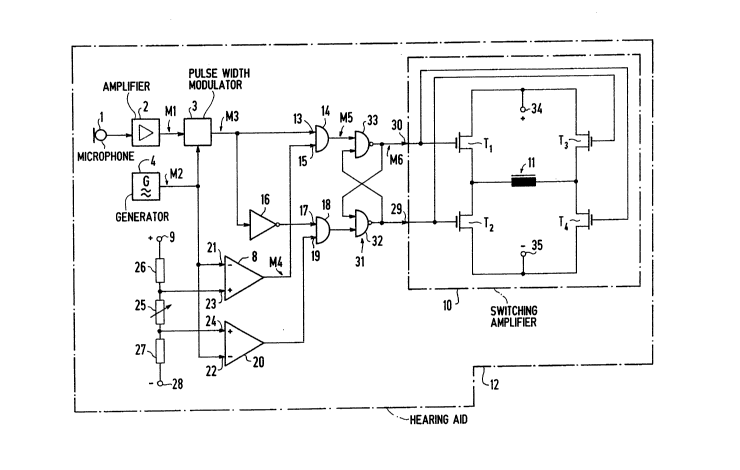
FIG. 2 shows a circuit arrangement of the invention which has
further circuit parts in addition to the circuit parts set forth in
FIG. 1 and, in particular, is suitable for a symbolically
illustrated hearing aid 12 whose switching amplifier lo operates in
push-pull fashion. To facilitate an understanding of the circuit
arrangement, FIG. 3 shows a few signals that can be measured within
this circuit arrangement at the measurement points respectively
referenced Ml...M6.
A low-frequency signal S1 can be measured at a measuring point
Ml in FIG. 2 between the amplifier 2 and the pulse~width modulator
3; FIG. 3 shows a portion of this low-frequency signal Sl with
rising amplitude. The generator 4 in FIG. 2 supplies a delta
signal S2 shown in FIG. 3 at the measuring point M2. A pulse-
width-modulated signal S3 that can be measured at the measuring
point M3 at the output of the pulse-width modulator 3 derives from
the processing of the signals Sl and S2 in the pulse-width
modulator 3. This pulse-width-modulated signal S3 is supplied via
a first input 13 (FIG. 2) to a gate circuit fashioned as first AND
circuit 14. The first AND circuit 14 has a control signal supplied
to it on a second input 15 from the comparison circuit 8 that has
already been set forth in detail in FIG. 1. The control signal is
a square-wave and can be measured at measuring point M4 in FIG. 2:
it is shown as a square-wave signal S4 in FIG. 3.
,
,
~,
-- 2~92~
It may be derived from FIG. 3 that the pulse-width-modulated
signal S3 has individual pulses, for example Il, I2, having
different pulse widths Dl and D2. In the case of the control
signal S4, all individual pulses have respectively the same pulse
width D3. The maximally permitted pulse width of the individual
pulses and the pulse-width-modulated signal S3 is limited to the
pulse width D3. FIG. 3 shows such a limited, pulse-width-modulated
signal S5. This signal is measurable at the measuring point M5 at
the output of the AND circuit 14 (FIG. 2). It may be derived from
the limited pulse-width signal S5, shown in FIG. 3, that the
individual pulse I1 in the signal S3 has the same width Dl as the
corresponding pulse in the limited signal S5. The individual pulse
Il, consequently, has remained unlimited. By contrast, the pulse
I2 in the unlimited signal S3 is limited to the maximum permitted
width D3 in the limited signal S5 (chronologically shortened).
In FIG. 2, the circuit arrangement of the present invention is
fashioned for push-pull operation. To that end, the pulse-width-
modulated signal S3 is supplied as an inverted signal via an
invertor 16 to a first input 17 of a second AND circuit 18 that
operates as an gate circuit. The second AND circuit is supplied
with a square-wave signal via a second input 19, this square-wave
signal representing a complementary signal with resp~ct to the
square-wave signal S4. This complementary square-wave signal is
formed in a further comparison circuit 20 from a comparison of the
higher-frequency delta signal S2 to a different threshold voltage.
The different threshold voltage is thereby set complementary to the
threshold voltage at the comparison circuit 8. As a result
thereof, the critical advantage derives that the demodulated low-
frequency signal is symmetrically limited, i.e. the positive and
negative amplitudes are limited proceeding from the same amount
28~2~2
with reference to an average value (symmetry line). Consequently,
the distortions are again reduced as a consequence of this
symmetrical limitation.
In a development of the present invention, the two comparison
circuits 8 and 20 are fashioned as comparator circuits to whose
inverting inputs 21 and 22 the delta voltage (the delta signal) S2
is supplied. A non-inverting input 23 at the comparison circuit 8
and a non-inverting input 24 are connected to one another via a
final control element 25, for example a potentiometer. The inputs
23 and 24 connected via the final control element 25 are thereby
coupled to a respective terminal (positive or negative) of the
circuit arrangement. The coupling to the positive terminal in the
circuit arrangement of FIG. 2 occurs via a resistor 26 and the
terminal 9. The coupling to the negative terminal occurs via a
resistor 27 and a terminal 28. The resistors 26 and 27 can be
matched to the final control element 25 such that the limitation of
the pulse-width signal can be switched on and off with the final
control element 25. The final control element 25 can also be a
digitally settable and/or programmable final control element.
As a result, a limited pulse-width signal is likewise
available at the output of the AND circuit 18, whereby (by contrast
to the limited signal S5, see FIG. 3) the pulse width D4 of a short
individual pulse is increased to a minimum value D5 in the signal
S6. The pulse width D5 is not downwardly transgressed, whereby the
minimum value D5 can be prescribed by the gate circuit that is AND
circuit 18. The minimum permitted pulse width of the individual
pulses in the pulse-width-modulated signal that is complementary to
the signal S3 is consequently limited with the AND circuit 18. The
limited and pulse-width-modulated push-pull signals generated in
this way are available at the output side at the AND circuits 14
.
': ' : .~.. ' .:: ~,
2~923~.~
and 18 for coupling to an input 29 or 30 of the switching amplifier
10 .
In a development of the present invention, a flip-flop circuit
31 having two trigger circuits 32 and 33 is provided for the
coupling of the AND circuits 14 and 19 to the switching amplifier
10. In the case of a limitation of the pulse width, a balancing of
the two signals at the inputs 29 and 30 of the switching amplifier
10 is required in the case of a limitation of the pulse width.
Distortions can thereby be diminished again. FIG. 3 shows such a ;^
limited and balanced pulse-width modulated signal S6 that can be
measured at the measuring point M6 in FIG. 2.
In FIG. 10, the switching amplifier 10 has four MOSFET
transistors Tl through T4 working in switched mode. The
transistors Tl and T2 as well as the transistors T3 and T4 are
respectively fashioned complementary relative to one another. The
switching amplifier 10 is supplied with operating voltage via
terminals 34 and 35. As a result of the switched mode, either of
the transistors Tl and T4 or T3 and T2 are simultaneously
conductive. The time span within which these transistors are
conductive is controlled by the respective pulse width of each and
every pulse in the limited, pulse-width signal supplied via the
inputs 29 and 30 of the switching amplifier. Consequently, given
a change of the level in the pulse-width signal, the activated
transistors change into the non-conductive condition and the
transistors that were previously non-conductive are thus activated.
As a result the earphone 11 arranged in the bridge arm of the
switching amplifier 10 is switched between the operating voltage
(positive and negative terminals) at the terminals 34 and 35. The
limitation arises due to the shortening of, for example, an
originally long individual pulse having a width D2 to having a
. : i
- 2~92~2
width D3 (in this respect, see the signals S3 and S5 in FIG. 3).
As a result of an individual pulse shortened in this way, the
current or the voltage can no longer form at full magnitude at the
earphone 11. As a result thereof, the low-frequency signal
reproduced by the earphone 11 appears as an amplitude-limited
signal.
As a result of the digital limitation of a low-frequency
signal present here, no additional noise arises, the levels are
reproducible and are digitally programmable and readable. The
circuit has a more beneficial efficiency than known pre-stage
limitation circuits. As a result of its structure, the circuit
arrangement of the present invention can also be fashioned as an
integrated circuit or as a component part of an integrated circuit.
It is also advantageous that no loss in gain arises for low
amplitudes. Moreover, with a simple auxiliary circuit a digital
display signal that indicates the response of the limitation (clip
effect) can also be derived.
The invention is not limited to the particular details of the
apparatus depicted and other modifications and applications are
contemplated. Certain other changes may be made in the above
described apparatus without departing from the true spirit and
scope of the invention herein involved. It is intended, therefore,
that the subject matter in the above depiction shall be interpreted
as illustrative and not in a limiting sense.
: : .