Note: Descriptions are shown in the official language in which they were submitted.
3 ~ 4 ~
FREQUENCY SYNTHESIZER USING PHASE-LOCKED LOOP
BACKGROUND OF THE INVENTION
1. Field of the Invention
The present invention relates to a frequency
synthesizer using phase-locked loop (will be termed
"PLL" hereinafter).
2. Description of the Prior Art
Fig. 4 shows in block diagram a conventional
PLL frequency synthesizer disclosed in the publication
"Basics and Applications of PLL", written by Teruo
Kadota, published by the Publication Department of the
Electric College of Tokyo. In the figure, reference
numeral 1 denotes a fixed-frequency oscillator, 2 is a
frequency divider which divides a constant frequency
generated by the oscillator 1 to produce a reference
phase signal fr, and 3 is a phase comparator which
compares an output phase signal fp of a programmable
frequency divider 7 with the reference phase signal fr
and uses the comparison output to control a charge pump
4. Indicated by 5 is a low-pass filter (will be termed
"LPF" hereinafter) which smoothes the output of the
charge pump 4, and 6 is a voltage-controlled variable-
frequency oscillator (will be termed "VCO" hereinafter).
ZO ~30 40
, _
.
The programmable frequency divider 7 divides the output
frequency of the VCO 6 to produce the phase signal fp.
Next, the conventional PLL frequency
synthesizer arranged as described above will be
explained. The fixed-frequency oscillator 1 has its
output fed to the frequency divider 2, by which the
oscillation frequency is divided. For the reference
phase signal (reference frequency) fr of the frequency
divider 2 and the frequency division factor N of the
programmable frequency divider 7, the phase signal fO
produced by the VCO 6 is related with the phase signal
fp produced by the programmable frequency divider 7 as:
fO = fp x N.
The phase comparator 3 controls the charge
pump 4 to have a high output impedance when fp is equal
to frl to have a positive output voltage (supply
voltage) when fp is higher than frl or to have a ground
voltage when fp is lower than fr. The LPF 5 is formed
of a lag-lead filter, RC filter, active filter, or the
like, and it smoothes the output of the charge pump 4.
The smoothed output is fed to the VCO 6. The VCO 6 is
designed to raise or lower its output frequency in
response to an increase or decrease, respectively, of
the input voltage (output voltage of LPF 5).
~'.
_ - 3 - ~ ~
- In the case of fr = fo/N~ the charge pump 4 is
in the high output impedance state, causing the LPF
output to be unvaried, i.e., the input voltage to the
VCO 6 is unvaried and it does not vary the output
frequency, and the relation fr = fo/N is kept unchanged.
In the case of fr ~ fo/N~ the charge pump 4
produces a positive output voltage, which is applied to
the LPF 5, causing it to supply an increased voltage to
the VCO 6. Consequently, the output frequency of the
VCO 6 rises, and the value of fo/N increases.
In the case of fr < fo/N~ the charge pump 4
produces a ground (zero) voltage, which is applied to
the LPF 5, causing it to supply a decreased voltage to
the VCO 6. Consequently, the output frequency of the
VCO 6 falls, and the value of fo/N decreases.
Accordingly, a negative feedback loop is
formed for the phase of the signal, and the operation
settles when the output frequency of the VCO 6 becomes
equal to N times the output frequency (reference
frequency) of the frequency divider 2, i.e., fO = fp x
N.
The phase comparator 3 operates continuously
even in the steady state (the programmable frequency
divider 7 has a constant division factor N and the VCO 6
has a constant output frequency). It is not possible to
~'
- 4 -
maintain a constant output voltage Vf of the LPF, but
instead the voltage Vf continues to fall due to the
power loss of the resistive components of the LPF 5,
which is a ~-connection of resistors R1, R2 and R3 and
capacitors C1 and C2 for example as shown in Fig. 5.
The VCO frequency also falls continuously, and
the charge pump 4 operates to charge the LPF 5 by
producing a positive voltage. As a result, the VCO 6 is
always subjected to a pulse modulation at the reference
frequency (this phenomenon will be termed "reference
leak" hereinafter).
Fig. 6 shows the reference phase signal fr by
(a) and the phase signal fp by (b) for the output phase
signal fO of 500 MHz and frequency division factor N of
10000, as an example, in the steady state, resulting in
a comparator output fpD of 50 kHz, for example, as shown
by (c), and a small reference leak R is created. The
transition of the output phase signal fO following a
change in the frequency division factor of the
programmable frequency divider from N to M until the
steady state is restored is generally called "step
response".
As described above, the conventional PLL
frequency synthesizer implements the phase comparison at
the reference frequency, imposing a pulse modulation at
- _ - 5 - ~ ~
- the reference frequency on the VCO 6. Therefore, it is
necessary for the LPF 5 to have a low cutoff frequency.
Moreover, the output step response following a change in
the frequency division factor of the frequency divider
until the settlement of steady state is deteriorated.
SUMMARY OF THE INVENTION
A first object of the present invention is to
provide a PLL frequency synthesizer in which the pulse
modulation at the reference frequency (reference leak)
imposed on the VCO is diminished.
A second object of the present invention is to
provide a PLL frequency synthesizer in which the
settlement of step response is sped up.
In order to achieve the above objects, the
inventive PLL frequency synthesizer is designed to
operate on multiple reference phase signals produced
from a reference phase signal by shifting the phase.
The output phase signal of the VCO is compared with
these multiple reference phase signals. Accordingly,
the frequency of pulse modulation increases apparently,
implementing an increased number of phase comparison,
and the reference leak is reduced. The LPF can have
higher cutoff frequency, and the settlement of step
response is sped up.
In accordance with one aspect of the present
invention there is provided a frequency synthesizer
using phase-locked loop for producing signals of
- 5a -
multiple frequencies, comprising: a voltage-controlled
oscillator which generates a signal having a frequency
correspondent to an input voltage supplied thereto; a
reference signal oscillator which generates a first
reference phase signal that establishes an operational
base of said synthesizer; a phase distributor which
produces a predetermined number of second reference
phase signals based on the first reference phase signal,
phases of the second reference phase signals being
different each other; a predetermined number of
frequency dividers for dividing an output frequency of
said voltage-controlled oscillator; a predetermined
number of phase comparators for detecting phase
differences between the predetermined number of second
reference phase signals and outputs of the predetermined
number of frequency dividers respectively and for
producing phase difference signals which represent the
detected phase differences; an adder which adds the
phase difference signals produced by the predetermined
number of phase comparators; a charge pump which varies
an output state thereof in response to an output of said
adder; and a low-pass filter which removes high-
frequency components above a predetermined frequency
from an output signal of said charge pump and supplies a
resulting voltage signal to said voltage-controlled
oscillator.
In accordance with another aspect of the
present invention there is provided a frequency
~'
O ~
synthesizer using on phase-locked loop for producing
signals of multiple frequencies, comprising: a voltage-
controlled oscillator which generates a signal having a
frequency correspondent to an input voltage supplied
thereto; a reference signal oscillator which generates a
first reference phase signal that establishes an
operational base of said synthesizer; a phase
distributor which produces a second reference phase
signal and a third reference phase signal based on said
first reference phase signal; a first frequency divider
which divides an output frequency of said voltage-
controlled oscillator by a first frequency division
factor; a second frequency divider which divides an
output frequency of said voltage-controlled oscillator
by a second frequency division factor; a first phase
comparator which detects a phase difference between the
second reference phase signal and an output signal of
said first frequency divider to produce a first phase
difference signal which represents the detected phase
difference; a second phase comparator which detects
phase difference between the third reference phase
signal and an output signal of said second frequency
divider to produce a second phase difference signal
which represents the detected phase difference; an adder
which adds the first and the second phase difference
signals; a charge pump which varies an output state
thereof in response to an output of said adder; and a
low-pass filter which removes high-frequency components
,~ '
- 5c - ~ O ~ ~ ~ 4 ~
above a predetermined frequency from an output signal of
said charge pump and supplies a resulting voltage signal
to said voltage-controlled oscillator.
- 6 -
BRIEF DESCRIPTION OF THE DRAWINGS
Fig. 1 is a block diagram showing the PLL
frequency synthesizer based on an embodiment of this
invention;
Fig. 2 is a timing chart showing the signals
at various portions of the circuit arrangement of Fig.l;
Fig. 3 is a timing chart showing the signals
at various portions of the circuit arrangement of Fig. 1
of the case where the output phase signals of the
programmable frequency dividers are out of phase with
each other;
- Fig. 4 is a block diagram showing the
conventional PLL frequency synthesizer;
Fig. 5 is a schematic diagram of the low-pass
filter used in the circuit arrangement of Fig. 4; and
Fig. 6 is a timing chart showing the signals
at various portions of the circuit arrangement of Fig.
4.
DESCRIPTION OF THE PREFERRED EMBODIMENTS
Embodiments of the present invention will be
described in detail with reference to the drawings.
_ 7 _ ~ O ~ ~ ~ 4
Fig. 1 shows in block diagram the arrangement
of the PLL frequency synthesizer based on an embodiment
of this invention.
Embodiment 1:
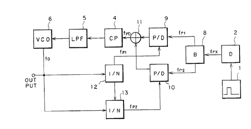
In Fig. 1, reference numeral 1 denotes a
fixed-frequency oscillator, 2 is a frequency divider
which divides a constant frequency generated by the
oscillator 1 to produce a reference phase signal f
and 8 is a phase distributor which produces pulse
signals frl and fr2 of different phases using the
reference phase signal frx. The difference of the
phases is a full wavelength of the reference phase
signal frx as shown by (a), (b) and (c) in Fig. 2.-
Indicated by 9 and 10 are phase comparatorswhich compare output phase signals produced by
programmable frequency dividers 12 and 13 which will be
explained shortly. The phase comparator 9 compares the
output phase signal fpl shown by (d) in Fig. 2 with the
reference phase signal frl to produce an output signal
shown by (f). The phase comparator 10 compares the
output phase signal fp2 shown by (d) with the reference
phase signal fr2 to produce an output signal shown by
(g). These phase comparators 9 and 10 produce the
output signals alternately as shown by (f) and (g).
- Indicated by 11 is an adder which adds the
output signals of the phase comparators 9 and 10, 4 is a
charge pump which varies its output state in response to
the output of the adder 11, 5 is a low-pass filter (LPF)
which smoothes the output of the charge pump 4, and 6 is
a voltage-controlled oscillator (VCO).
The programmable frequency divider 12 produces
the pulse signal fp1 at counts N, 2N, 3N, ... pieces of
fO as in the case of the conventional frequency
synthesizer, while the programmable frequency divider 13
is designed to produce the pulse signal fp2 at counts
3N/2, 5N/2, 7N/2, ... pieces of fO. The reference phase
signal frx of the frequency divider 2 is set equal to
2fr~ where fr is a reference phase signal in the
conventional PLL frequency synthesizer shown in Fig. 4.
Next, the operation of the frequency
synthesizer of this embodiment will be explained. This
PLL frequency synthesizer has two frequency feedback
circuits dealing with signals that are out of phase by a
half wavelength as mentioned above, and therefore frx is
equal to 2fr in the steady state. Then, dfrl/dt is equal
to dfr2/dt and equal to dfr/dt, and all of fr1/ fr2 and fr
are the same frequency.
Accordingly, provided that the system is
stable initially, it can be stable continuously merely
through the provision of two frequency feedback circuits
-~ ~ 9~
dealing with signals that are out of phase by a half
wavelength as shown by (b)-(g) in Fig. 2.
In addition, the implementation of phase
comparison on a multiple-stage basis (two stages in this
embodiment) reduces the phase shift at each comparison
operation, resulting in a smaller reference leak for the
reference frequency fr as compared with the conventional
PLL frequency synthesizer. The phase comparison of the
signals out of phase by a half wavelength results in a
reference leak with a frequency twice the reference
frequency fr as shown by (h) in Fig. 2, allowing the LPF
5 to have a lower cutoff frequency, and the settlement
of step response speeds up. The implementation of phase
comparison more than once in the transitional state
speeds up the settlement of step response as compared
with the conventional PLL frequency synthesizer.
Embodiment 2:
The PLL frequency synthesizer based on an
other embodiment of this invention will be explained.
In the preceding embodiment, the programmable
frequency divider 13 may not produce pulse outputs at
counts 3N/2, 5N/2, 7N/2, and so on in some cases by some
reason. This embodiment is intended to let the
programmable frequency divider produce pulse outputs at
counts X, X + N, X + 2N, and so on, where X is an
~0 ~3~ ~
-- 10
integer nearest to N/2, and consequently the reference
leak can be reduced and the settlement of step response
can be sped up as in the preceding embodiment.
In case the programmable frequency divider 13
has a frequency division factor of 10001 for example,
the reference phase signals fr1 and fr2 are out of phase
with each other by a half wavelength exactly in the
steady state as shown by (b) and (c) in Fig. 3. The
output phase signals fp1 and fp2 are out of phase with
each other by a half wavelength plus a half period of fO
as shown by (d) and (e), and accordingly the output
signals PD1 and PD2 of the phase comparators 9 and 10 are
out of phase with each other by a half wavelength plus a
half period of fO as shown by (f) and (g). As a result,
the adder 11 produces an output phase signal fpD as
shown by (h). The output phase signal fpD has a
frequency approximately equal to 100 kHz. This
embodiment based on the scheme of approximation is
adopted when the first embodiment described previously
cannot be applied, e.g., when the frequency division
factor is 10001 and a 5000.5 wavelengths cannot be
counted.
~,,