Note: Descriptions are shown in the official language in which they were submitted.
wo 92/07444Pcr/us9l/o623s
., ' 393~'31
SIDE PANEL SIGNAL PROCESSOR FOR A
WI~ESCREEN TELEYlS~ON SYSTEM
This invention concerns apparatus for processing the
5 side panel information component of a widescreen television
signal containing main and side panel components~
A conventional television system, such as a system in
accordance with the NTSC broadcast standard adopted in the
United States and elsewhere, processes a television signal
10 representative of an image with a 4:3 aspect ratio (the ratio of the
width to lhe height of a displayed image). Recently, there has
been interest in using higher aspect ratio images for tetevision
systems, such as 5:3, 16:9 and 2:1, since such higher aspect ratios
more nearly approximate or equal the aspect ratio of the human
15 eye compared to the 4:3 aspect ratio of a standard television
display . Advanced television systems for producing 5 :3 nspect
ratio images are described, for example, in U.S. patent 4,816,899 -
Strolle, et al. and in U.S. patent 4,855,811 - Isnardi. In these
systems side panel image information is encoded by time
2 0 compressing low frequency side panel luminance and
chrominance information into horizontal overscan regions, and
high frequency side panel luminance and chrominance
informalion are encoded by time expansion and modulation of an
auxili~ry subcarrier. The side panel luminance information
2 5 compG~lent (Y) and the side panel chrominance color difference
information components (I and Q) are each processed separa`tely
before being encoded.
Separate processing of the side panel luminance
component, the side panel "I" color difference component and the
3 0 side panel "Q" color difference component advantageously permits
each component to be uniquely tailored with respect to one or
more desired factors such as noise reduction, gain, or filter
characteristics for example. Illustratively, in the case of a
wides.,leerl television signal which ia int~r,ded to ~c .,ompatlblG
35 with a standard NTSC receiver, gain factors could be individually
adjusted to assure that side panel information encoded in a
broadcast NTSC compatible signal will not produce visible
interference in a standard receiver display. Also, the type of
noise reduction system employed could be optimized based upon
.
wo 92/07~44 Pcr~US91/o6239
2-
,~ ~
~he characteristic of the particular component, e.g., based upon
whether or not a given component contains DC information.
It is herein recognized, however, that it can be
beneficial to process certain side panel components together as a
5 combined signal before encoding, particularly in a system
employing cornplementary noise reduction apparatus at the
transmitter encoder and receiver decoder. Specifically, it is
recognized herein ~hat bandwidth restrictions on certain
components such ~s side panel components can lead to unwanted
10 bnnd-edge crosstalk between such components. That is,
bandwidth limitations may not permit practical filters from
keeping the components sufficiently separated at their band edges
to prevent significant crosstalk. This crosstalk can significantly
impair the effectiveness of the encoder/decoder noise reduction
15 apparatus, which to be most effective requires that the signal
processed by the decoder noise reduction apparatus be essentially
the same signal processed by the encoder noise reduction
apparatus, except for transmission noise which the noise reduction
apparatus is intended to reduce. It is also recognized hcrein that
2 0 non-linearities generated by non-linear noise reduction apparatus
can create harmonics which can adversely affect the quality of a
reconstitu~ed imnge signal when such componen~s are processed
in separate signal paths with separate noise reduction~ apparatus.
The disclosed apparatus according to ~he principles of the present
2 5 invention addresses these concerns. In addition to exhibiting a
simplified configuration, the disclosed apparatus significantly
reduces the impact of the described crosstalk and non-linearities
in a reconstituted image signal.
In accordance with the principles of tlle present
3 0 invention, first and second components of a widescreen video
signal are combined at an encoder before being subjected to noise
reduction and encoding processes. At a decoder, the combined
signal is subjected ~o noise reduction processing before bein~
separated into its constituent components and decoded. In an
3 5 illustrated preferred embodiment of the invention, side panel high
frequency luminance information and a side panel color difference
information component are combined and processed as a
combined signal by a noise reduction encoder, time expander and
wo s2/07444 .~ ~ 3 ~ PCr/US91/06239
filter before modulating an auxitiary subcarrier. After
demodulation at a decoder, the combined signal is filtered, time
compressed and processed by a noise reduction unit before being
separated into its constituent components.
Btief~çscriDtion of the Drawing
FIGURE l shows a portion of an NTSC compatible
wide~creen transmitter/encoder including apparatus according to
the present invention.
l O FIGURE 2 shows a portion of an NTSC compatible-
widescreen receiver/decoder including apparatus according to the
present invention.
FIGURE 3 shows an additional portion of the
receiver/decoder of FIGURE-2.- --
FIGURE 4 shows additional details of the disclosed
apparatus.
FIGURES 5 and 6 are block diagrams of video signal
compansion (noise reduction) networks used in the arrangements
of E;IGURES 1 and 2 respectively.
FIGURE 7 illustrates a plurality of compander
characteristics which may be implemented in an adaptive
compander.
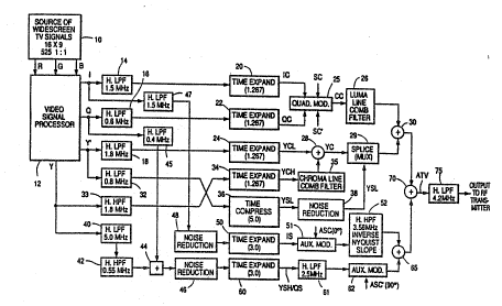
In ~he NTSC compatible widescreen
transmitter/encoder of FIGURE 1, a widescreen television s1gnal
source 10, such as a color television camera, provides a 16x9 wide
aspect ratio 1:1 progressively scanned (non-interlaced) television
signal with color components R, G and B. These signals are
processed by a video signal processor 12 to provide luminance
output signals Y, Y' and color difference output signals I and Q.
. 30 Processor 12 includes circuits for translating the R, G, B input
signals to Ii Q, Y format, verlical-temporal filters for pre-filtering
each of the I, Q, Y signals, and progressive scan to interlaced scan
converters for each of the I, Q, Y signals. Output signals I, Q and Y
, from processor 12 are 262 line progressive scan signals. An
35 output signal Y' is a 52S line interlaced luminance signal.
Encoding of the main (i.e., "center") panel information
will be discussed first. Color diffe-ence signals I, Q and luminance
signal Y' from unit 12 are respectively filtered by filters 14, 16
wo 92/0~ PCr/US91/06239
4 -
and 18 before being time expanded by units 20, 2'~ and 24,
respectively. Units 20, 22 and 24 exhibit a time expansion factor
of 1.267 and operate only on the center (main) panel portion of
the 1, Q, Y' signals from filters 14, 16 and 18. Thus time
S expanders 20 and 22 respectively provide output center panel
color difference signals IC and QC. Time expander 24 provides an
output luminance center panel low frequency signal YCL. Signals
IC and QC quadrature modulate 3.58 MHz quadrature phased
subcarriers SC and SC' in a modulator 25 to produce a modulated
10 center panel chrominance signal CC. This signal is processed by a
luminance line comb filter 26 to remove luminance information
before being applied to a center panel chrominance input of an
adder 30.
The center panel luminance signal input to ~dder 30 is~
15 developed as follows. The Y luminance signal from processor 1 2 is
high pass filtered by a unit 33 and time expanded by a unit 34,
which operates only during the center panel interval, to develop a
center panel high frequency luminance signal YCH. This signal is
processed by a chrominance line comb filter 35 to rernove
2 0 chrominance information before being combined with center
panel low frequency luminance signal YCL in adder 28 to produce
a center panel luminance signal YC.
Expanded center panel luminance signal YC is spliced,
~o compressed side panel low frequency luminance information
25 YSL by means of a multiplexer 29. Briefly, as discussed in detail
in U.S. patent 4,855,811 - Isnardi, signal YSL constitutes time
compressed low frequency left and right side panel luminance
information which is placed in left and right horizontal overscan
regions of the center panel signal by means of multiplexer 29.
. 30 Signal YSL is obtained by filtering signal Y' from processor 12 by
means of a 0.8 MHz horizontal low pass filter 32, then selectively
time compressing the side p~nel portions of the filtered signal by
means of a compressor 36 which operates only during the side
panel intervals. Signal YSL from compressor 36 is processed by a
3 5 noise reduction unit 38 of the type shown in FIGURE ~ for
improving the signal-to-noise characteristic of signal YSL before
being applied to splicer 29. The output of multiplexer/splicer 29
is applied to Ihe luminance input of center panel signal combiner
:
.
- -~
- - . :. ~
WO 92/07444 h jJ ~ 3 '~ Pcr/us9l/o6239
30. Noise reduction unit 38, as well as noise reduction uni~s 46
and 48, are amplitude compansion units having similar
complementary counterpart units with inverse operating
characteristics at a receiver.
High frequency side panel information is processed as
follows. The "I" color difference component from processor 12 is
filtered by a 1.5 MHz low pass filter 47 to produce a wideband I
signal, and is processed by noise reduction unit 48. The output
signal from unit 48 is time expanded during side panel intervals
by a time expander 50 to produce wideband side panel color
difference component IS. This signal is applied to an auxiliary
modulator 51 for amplitude modulating an auxiliary subcarrier
ASC with a nominal 0 phase. Subcarrier ASC exhibits a frequency
of 3.58 MHz, the frequency of the standard cllrominance
subcarrier, but exhibits a phase which inverts from field-to-field
unlike the standard chrominance subcnrrier. Specifically, the
phase of signal ASC inverts every 262 horizontal lines (262H).
The modulated signal from uni~ 51 is applied to a 3.58
MHz horizontal high pass filter 52 having an inverse Nyquist
slope. Pilter 52 mirrors a filter at a receiver having a Nyquist
slope to acllieve a desired amplitude response at a receiver
demodulator. Specifically, the cascade of inverse Nyquist slope
filter 52 at the encoder with a complementary Nyquist slope filter
a~ a receiver decoder (as will be seen in FIGURE 2) produces a
2 5 desired flat amplitude response for high frequency side panel
luminance signal YSY when demodulated at the receiver. Such
cascade of Nyquist slJpe filters also assures that modulated
auxiliary subcarrier ASC exhibits symmetrical double sideband IS
information so that proper quadrature demodulation is achieved
3 0 at the decoder, i.e., so that signal IS maintains a desired phase
characteristic and does not crosstalk into components YSH or QS.
Side panel high frequency luminance information and
side panel color difference component "Q" are combined for
processing. The Q output signal from processor 12 is conveyed via
a 0.4 MHz horizontal low pass filter 45 to a combiner 44, where it
is combined wi~h signal Y from unit 12 after fil~ering by a S.O MHz
horizontal low pass filter 40 and a 0.55 MHz horizontal high pass
filter 42. The output signa! from combiner 44 is processed by
WO 92/07444 PCI-~US91/06239
<~, ; ' - 6 -
noise figduction unil 46 and afterwards time expanded by a unit
60. Expander unit 60 operates during the side panel intervals for
producing combined side panel highs signal YSH/QS, i.e., side panel
high frequency luminance information combined with side panel Q
5 color difference information. Because time expander 60 is not
ideal, low energy repeat spectra are generated above 2.5 MHz.
Low pass filter 61 removes these repeat spectra and prevents
them from cross-talking into the main (center) panel component
after modulation.
Combined signal YSH/QS is coupled via a 2.5 MHz
horizontal low pass filter 61 to an auxiliary modulator 62, which
modulates ~n auxili~ry 3.58 MHz subcarrier ASC' with the output
signal from filter 61. Subcarrier ASC' is in ph~se quadra~ure with
subcarrier ASC and~exhibits a similar phase inversion from field to
15 field. The output signal from modulator 62 and ~he output signal
from filter 52 are combined by an adder 65. An adder 70
combines the output signals from adders 30 and 65 to produce a
compatible widescreen advanced television signal ATV. This
signal is low pass filtered by a 4.2 MHz filter 75 to restrict signal
20 ATV to the standard NTSC channel ~andwidth before being
applied to an RF transmitter for broadcast.
F1GURE 2 shows a portion of a widescreen television -~
recei~er including apparatus for decoding the widescreen ATV
signal generated by the arrangement of FIGURE 1. A received
25 baseband encoded ATV signal (e.g., from an RP tuner and
demodulator assembly not shown) is applied to a 1.6 MHz
horizont~l high pass filter 210, the output of which is applied to
an intraframe processor 212. Processor 212 averages (additively
combines) and differences (subtractively combines~ image lines
3 0 262H apart within frames above 1.6 MHz to recover high
frequency main panel signal information at an output AVG.
Modulated side panel high frequency information is provided at a
differencing output DIFF of processor 212.
The main panel component from the AVG output of
3 5 processor 212 is filte~ed by a horizontal line comb filter 214 to
provide separated luminance (Y) and chrominance (C) output
components. The separated main panel luminance component is
time compressed by a unit 220, which operates only during the
..
. ~ .
wo 92J07444 Pcr/US91/o6239
7 ~ u 9 3 i~ 3 i
main panel interval, to restore separated main panel component Y
to its original spatial relationship. The time compressed signal
from unit 220 is then filtered by a 5.0 MHz horizontal low pass
filter 222 tO de~lop main (center) panel luminance high
5 frequency component YCH. The separa~ed main panel
cllrominance inform~tion (C) is quadrature demodulated by a
demodulator 2 l 5 responsive to quadrature phased reference
signals SC and SC' h~ving the frequency and phase characteristics
of corresponding subcarrier signals provided at ~he
10 encoder/transmitter. Demodulated center panel I and Q color
difference components IC and QC are horizontally low pass filtered
by filters 216 and 218 respectively before being time compressed
by units 217 ~nd 219. Time compression units 217 and 219
operate during the center panel intervals to restore~ the 'original
15 spatial relationship of signals IC and QC.
The cen~er panel low frequency luminance information
is restored to its original form by means of filter 225 and time
compressor 228. Horizontal low pass filter 225 passes frequencies "'
of input signal ATV which are below about 1.6 MHz to time
2 0 compressor 228, which operates during the center panel interval
to restore low frequency center panel luminance information to its
original spatial relationship, as signal YCL.
The input ATV signal is also applied to a noise
reduction unit 230, which exhibits the complementary operating
25 characteristics of unit 38 in the encoder of FIGURE 1. A time
expander 232 operates during ~he side panel intervals to restore
~he original spatial format of the side panel information which had
been time compressed and placed in the horizontal overscan
regions. The ou~put signal from expander 232 is processed by a
30 0.8 MHz horizontal low pass filter 234 to provide low frequency
side panel luminance signal YSL in its original spatial form.
To recover side panel I color difference component IS,
the signal from the DlPF output of processor 212 is demodulated
by an auxiliary demodulator 240 whish responds to an auxiliary
3 5 reference signal ASC having the same frequency and phase
characteristics as subcarrier ASC developed at the encoder. The
demodulated signal from unit 240 is filte, red by a 1.0 MH~
horizontal low pass filter 242, time compressed during side panel
,
wo 92r0744~ ' PCr~US9I/06239
- 8 -
intervals by a unit 244 to restore the original spatial format of the
signal component, and processed by a noise reduction unit 246 to
produce side panel color I difference component IS. Noise
reduc~ion unit 246 Dnd unit 46 at thc encoder exhibit
5 complementary operating characteristics.
To recover side panel components YSH and QS, the
signal from the DIFF output of processor 212 is processed by a
3.58 MHz horizontal low pass Nyquist slope filter 250 before being
demodulated by auxiliary demodulator 252. With regard to the
10 use of Nyquist filter 250 it is noted that in this example
component QS is a double sideband signal modulation component
of auxiliary subcarrier ASC' occupying 3.38 MHz to 3,79 MHz, and
component YS~i is a (lower) single sideband modulation
- component of auxiliary subc~rrier ASC' occupying 1.78 MHz to
15 3.25 MHz. Imparting a Nyquist slope to the higher energy double
sideband region of the combined YSH/QS modulaled signal (from
3.08 MHz to 4,08 MHz) reduces the effectiYe energy of the double
sideband region by one-half, so that a flat demodulation
amplitude respanse results over the auxiliary subcarrier
20 modulation frequencies, Demodulator 252 also responds to an
auxiliary reference signal ASC' having the same frequency and '
phase characteristics as auxiliary subcarrier ASC' developed at the
encoder. A demodulated output signal from demodulator 252
contains combined YSH and QS components and is filtered by a 2.5
2 5 MHz horizont~l low pass filter 254.
The output signal from filter 254 is time compressed
by a unit 256 which operates during side panel intervals to
restore the original spatial rel~tionship of Lhe combined YSHIQS
side panel information, The time compressed signal is then
3 0 processed by a noise reduction uni~ 258, which exhibits the
complementary operating characteristics of unit 46 in the encoder
system of FIGURE 1. The output signal from noise reduction unit
258 is separated into the YSH and QS components by means of a
0.55 MHz horizontal high pass filter 260, and a 0.4 MHz horizontal
3 5 low p~ss filter 261, respectively.
The described processing of side panel components QS
and YSH as a combined signal results in ~ less complicated system
with improved performance, Fewer noise reduction modules, time
- - . . ~ ~ . . .-
. . . : . .~ ,- -: -,
'
wo 92/0~ PC~/US91/06239
compressor/expander units and modulators are needed. The
hardware savings are especially significant in the case of a
decoder in a consumer, television receiver. Performance is
improved because no intermediate band-ed~e filtering occurs
S between the noise reduction unit at the decoder. That is, there
are no intermediate filters which would change the shape of the
signal waveform applied to the decoder noise reduction network,
c~using the decoder noise reduction network to mistrack relative
to the encoder noise reduction network. The 0.55 MHz lower cut-
10 off frequency of signal YSH is determined by filter 42 inFIGURE l, and the 0.4 MHz upper cut-off frequency of signal QS is
determined by filter 45 in FIGURE 1. Furthermore, processing the
QS and YSI~ components as a combined sign~l means that ~ny
crosstalk or harmonics- associated with non-linear noise reduction ~
operation at the encoder are more effectively cancelled at the .-
decoder.
More specifically, the output of adder 44 contains
signal QS in a low frequency band and signal YSH in a relatively
higher frequency band, with frequency overlap in the region
20 0.3 MHz - 0.65 MHz. When the output signal of adder 44 is passed
through encoder noise reduction unit 46, the nonlinear transfer
function of noise reduction unit 46 causes harmonics of signal QS
lo develop. These harmonics crosstalk into signal YSH. Because
signal QS//YSH remains intact as a combined signal until after
25 processing by a noise reduction unit at the decoder (i.e., unit 258
in FIGURE 2), these crosstalk harmonics can be removed by the
inverse nonlinear transfer function exhibited by the decoder noise
reduction unit.
If signals YSH and QS were processed by separate
30 noise reduction systems, harmonics generated by the QS encoder
noise reduction unit would be filtered out by the QS lowpass filter
at the decoder. The lost harmonics would cause mistracking in the
QS decoder noise reduction unit, resulting in inferior performance.
The QS h~rmonics, now residing in the YSH signal as crosstalk,
35 compromise the performance of the YSH decoder noise reduction
unit as well.
The output signals developed by the decoder
appllr;ltus of FlaURE 2 are processed further as shown in FIGURE
- ,:
wo 92~07444 ~ Pcr/US91/o6239
- 10-
3. Signals IC and IS, QC and QS, YCH and YSH, and YCL and YSL are
respectively spliced by splicers 321, 322, 323 and 324
respectively. Output signals from splicers 323 and 324 are
combined by an adder 326 to provide a restored widescr~en
5 luminance signal with main panel and side panel information. The
widescreen chrominance signals from splicers 321 ~nd 322 and
~he widescreen luminance signal from adder 326 are conver~ed
from interlaced to progressive scan format by means of
converters 330-332 before being converted to analog form via a
1 0 digital-to-analog converter unit 335. Widescreen analog signals I,
Q, Y are matrixed and processed by conven~ional video signal
processing circuits in a network 338 to produce color image
representative signals R, G and B suitable for display by a
- ~ -- widescreen image reproducing device 340.~~
1 5 FIGURE 4 depicts apparatus suitable for generating
quadrature phased signals SC and SC', and quadrature phased
auxiliary signals ASC and ASC'. A signal generator 410 provides a
3.58 MHz sinusoidal signal SC at a nominal 0 phase. This signal is
phase shifted 90 by a network 412 to produce signal SC'. Signal
20 ASC is derived from signal SC by means of a field phase control
unit 414, which produces auxiliary signal ASC with a phase that
reverses from field to field relative to the phase of a standard
chrominance subcarrier, A 90 phase shifter 415 produces
auxiliary signal ASC' in phase quadrature with auxiliary signal
2 5 ASC,
FIGURE 5 illustrates a video signal adaptive
compander network suitable for use as noise- reduction networks
38, 46 and 48 in FIGURE 1.
Typic~lly compandors (at the transmitting end of a
' 30 system) expand the amplitude of low amplitude signals and
compress the amplitude of higher amplitude signals to improve
the signal-to-noise ratio, Such a process enhances ~he quality of
the lower level signals, but does l;~tle to improve higher level
signals. On the other hand, if the relative amplitude of the signal
3 5 to be processed is known, the signal-to-noise ratio of signals of
almost any level can be improved by adaptive companding. This
is accomplished by selecting a companding transfer characlerislic
which has its grea~est slope located in the range of amplitudes in
- :
wo svo7444 Pcr/uS9l/o6239
I 1 2 ~' ~9 3 2 ~''3 1
whicl~ signal samples are e~pected to occur. Consider the
companding curves illustrated in FIGURE 7, which are applicable
for a compandor implemented in the transmitting end of a
companding system. It will be appreciated ~hat by changing the
axis designation from Input and Output to Output and Input, the
curves will correspond to the inverse or receiving end
companding curves. If the amplitude of the input signal is
expected to be between, e.g., 80 and 100 IRE, signals in this range
will be expanded. and lesser amplitude signals will be
1 0 compressed. Alternatively, if the signal is expected to be 50 IRE,
signals in the range of about 50 +10 IRE will be expanded and
signals of greater and lesser amplitude will be compressed. A
syslem which opera~es in this manner is an amplitude tracking
- companding system. The high ~ correlation of video signals from
1 5 line-to-line, field-to-field, or frame-to-frame permits the
realization of such a tracking companding system.
In FIGURE 5, video signal to be companded is applied to
a multicharacteristic compandor 500 which provides a companded
signal to be transmitted at the terminal OUTPUT. Cornpander 500
2 0 may be a ROM programmed with a plurality of tables of transfer
characteristics, each table defining one companding characteristic
such as those illustrated in FIGURE 7. The selection of the
particular table used at any given time is determined by a control
signal developed by the compandor control circuit 580.
The companded signal is also coupled to inverse
companding circuitry including elements 5 t 0-580 which emulates
the expansion circuitry at the receiving end of the transmission
system. An expanded signal from compandor 510 is applied to a
first signal prediction circuit including elements 520-523 and to a
3 0 second signal prediction circuit including elements 530-536.
The second prediction circuit includes the cascade
arrangement of a delay element 530 which delays signal by
substantially one ~ideo frame period minus one horizontal line
period, and delay elements 531 and 532 each of which delay
signals by one llorizontal line period. Video signals from delay
elements 530, 531 and 532 are coupled to signal weighting
circuits 535, 534 and 533 respectively. Weighting circuits 535,
534 and 533 scale the signals applied thereto by factors 114, 1/2
w~ 92~07444 ,~ PCr/US91/06U9
~ .- ~, .,
~. - I 2-
and 1/4 respectively. Video signal from weighting circuits 533-
535 are summed in an adder circuit 536 which generates a
prediclion signal lemporally relaled to the currenl video signal.
The lemporal prediclion signal from adder 536 is coupled lo a
5 variable weighting circuit 542 which scales the lemporal
prediclion signal by a variable factor K provided by a conlrol
signal generator 560.
The temporal prediction signal may include
contributions from the current image. This is indicated by the
10 broken arrow connection between the OUtpUl of compandor 510
and adder 536. This connection indicates that signal from one or
more picture poinls of lhe current image frame may be weighted
and combined wilh signals from the previous frame.
The first prediction circuit develops a prediction signal
15 from signal from the current image field. In FIG~lRE 5, output
signal from compandor 510 is delayed by one horizontal line
period minus time T in delay element 520. The time T is a short
time period typically equal to onè quarter of the period of the
color subcarrier or a multiple thereof. The delayed signal is
2 0 further delayed by cascade connected delay elements 521 and
522, each of which provides a del~y of period T. Delayed signals
from delay elements 520-522 are coupled to scaling ~nd
combining circuitry 523, which develops a spati~l prediction
signal. Scaling and sombining circuitry 523 may be simil~r to
2 5 elements 533-536 of the temporal prediction circuit. The spatial
prediction signal provided by elemen~ 523 is coupled to a variable
weighting circuit 540, which scales the spatial prediction signal by
a variable factor (I-K) provided by control circuit 560.
For non-moving images, or areas of images which
30 contain no interframe motion, the temp~ral average tends ~o be a
more accurate prediction of the current signal. For moving
images, or areas of images that contain interframe motion, the
spatial average tends to be a more accurate prediclion of the
current signal. In order that the system perform well for both
3 5 conditions of image motion and non-motion, the expanded signal
from compandor 510 is monitored for motion to enable selection
of the appropriate predi~tion signal.
,
,
. . , .:
.,- ~ ~ :
wo gv07444 ~ ~, n ~ ~ 3 L Pcr/us9t/o6239
A motion detector 550 is coupled between the input ~o
delay element 530 and the ou~put of delay elemenl 531. Motion
detec~or 550 provides a signal corresponding to interframe image
signal differences. This difference signal is coupled to control
S signal gener~tor 560 which generates variable control signals K
for particular ranges of the difference signal. For image areas
containing no motion, i.e., when the difference signal provided by
motion detector 550 is zero, the control signal generator provides
a K value of unity. In this instance weighting circuits 542 and 540
are respectively conditioned to pass the temporal prediction and
to exclude the spatial prediction. When motion detector 550
generates a large amplitude difference signal, indic~ting
signific~nt image motion, generator 560 provides a v~lue K of
zero, which conditions weig~ting circuits 540 and 542 to pass the
spatial prediction to tlle exc3usion of the temporal prediction. For
intermediate valued image difference signals, generator 560
develops values of K between zero and unity, which values of K
condition weighting circuits 540 and 542 to pass the spatial and
temporal prediction signals in complementary proportions.
2 0 The weighted spatial and temporal prediction signals
from weighting circuits 540 and 542 are coupled to an adder 544
which provides a sum corresponding to lhe desired prediction
signal. The prediction signal is coupled through a conventional
coring circuit 570 to compandor control circuit 580. Compandor
2 5 control circuit 580 responds to the prediction signal from adder
544 for developing appropriate control signnls to condition
compandors 500 and 510 to operate according to a particular one
of i~s selectable transfer charac~eristics.
FIGURE 6 illustrates companding circuitry for the
3 0 receiving end of a system which incorpora~es the companding
circuitry of FIGURE 5 at the transmitting end. Elements
designated witb Iike numerals as elements in the Fli3URE 5
apparatus are similar and perform like functions. The apparatus
of FIGURE 6 is suitable for use as noise-reduction networks 230,
3 5 246 and 258 in Fl(:iURE 2.
- :,. . ' ' -