Note: Claims are shown in the official language in which they were submitted.
The embodiments of the invention in which an exclusive
property or privilege is claimed are defined as follows:
1. In a display device having a matrix of matrix
points arranged in columns and lines, each of said matrix
points comprising four partial image points of different
colors distributed on two half-columns and two half-lines,
each of said partial image points formed by a light-emitting
end of an optical fiber illuminated in color, each of said
light- emitting ends being coverable and uncoverable by a
bistable flap controllable with an electromagnet in a pulsed
manner, and each of said electromagnets of said bistable
flap controllable with a setting and a setting reference
potential for uncovering each of said ends of said optical
fibers and with a return and a return reference potential
for covering each of said ends of said optical fibers by a
control device in accordance with display information
selected from a memory device,
the improvement comprising:
in each of the columns (x1 ... xn), each of the
electromagnets (Kx11y11; Kx11y12; Kx12y11; Kx12y12; ...) of
the flaps being sequentially triggerable in said half-
columns by a column control device (SpSt); in a first
partial step, a reset reference potential (+) being applied
and, in a second partial step, a set reference potential
(ground) being applied to the respectively triggered half-
column (x11, x12); and
each of said electromagnets (Kx11y11; Kx11y12;
Kx12y11; Kx12y12; ...) of the flaps being triggerable
parrallel in each of the lines (yl ... ym) by a line control
device (ZSt); in the first partial step of column
triggering, the reset potential (ground) being applied to
all half-lines (y11, y12 ... ym1, ym2) and, in the second
partial step of the column triggering, a respective partial
11
display information (TInf) corresponding to the triggered
half-column (x11, x12 ... xn1, xn2) being applied as set
potential (+) to the corresponding half-lines (y11, y12 ...
ym1, ym2).
2. In a display device having a matrix of matrix
points arranged in columns and lines, each of said matrix
points comprising four partial image points of different
colors distributed on two half-columns and two half-lines,
each of said partial image points formed by a light-emitting
end of an optical fiber illuminated in color, each of said
light- emitting ends being coverable and uncoverable by a
bistable flap controllable with an electromagnet in a pulsed
manner, and each of said electromagnets of said bistable
flap controllable with a setting and a setting reference
potential for uncovering each of said ends of said optical
fibers and with a return and a return reference potential
for covering each of said ends of said optical fibers by a
control device in accordance with display information
selected from a memory device,
the improvement comprising:
in each of the columns (x1 ... xn), each of the
electromagnets (Kx11y11; Kx11y12; Kx12y11; Kx12y12; ...) of
the flaps being sequentially triggerable in half-columns by
a column control device (SpSt); in a reset cycle, a reset
reference potential (+) being applied to the respective
triggered half-column (x11, x12 ... xn1, xn2) and, in the
course of each column triggering, a reset potential (ground)
being simultaneously applied by a line control device (ZSt)
to all half-lines (y11, y12 ... ym1, ym2); and
in a set cycle, the electromagnets (Kx11y11;
Kx11y12; Kx12y11; Kx12y12; ...) of the flaps sequentially
12
triggerable with a set reference potential (ground) in said
half-columns (x11, x12 ... xn1, xn2) by said column control
device (SpSt); in the course of each column triggering, the
respective partial display information (TInf) corresponding
to the triggered half-column (x11, x12 ... xn1, xn2) being
applied to the corresponding half-lines (y11, y12 ... ym1,
ym2) as the set potential (+).
3. In a display device in accordance with claim
1,
wherein
each of said half-lines (y11, y12 ... ym1, ym2)
has a reset line (y11r, y12r ...) and a set line (y11s,
y12s...),
each of said reset lines (y11r, y12r ...) is
connected to one of the connectors of all electromagnets
(Kx11y11; Kx11y12; Kx12y11; Kx12y12; ...) of the flaps of
the corresponding half-line (y11, y12 ... ym1, ym2) through
at least one rectifier (Dr) which conducts one of the reset
potential (+) and the reset potential (ground),
each of said set lines (y11s, y12s ...) is
connected to one of the connectors of all electromagnets
(Kx11y11; Kx11y12; Kx12y11; Kx12y12; ...) of the flaps of
the corresponding half-line (y11, y12 ... ym1, ym2) through
at least one rectifier (Ds) which conducts one of the set
potential (ground) and the set potential (+),
the other connectors of the electromagnets
(Kx11y11; Kx11y12; Kx12y11; Kx12y12; ...) of the flaps are
connected to corresponding half-columns control lines, and
the column control device (SpSt) has a column
reset switch (rhsp1, rhsp2, ...) for each of said half-
columns and a column set switch (shsp1, shsp2, ...) for such
13
of said half-columns and the line control device (ZSt) has a
line reset switch (rhz1, rhz2, ...) for each of said half-
lines and a line set switch (shz1, shz2, ...) for each of
said half-lines.
4. In a display device in accordance with claim
1,
wherein
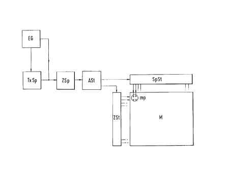
the column control device (SpSt) and the line
control device (ZSt) are triggerable by a display control
device (ASt) to which the display information is supplied
form a memory (ZSp) in the form of partial display
information for each of said half-columns.
5. In a display device in accordance with claim
4,
wherein
said memory (ZSp) comprises the display
information in said half- columns (x11, x12 ... xn1, xn2)
and said half-lines (y11, y12 ... ym1, ym2) as values "0"
and "1", the value "1" corresponding to setting the
electromagnets (Kx11y11; Kx11y12; Kx12y11; Kx12y12; ...) of
the corresponding flap into the incovered position.
14
6. In a display device in accordance with claim
4,
wherein
for the display information embodied as a text,
the matrix (M) is divided into a plurality of equal fields
(B1, B2, B3, B4 ...), the size of said fields being adapted
to the display of a letter, and
the partial display information associated with
the letters is taken form the memory (ZSp) by the control of
a text memory (TxSp).
7. In a display device in accordance with claim
3,
wherein
the column control device (SpSt) and the line
control device (ZSt) are triggerable by a display control
device (ASt) to which the display information is supplied
form a memory (ZSp) in the form of partial display
information for each of said half-columns.
8. In a display device in accordance with claim
7,
wherein
said memory (ZSp) comprises the display
information in said half- columns (x11, x12 ... xn1, xn2)
and said half-line (y11, y12 ... ym1, ym2) as values "0"
and "1", the value "1" corresponding to setting the
electromagnets (Kx11y11; Kx11y12; Kx12y11; Kx12y12; ...) of
the corresponding flap into the uncovered position.
9. In a display device in accordance with claim
7,
wherein
for the display information embodied as a text,
the matrix (M) is divided into a plurality of equal fields
(B1, B2, B3, B4 ...), the size of said fields being adapted
to the display of a letter, and
the partial display information associated with
the letters is taken from the memory (ZSp) by the control of
a text memory (TxSp).
10. In a display device in accordance with claim
8,
wherein
for the display information embodied as a text,
the matrix (M) is divided into a plurality of equal fields
(B1, B2, B3, B4 ...), the size of said fields being adapted
to the display of a letter, and
the partial display information associated with
the letters is taken from the memory (ZSp) by the control of
a text memory (TxSp).
11. In a display device in accordance with claim
2,
wherein
each of said half-lines (y11, y12 ... ym1, ym2)
has a reset line (y11r, y12r ...) and a set line (y11s,
y12s...),
each of said reset lines (y11r, y12r ...) is
connected to one of the connectors of all electromagnets
(Kx11y11; Kx11y12; Kx12y11; Kx12y12; ...) of the flaps of
the corresponding half-line (y11, y12 ... ym1, ym2) through
16
at least one rectifier (Dr) which conducts one of the reset
potential (+) and the reset potential (ground),
each of said set lines (y11s, y12s ...) is
connected to one of the connectors of all electromagnets
(Kx11y11; Kx11y12; Kx12y11; Kx12y12; ...) of the flaps of
the corresponding half-line (y11, y12 ... ym1, ym2) through
at least one rectifier (Ds) which conducts one of the set
potential (ground) and the set potential (+),
the other connectors of the electromagnets
(Kx11y11; Kx11y12; Kx12y11; Kx12y12; ...) of the flaps are
connected to corresponding half-colums control lines, and
the column control device (SpSt) has a column
reset switch (rhsp1, rhsp2, ...) for each of said half-
columns and a column set switch (shsp1, shsp2, ...) for each
of said half-columns and the line control device (ZSt) has a
line reset switch (rhz1, rhz2, ...) for each of said half-
line and a line set switch (shz1, shz2, ...) for each of
said half-lines.
12. In a display device in accordance with claim
2.
wherein
the column control device (SpSt) and the line
control device (ZSt) are triggerable by a display control
device (ASt) to which the display information is supplied
form a memory (ZSp) in the form of partial display
informtion for each of said half-columns.
17
13. In a display device in accordance with claim
12,
wherein
said memory (ZSp) comprises the display
information in said half- columns (x11, x12 ... xn1, xn2)
and said half-lines (y11, y12 ... ym1, ym2) as calues "0"
and "1", the value "1" corresponding to setting the
electromagnets (Kx11y11; Kx11y12; Kx12y11; Kx12y12; ...) of
the corresponding flap into the incovered position.
14. In a display device in accordance with claim
12,
wherein
for the display information embodied as a text,
the matrix (M) is divided into a plurality of equal fields
(B1, B2, B3, B4 ...), the size of said fields being adapted
to the display of a letter, and
the partial display information associated with
the letters is taken from the memory (ZSp) by the control of
a text memory (TxSp).
15. In a display device in accordance with claim
13,
wherein
for the display information embodied as a text,
the matrix (M) is divided into a plurality of equal fields
(B1, B2, B3, B4 ...), the size of said fields being adapted
to the display of a letter, and
the partial display information associated with
the letters is taken from the memory (ZSp) by the control of
a text memory (TxSp).
18
16. In a display device in accordance with claim
11,
wherein
the column control device (SpSt) and the line
control device (ZSt) are triggerable by a display control
device (ASt) to which the display information is supplied
from a memory (ZSp) in the form of partial display
information for each of said half-columns.
17. In a display device in accordance with claim
16,
wherein
said memory (ZSp) comprises the display
information in said half- columns (x11, x12 ... xn1, xn2)
and said half-line (y11, y12 ... ym1, ym2) as values "0"
and "1", the value "1" corresponding to setting the
electromagnets (Kx11y11; Kx11y12; Kx12y11; Kx12y12; ...) of
the corresponding flap into the incovered position.
18. In a display device in accordance with claim
16,
wherein
for the display information embodied as a text,
the matrix (M) is divided into a plurality of equal fields
(B1, B2, B3, B4 ...), the size of said fields being adapted
to the display of a letter, and
the partial display information associated with
the letters is taken from the memory (ZSp) by the control of
a text memory (TxSp).
19
19. In a display device in accordance with claim
17,
wherein
for the display information embodied as a text,
the matrix (M) is divided into a plurality of equal fields
(B1, B2, B3, B4 ...), the size of said fields being adapted
to the display of a letter, and
the partial display information associated with
the letters is taken from the memory (ZSp) by the control of
a text memory (TxSp).