Note: Descriptions are shown in the official language in which they were submitted.
209L3986
Technical Field
The invention concerns a device for parallel-serial conversion of N
synchronous data streams.
The use of optical transmission paths is preferred in large
telecommunication networks, because of their special quality characteristics,
such
as e.g. high transmission capacity, low damping and no crosstalk. Several
subscriber connections are routed through an optical transmission path
(optical
waveguide), e.g. by the frequency multiplex process or the time multiplex
process.
The article "16 Gbit/s Fibre Transmission Experiment using Optical
Time-Division Multiplexing" by R. S. Tucker et al., published in "Electronics
Letters", 1987, Vol. 23, No. 24 on pages 1270 and 1271, documents an optical
time multiplex system. In it, four parallel electrical data streams are
converted by
optical senders and Ti:Li Nb 03 modulators into four parallel optical data
pulse
streams. The optical senders are time-displacement-controlled by electrical
time
delay elements (quarter bit-period time delays) in such a way, that the
parallel
optical data pulse streams are converted without overlapping into an optical
waveguide in a space multiplex stage (MUX). The recovery of the four
electrical
data streams at the end of the optical waveguide is done by means of a
demultiplexer stage (DEMUX), which contains cascaded optical directional
coupler
switches. Four optical receivers are installed downstream of the demultiplexer
stage.
The introduced optical time multiplex system is self contained. The
conversion of the electrical data streams by means of transmitter-switching
and
receiver-switching to the optical waveguide takes place at its beginning or
its end.
~ It is not possible to integrate the transmitter-switching and the receiver-
switching into any section of a given optical transmission path.
It should also be possible to attach as many data sources and data outputs
as possible to an optical transmission path, when they are located
individually or
in groups in different sections of the transmission path. This problem occurs
particularly in ring structure transmission systems or in large scale
switching
2
2093986
networks, such as ATM systems. The publication "N'i'T Review", 1991, Vol. 3,
No. 2, on pages 98 - 101 of the article "Photonic Switching Technologies . ..
" by
K. Yukimatsu et al., introduces a high speed optical ATM network with a
transmission speed of about 1 Tbit/s.
Iri it, the ATM cells of several parallel data inputs are compressed in time
and then are interlaced without overlapping and transmitted through an optical
time
multiplex path.
At the end, the compressed ATM cells are assigned to parallel data
outputs by means of cell selectors, and are expanded in time to their original
form
by means of cell buffers. The article does not provide sufficiently clear
technology, particularly in the depiction of the "cell" elements, in which
inconsistencies between text and drawing occur. Still, it can be seen in
principle
that the transmission of data takes place in cells in the time multiplex
process, and
that neither the transmitter-switching on the input side, nor the receiver-
switching
on the output side, can be integrated into any section of a given optical
transmission path.
mmarv of the ~nven
The present invention has the task of coupling and uncoupling several
2 o synchronous data streams into or out of any section of an optical
transmission
path.
According to the present invention, there is provided
an apparatus (100, 100') for converting N synchronous data
streams (I1, I2,..., IN) having a constant data pulse width
(PW) from parallel to serial form for -injection into an
optical communication link (OCOM) by means of the following
functionally cooperating elements:
(1) N optical modulators (OMOD) contained in the optical
communication link (OCOM);
30 (2) each of the N optical modulators (OMOD) being
controlled by one of the N synchronous data streams
3
...
.
;: ::
2093986
(I1, I2,..., IN) via a respective switching element
(TS) ;
(3) each of the respective switching element (TS) being
clocked by a synchronous timing signal having a timing
pulse with a timing interval (TI) for reducing the
constant data pulse width (PW) to the time interval
(TI) which is not greater than the Nth fraction of the
constant data pulse width;
(4) so that the N synchronous data streams are, according
to ( 2 ) and ( 3 ) , converted into a serial data sequence
(Dn) of short optical pulses (D1, D2,..., D4) for
injection into the optical communication link (OCOM),
and
(5) each of the N optical modulators (OMOD) is followed by
one of at least N-1 optical delay elements (OTD; OTD1,
OTD2,...) which ensure nonoverlapping serial injection
of the short optical pulses (D1, D2,..., D4) into the
optical communication link (OCOM).
According to the present invention, there is also
provided an apparatus (200) for converting a serial data
stream (DS) to N parallel data streams (Il, I2,..., IN),
said serial data stream (DS) representing a bit
interleaving arrangement of the N parallel data streams
(I1, I2,..., IN) and being carried on an optical
communication link (OCOM), by means of the following
functionally cooperating elements:
(1) at least one optical branching element (OSP) contained
in the optical communication link, so that N optical
branches (OPL1, OPL2,..., OPLN) diverge therefrom;
(2) each of N optical modulators (OMOD) each followed by a
pulse stretcher (PEX) that is coupled to a respective
,, 4
2093986
one of the optical branches, each of the N optical
modulators (OMOD) being clocked by a synchronous
timing signal, and
(3) N-1 optical delay elements (OTD).each connected to a
respective one of the optical branching elements (OSP)
to ensure a parallel selection of the N parallel data
streams (I1, I2,..., IN) from the serial data stream
(DS) by means of the N optical modulators (OMOD).
Thus, with respect to the first mentioned device, the data streams are
routed by means of parallel-serial conversion to an optical transmission path.
~~n~y~ ~e parallel-serial conversion takes place with optical modulators and
optical time delay elements, which operate together in such a way, that the
insertion of N data streams occurs in accordance with a shift register with N
parallel inputs.
The optical modulators form the light in the optical transmission path
(optical signal carrier) as a function of the data streams. Accordingly the
device
in claim 1 can also be understood to be an optical shift register with N
parallel
inputs, one serial optical input and one serial optical output. Depending on
the
modulator control, the parallel data streams can be both electrical and
optical in
nature. The device can be integrated into any section of an optical
transmission
path, because the coupling of the data streams takes place without the aid of
additional optical transmitters, rather it takes place by means of optical
modulators. Thus, in principle, no interruption of the optical transmission
path is
taking Place.
With respect to the second mentioned device, the N data streams are
recovered by serial-parallel conversion of one serial data stream passing
through
the optical transmission path. The serial-parallel conversion essentialiy
takes place
by means of optical expanders and optical time delay elements, which make
e~.
~vr
'fa:.r' ~ ~..~~~
...~~"-~..
4a
2093986
parallel decoupling of the N data streams from the optical transmission path
possible. Accordingly, and analogously to the latter argument, the device can
also
be understood to be an optical shift register with N parallel outputs, one
optical
serial input and one optical serial output.
This device can also be integrated into any section of an optical
transmission path, since the optical expanders do not represent any
interruption of
the optical transmission path, in principle.
With respect to the first mentioned device, it can be coupled by means of
the modulators into any section of the optical transmission path, which can,
for
example, represent a high speed optical waveguide ring. The optical
transmission
path already contains intermittent optical data pulses, such as can occur in
asynchronous packet switching systems. The device is therefore a technical
variation in the manner of a switchable drop-in multiplexer. Thus, data
streams
can be advantageously coupled into any section of the optical waveguide ring
during time intervals in which no packet traffic takes place.
The device can also be constructed in accordance with a type of multiplex
transmitter. The optical transmission path is supplied with a constant light
(optical
carrier), which is formed by the optical modulators at the beginning. The
constant
light is emitted by a semiconductor laser, for example, and is coupled into an
optical waveguide, after modulation.
5
... 2093986
Brief Descri ion of the Drawin;gc
The following explains the invention in more detail, by referring to
configuration examples, and by means of the enclosed drawings.
Figure 1 shows a device according to an optical, switchable drop-in
multiplexer;
Figure 2 shows a device according to an optical multiplex transmitter;
Figure 3 shows a device according to an optical, switchable drop-out
multiplexer;
Figure 4 shows pulse-time diagrams with respect to the parallel-serial
conversion.
Best Mode for Carrving out the Invention
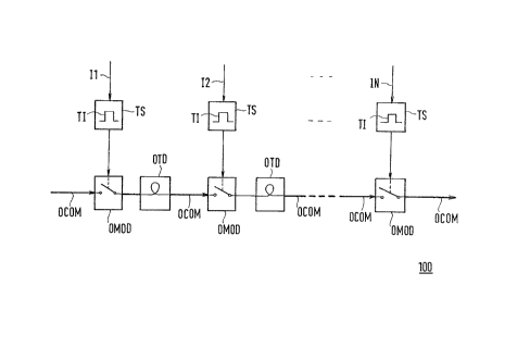
The circuit in figure 1 contains N optical modulators OMOD, which are
represented by Ti:Li Nb 03 switches with an electrical control input each.
Also shown are N-1 optical time delay elements OTD, each of which
consists of an optical waveguide loop with a predetermined signal running
time,
and N electrical switching elements TS, each consisting of a logic AND-gate,
controlled by one of the data streams and one asymmetrical timing signal with
a
switch time interval TI.
Starting with one of the optical modulators, these and the optical time
delay elements are switched on alternately and are thereby integrated in
series into
a section of an optical waveguide OCOM. Each optical modulator forms a
switching unit, in conjunction with the coupled electrical switching element
and
the optical time delay element connected downstream of the modulator.
Inserting other such basic units into the above described series circuit
makes a modular expansion of the circuit in figure 1 possible. The now
constant
signal running times of the optical waveguide loops are added into a total
delay
time. This is not longer than the Nth part of the (N-1)th time of the constant
data
pulse width of the synchronous data streams. The switching time interval is
not
longer than the signal running time.
6
209398b
The above determinations and a blank control of the optical modulators
ensure the use of the device in figure 1 as a switchable time multiplex stage.
This
is described more concretely below for the instance of a coupling of four
synchronous data streams (N=4), where figure 4 is also referenced.
Each of the four data streams il, ..., I4 represents an electrical ATM
signal, which has a constant data pulse width PW of 7.1 ns e.g.,
(corresponding to
a transmission speed of 140 Mbit/s). The four data streams are synchronous to
each other, and each is routed to a switching element. This consists of a
logic
AND-gate with an input for the respective data stream and a second input for a
timing signal.
Synchronously with data streams, the timing signal contains a timing
pulse with a time interval TI, which corresponds to the fourth part of the
data
pulse width. This blanks out the respective data pulses Ax, Bx, Cx, ... of the
ATM signals down to the fourth part of the original data pulse width PW.
In each case, one optical Ti:Li Nb 03 switch that is controllable in inverse
logic (active low) converts the shortened electrical data pulses into
respectively
short optical pulses Dl, ..., D4, in the partial section of an optical ATM
high
speed optical waveguide ring OCOM. The latter operates in a blank (dark) cycle
process and the above partial section is idle, i.e. contains constant light.
The short optical pulses D1, ..., D4 are successively delayed by three,
two, one and zero time intervals TI by means of the optical waveguide loop
OTD,
and successively converted, without overlapping, into the optical waveguide
OCOM. With a transmission speed of 560 Mbits (= 4 x 140 Mbit/s), the latter
contains a serial data stream DS, which represents the serial interlacing of
the four
parallel data streams I1, ..., I4 in the time multiplex process. As described
above,
a coupling of the parallel data streams into the partial section of the
optical
waveguide ring only takes place when the latter contains no (ring) data
signals.
To that effect, an optical detector (e.g. avalanche- photodiode) connected
upstream
of the device, determines time gaps in the ring data traffic, which are used
to
activate the coupling of the parallel data streams. The device according to
figure
1 can therefore be understood to be a switchable time multiplex stage (drop-in
multiplexer).
7
2093986
In accordance with the invention, it can be integrated into any section of
the optical waveguide. in the same way, the device in figure 1 can be used as
an
optical time multiplex transmitter by coupling it to the beginning of the
optical
waveguide. No optical transmitters, such as laser or light emitting diodes,
are
required.
The device can be expanded to advantage because of its modular
construction. By varying the length of individual optical waveguide loops OTD,
a
parallel-serial conversion can take place without overlapping, even if the
distance
between the optical modulators OMOD is not the same {input points of data
streams I1, ..., I4). This applies to locally far removed, but simultaneously
routed
data streams.
The device in figure 1 is also suitable for coupling bus-conducted data
items, where each of the inputs I1, ..., IN corresponds to a bit place in the
data
item. The series connection of the optical modulators can be used to advantage
to
establish the priority of the bit places, by assigning the bit places of the
data item
to the respective inputs I1 to IN from the highest value bit place (MSB: most
significant bit) to the lowest value bit place (LSB: least significant bit).
The following describes the configuration of the invention as shown in
figure 2. It contains N Ti:Li Nb 03 switches OTDM, each with one electrical
control input,
These are N-1 optical waveguide loops OTD1, OTD2, ... for the optical time
delay, and
N electrical switching elements TS, each consisting of a logic AND-gate.
Analogously to the data streams I1, ..., IN and the pulses occurring in the
circuit according to figure 1, the device in figure 2 has equal value signals,
as
shown in figure 4.
The displacement in time of the optical impulses, which are interlaced
with each other for the serial data stream DS, is produced in this instance by
8
2093986
.~.
different optical time delay elements OTD1, OTD2, .... Their delay times
differ
from each other by the respective switching time interval TI.
Separating the optical waveguide OCOM into N optical partial branches
produces a separate, independent optical modulation, which takes place through
bright-keyed optical Ti:Li Nb 03 switches. The optical impulses, which are
produced in each partial branch and displaced in time, are routed to the
optical
waveguide by means of an optical connector.
The parallel structure of the circuit assembly permits a modular expansion
of the device. In this instance, all partial branches have equal rights with
respect
to the signal technology, which contributes to the high operational
reliability of the
device. Thus, individual modulator controls may be omitted, i.e. the optical
switch stays in the idle position and remains open, without impairing the
operation
of the entire circuit.
The device described in figure 2 represents an optical time multiplex
transmitter. It is supplied with constant light by the optical waveguide.
However, a control unit also permits installation of a bright-keyed drop-in
multiplexer into an optical waveguide ring. In that instance, the control unit
must
exclusively switch optically to a partial branch during ring data traffic.
The circuit depicted in figure 3 must be understood as a technical equal to
the devices in figures I and 2. It permits a serial-parallel conversion in
accordance with the invention, from a serial data stream DS into N data
streams
I I , .. . , IN.
The series connection of N optical expanders OSP causes the serial data
stream to be divided N-times from an optical waveguide into the respective
optical
partial branch OPLI, ..., OPLN. From the second to the Nth optical expander,
each has an optical waveguide loop OTD connected upstream as an optical time
delay element.
The serial data stream, which consists of optical pulses of the time period
TI, i delayed in the optical waveguide loop by the time period TI, and is
thereby
time displaced and diverted to the optical partial branches.
9
2o~3~a6
The optical switches OMOD, which are integrated into the partial
branches, are simultaneously controlled, so that they switch during a time
period
TI, and then are open for the time period N-1.
By synchronizing the cycle with the serial data stream DS, a sequence of
optical pulses is obtained at the respective outputs of the optical switches,
from
which the serial data stream is formed by interlacing in accordance with the
time
multiplex process. The individual pulses are expanded in time by the optical
pulse
expansion elements PEX to the data pulse width PW, which corresponds to the N-
dmes time period TI.
Each of the optical pulse expansion elements consists of an optical
expander, N optical waveguide loops and an optical connector. One input pulse
of
the pulse expansion element is branched in parallel to the optical waveguide
loops,
which delays it by 1-time up to N-times the time period TI. The optical
connector
joins the time displaced partial pulses into a total pulse with a pulse width
PW,
and guides it to the output of the pulse expansion element.
Accordingly, N optical data streams are diverted to the outputs of the
pulse expansion elements, which correspond tv the data streams I1, ..., IN
supplied to the devices in figures 1 or 2.
The device in figure 3 can be used both inside an optical waveguide ring
as a switchable, optical time multiplex receiver, and at the end of an optical
waveguide as a final time multiplex receiver.