Note: Descriptions are shown in the official language in which they were submitted.
'''~O 92/07424 PCT/US91/07702
~~J4.~~3
1
LINEAR GAIN CONTROL AMPLIFIER
BACKGROUND OF THE INVENTION
I. Field of the Invention
The present invention relates to amplifiers. More particularly, the
present invention relates to a novel and improved radio frequency
amplifier circuit which provides linear control of gain, when such gain is
1 0 measured in decibels, over a large gain range.
II. Description of the Related Art
The use of automatic gain control (AGC) circuits to control
1 5 amplifier gain in communication terminals has been accomplished by
many various designs. Typically the range in gain for such amplifiers is
somewhat limited, and therefore are not directly useful in applications
where a very large dynamic range of signals are to be accommodated.
In applications where a surface acoustic wave (SAW) filter is
2 0 utilized in the receiver for band filtering, special care must be taken in
choosing the impedance of the circuit seen by the SAW filter.
Traditionally the SAW filter is matched in impedance with the external
circuit by using simple series coupled inductors at the input and output of
the SAW filter. Such simple impedance matching provides for a
2 5 reduction of the well known phenomena of triple transit interference
(reflections of the signal of interest within the SAW filter). However,
such a reduction in triple transit is at the expense of increased insertion
losses.
A typical insertion loss using a conventionally configured SAW
3 0 filter is approximately 20 dB. The minimum insertion loss that a simple
SAW filter is theoretically capable of producing is 6 dB. However, at the
minimum insertion loss the triple transit signal is at a level that can
substantially interfere with a signal of interest.
WO 92/07424 5 ~.~'~~'s~ PGT/US91/077~'"
4
2
In applications requiring a large gain control, and which also
utilizes SAW filters for band filtering, the loss of the SAW filter should be
minimized if one is to maximize the effective range of controllable gain.
In certain applications, such as in CDMA cellular telephone
transceivers where transmitter power control and receiver AGC are
essential to system operation, the transmitter and receiver must both
operate over a relatively high dynamic range and track each others gain
change over the full range of control. In such an environment, the
receiver can be required to operate over over a gain range that can easily
1 0 reach as high as 80 dB.
In many systems, again such as in CDMA cellular telephone
transceivers, it is essential that in response to a received signal, the AGC
loop should provide a signal indicative of measured signal strength which
is linear, in terms of output indication as a function of dB of input.
1 5 Conventional AGC circuits normally exhibit such a characteristic over
only a portion of the full control range, due to nonlinearities in the gain
control function of the amplifier.
It is therefore an object of the present invention to provide a novel
and improved amplification circuit which, in response to a gain control
2 0 signal, is capable of substantially linear gain control operation over a
relatively large range.
It is another object of the present invention to provide an amplifier
circuit in which gain in dB is controlled as a linear function of an input
control signal.
2 5 It is yet another object of the present invention to provide active
impedance matching of a SAW filter to minimize insertion loss at
specified levels of triple transit signals.
It is still a further object of the present invention to provide a
temperature compensated amplification circuit capable of substantially
3 0 linear gain control over a large dynamic range over a wide temperature
range.
~O 92/07424 ~ ~ ~ ~ ~ ~~ ~ PCT/US91/07702
3
SUMMARY OF THE INVENTION
The present invention is a novel and improved automatic gain
control circuit controlled linear amplifier capable of linear operation over
a relatively large range of gains. The amplifier of the present invention
involves the utilization of two low-cost amplifiers, typically dual gate FET
' amplifiers, appropriately mismatched to a filter, specifically a SAW
bandpass filter as a signal amplification .circuit. The amplifier of the
present invention further involves the utilization of a low frequency
1 0 amplifier, typically an operational amplifier (op-amp), with diode
feedback
to provide linear gain control and temperature compensation for the
signal amplification circuit over a gain operational range of over 110 dB.
In accordance with the present invention an amplifier circuit is
disclosed which is capable of providing linear gain control over a high
1 5 dynamic range. The circuit comprises in an exemplary embodiment a
compensation circuit, a first amplifier, a filter and a second amplifier.
The compensation circuit receives a linear control signal
corresponding to a log power measurement of a received signal. The
compensation circuit is responsive to the control signal for generating, a
2 0 corresponding nonlinear control signal, or compensation signal, according
to predetermined compensation characteristics. The first amplifier is
coupled to the compensation circuit for receiving the compensation signal
and for receiving an input RF signal. The first amplifier amplifies the
input RF signal at an input gain level determined by the compensation
2 5 signal so as to provide a corresponding first amplifier output signal.
The filter is coupled to the first amplifier so as to receive the first
amplifier output signal. The filter removes unwanted frequency
components from the first amplifier output signal and provides a filtered
first amplifier output RF signal.
3 0 The second amplifier is also coupled to the compensation circuit for
receiving the compensation signal and to the filter for receiving the
filtered first amplifier output signal. The second amplifier amplifies the
filtered first amplifier output signal at an output gain level determined by
the compensation signal so as to provide a corresponding second amplifier
3 5 output RF signal.
WO 92/07424 ~'~ PCT/US91/077t'l
4
The filter has an input and output impedance that is mismatched by
the first and second amplifiers to provide a reduction in insertion loss at a
predetermined triple transit level. The compensation circuit compensates
for inherent device nonlinearities in gain, for a linear control signal, of
the first and second amplifiers over the large dynamic range of operation
required. The compensation circuit also provides for temperature
compensation of the first and second amplifiers so as to reduce the adverse
affects of changes in temperature on gain.
BRIEF DESCRIPTION OF THE DRAWINGS
The features, objects, and advantages of the present invention will
become more apparent from the detailed description set forth below when
1 5 taken in conjunction with the drawings in which like reference characters
identify correspondingly throughout and wherein:
Figure I is a block diagram of an exemplary embodiment of the
linearized automatic gain control amplifier of the present invention;
Figure 2 is an exemplary schematical circuit diagram of the
2 0 linearized automatic gain control amplifier of Figure 1;
Figure 3 is a graph illustrating the inherent gain characteristic of the
uncompensated amplifier circuit used in the embodiment of Figure 2; and
Figure 4 is a graph illustrating the linearized gain characteristic of
the compensated amplifier circuit used in the embodiment of Figure 2.
DETAILED DESCRIPTION OF THE PREFERRED
EMBODIMENTS
3 0 Referring to the drawings, Figure I illustrates in block diagram form
an exemplary embodiment of the linear amplification circuit of the
present invention. The typical environment in which the circuit of
Figure I is implemented is in an automatic gain control (AGC) circuit.
The use of AGC circuits are well known in the communications art
3 5 for receivers or transceivers operating in the RF frequency band. AGC
circuits are typically used for, based upon the strength of the received
"'~O 92/07424 PGT/US91/07702
~~~~~.33
signal, controlling the power of a received signal for later processing of the
signal and also for controlling transmitter power. In the AGC circuit, a
measurement of signal strength, or power, of the received signal is
performed at some other point where an AGC signal is generated. The
5 AGC signal is typically provided as a gain control signal to a variable gain
amplifier. The amplifier in response to the AGC signal adjusts the
amount of gain applied to the received signal. The amplifier gain may be
negative or positive depending upon system parameters and signal
strength.
0 The amplification circuit of Figure 1 is comprised of compensation
circuit 10, variable gain amplifier circuit 12, filter 14 and variable gain
amplifier circuit 16. In Figure 1, a gain control signal is provided to
compensation circuit 10. In an AGC application, such a control signal is
generated by a signal strength measurement circuit (not shown) in linear
1 5 correspondence with the log of the measured signal strength of the
received RF signal, or corresponding IF signal if frequency downrnnverted
before measurement.
The control signal is provided as an input to compensation circuit
where the control signal is modified according to predetermined
2 0 compensation characteristics. Compensation circuit I O provides
compensation in the control signal for inherent nonlinearities in the
amplification circuitry used to amplify the input RF signal, corresponding
to the received RF signal. Compensation circuit IO thus generates a
compensated control signal which is output therefrom as a nonlinear
2 5 control signal or compensation signal. It should be understood that the
compensation signal is typically linear with respect to the control signal,
except for those portions of the gain curve for the amplifier circuits where
nonlinearities occur in response to a linear control signal.
In a CDMA mobile telephone, the amplification circuitry is required
3 0 to operate over a high dynamic range, such as in excess of 80 dB. The
amplification circuitry employed in this application must be low in cost
for maximum commercial exploitation. Such a low cost design employs
amplifier components which can experience nonlinearities in gain when
conventional techniques are used in gain control over a large operational
3 5 gain range. For proper operation of the mobile telephone at such a large
PCTIU~ 91/07702
2 0 9 413 3 ~pEAiUS I ~ f~lpY 199 .
2
- -- 6
operational gain range, compensation must be provided. Accurate gain
control is particularly critical if pairs of gain controlled elements are to
be
used. In such an application, gain controlled amplifiers are used in both
the receiver and transmitter and must track each other with respect to gain
S variation or adjustment.
In the exemplary embodiment, a cascaded amplifier scheme is used
to provide variable gain control in amplification of the received signal.
Disposed between the cascaded amplifiers is a filter which removes out of
band frequency components from the RF signal. The dual amplifiers also
1 0 serve to provide active impedance matching of the filter.
As illustrated in Figure 1, amplifier circuits 12 and 14 both receive,
at a respective gain control input, the compensation signal from
compensation circuit 10. Amplifier circuit 12 receives the RF signal at an
input and amplifies the signal at a gain level as determined by the
1 5 compensation signal. The amplified signal is output from an output of
amplifier circuit 12 signal as a input to filter 14.
Filter 14 is typically a bandpass filter, although other filter types may
be used depending on the frequency plan. In the mobile telephone
application, filter 14 may be implemented as a SAW filter. Filter 14
2 0 removes unwanted frequency components from the RF signal. Filter 14
provides the filtered signal at an output thereof to an input of amplifier
circuit 16. Amplifier.circuit 16 receives the filtered RF signal at an input
and amplifies the signal at a gain level as determined by the compensation
signal.
2 5 Filter 14 implemented as a SAW filter has an inherent input and
output impedance that must be properly mismatched to provide a
minimum insertion loss at a level of tolerable triple transit. Typically
SAW filters employ a passive component, such as an inductor, at the
input and output to provide the proper impedance matching to translate
3 0 the filter impedance to a value appropriate for coupling to 50 i2 circuit
elements. However, such impedance matching techniques result in
insertion losses much greater than the theoretical minimum 6 dB, and
typically on the order of 20 - 25 dB to avoid problems caused by the triple
transit effect. In using a cascaded amplifier arrangement, amplifier circuits
3 5 12 and 16 provide "active" impedance matching which enables maximum
SUBSTITUTE SHEET
-J~VO 92/07424 PCT/US91/07702
zQ~~~~~
reduction of insertion loss to a level which has a tolerable triple transit
effect. Insertion losses can thus be readily achieved in the more optimum
range of 14 - I5 dB .
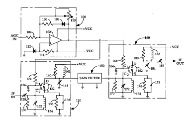
Figure 2 illustrates in further detail an exemplary embodiment of
the amplification circuit of Figure 1. Compensation circuit I00 receives an
AGC signal and in response thereto generates the appropriate
compensation. The resulting compensation signal is output from
compensation circuit 100 to both amplifier circuits I20 and 160.
Amplifier circuit 120 receives and amplifies an input IF signal at a
1 0 gain level determined by the compensation signal. The amplified IF
signal is then output to filter 150 where it is bandpass filtered and output
to amplifier circuit 160. Amplifier circuit 160 receives the amplified and
filtered IF signal where amplified at a gain level determined by the
compensation signal. The amplified IF signal is then output from
1 5 amplifier circuit 160 for further processing.
Compensation circuit 100 is comprised of an operational amplifier,
op amp 102, which has an inverting input coupled to receive the AGC
signal through input resistor I04. The inverting input is also coupled to
the output of op amp 102 through a nonlinear feedback circuit comprised
2 0 of series coupled resistor 106 and diode 108 which are coupled in parallel
with variable resistor 110. The noninverting input of op amp I02 is
provided with a reference or bias voltage across diode 112 that is provided
through resistor 114 from the supply voltage -VCC. Resistors I04, 106 and
114 are typically of the same resistance, e.g., 10 KS2 value, while variable
2 5 resistor 110 is capable or providing a much larger resistance value, e.g.
50
Kf2.
In the operation of compensation circuit 100, when the AGC voltage
is above the bias voltage appearing at the noninverting input of op amp
102, the parallel resistance combination of resistor 106 and variable resistor
3 0 I10, along with input resistor 104 (R106 I IR1I0 / 8104) set a first slope
gain
curve for operation of op amp 102. When the AGC voltage is below the
bias voltage, the value of variable resistor 110 along with input resistor 104
(RI10 / RI04) set a second, and different, gain curve for operation of op
amp 102. Furthermore diodes 108 and I14 are preferably of the same type
3 5 such that changes in temperature affecting diode 108, and thus the
WO 92/07424 2 0 9 413 3 p~/US91/077n~
8
feedback, similarly affect diode lI4 and the bias voltage. In the alternative,
diode lI4 may be replaced by a temperature sensitive element such as a
thermistor. It should be understood that the bias voltage appearing at the
noninverting input of op amp I02 may be established at many different
levels and by many different ways that are well known in the art.
The compensation signal generated by compensation circuit 100 is
output from op amp 102 to both of amplifier circuits 120 and 160.
Amplifier circuit 120 is typically comprised of dual gate FET amplifier I22
which has one gate (G1) coupled through resistor 124 to the output of op
1 0 amp 102 and through capacitor 126 to ground. The other gate (G2) of FET
122 receives the input IF signal through variable capacitor 128, and is
coupled to ground through the parallel combination of resistor 130,
variable capacitor 132 and inductor I34. The source (S) of FET 122 is also
coupled to ground through the parallel combination of resistor I36 and
1 5 capacitor 138. The drain (D) of FE'T 122 is coupled to the supply voltage
+VCC through the parallel combination of resistor I40 and inductor 142
while also being coupled to ground through variable capacitor 144. The
drain (D) of FE T 122 is coupled to the input of SAW filter 150.
The voltage at gate (Gi) as determined by the output of op amp 102
2 0 controls the level of gain of FET I22. The input IF signal is amplified at
the determined gain level by FE'T I22 with the output voltage appearing
across the input transducer (not shown) of SAW filter 150. The parallel
combination of resistor 140 and inductor 142 are of values selected such
that, in combination with the output impedance of FET 122 appearing at
2 5 the drain (D), the impedance of this circuit supplies the source impedance
seen by SAW filter 150.
It may be shown by using simple, tuned matching networks, the
total insertion loss (IL) of the complete SAW filter is approximately:
30 2GaGs 2
IL, (1)
(Ga + Gs)2
where: Ga is the real part of the acoustic admittance; and
3 5 Gs is the real part of the source and load admittances.
CA 02094133 1998-12-02
_. 9
Also, it may be shown that the triple transit response (TTR) of the
complete filter is defined by:
2 Ga GS ~ 2 ~ Ga2 ~ 2
TTR - . (2)
(Ga + Gs)2 (Ga + Gs)2
Using the relationships set forth by equations (1) and (2), one can compute
that for a triple transit response of 30 dB, relative to the main signal, an
1 0 insertion loss of 12 dB can be achieved.
Amplifier circuit 160 is constructed in a manner similar to that of
amplifier circuit 120. Amplifier circuit 160 is is comprised of dual gate FET
amplifier 162, preferably the same as FET 122, which has one gate (Gl)
coupled through resistor 164 to the output of op amp 102 and through
1 5 capacitor 166 to ground. The other gate (G2) of FET 162 is coupled to the
output of SAW filter 150 for receiving the filtered and amplified IF signal
output therefrom, and is coupled to ground through the parallel
combination of resistor 170, variable capacitor 172 and inductor 174. The
source (S) of FET 162 is also coupled to ground through the parallel
2 0 combination of resistor 176 and capacitor 178. The drain (D) of FET 162 is
coupled to the supply voltage +VCC through the parallel combination of
resistor 180 and inductor 182 while also being coupled to ground through
variable capacitor 184., The output of FET 162 is provided through variable
capacitor 186 also coupled to the drain (D) of FET 162.
2 S The voltage at gate (G1), as determined by the output of op amp 102,
again controls the level of gain of FET 162. The IF signal output from
SAW filter 150 is amplified at the determined gain level by FET 162 with
the output voltage appearing at the output of variable capacitor 186. The
parallel combination of resistor 170 and inductor 172 are of values selected
3 0 such that, in combination with the input impedance of FET 162 appearing
at the gate (G2), the impedance of this circuit provides the proper load for
the output impedance of SAW filter 150.
In should be noted that the output impedance of a FET is typically
greater than the input impedance. In amplifier circuit 120, resistor 140 is
3 5 used to set the output impedance of the circuit to match the input of SAW
..3~V0 92/07424 2 0 9 413 3 PCT/US91/077~.2
filter 150. In amplifier circuit 160, resistor 170 is used to set the input
impedance of the circuit to match the output impedance of SAW filter 150.
The value of resistor 170 is lower in value than resistor 140 since the input
impedance of the FET is greater than its output impedance. This
5 mismatch in amplifier selected resistor values provides compensation for
the difference in FET input and output impedance for impedance
matching to any circuit element. In the embodiment shown herein, the
resistors largely set the impedances with variations in FET impedances are
not critical. It is further envisioned that more gain could be realized using
1 0 transformer matching techniques.
Figure 3 illustrates in graphical form the gain characteristics of the
amplifier circuit without compensation of the AGC signal. The solid line
and the dashed line respectively represent the actual gain characteristic
curve and the desired gain characteristic curve. The circuit has straight
1 5 line rnntrol of gain in dB for gain values from about -40 dB to about 20
dB.
The uncompensated amplifier circuit thus provides an operational region
of 60 dB, where gain in dB is a linear function of the input voltage applied
to the gain control input of the amplifiers. In the region below -40 dB, the
actual gain departs quite radically from the desired straight line desired
2 0 gain curve. It is this region below -40 dB which the present invention
predominantly seeks to provide an improved correlation to the desired
gain characteristic curve.
Figure 4 illustrates in graphical form the gain characteristics of the
amplifier circuit with compensation of the AGC signal. The solid line and
2 5 the dashed line again respectively represent the actual gain
characteristic
curve and the desired linear gain characteristic curve. The circuit has
straight line control of gain in dB for gain values from about -75 dB to
about 10 dB. The compensated amplifier circuit thus provides an
operational region of operation of about 85 dB, where gain in dB is a linear
3 0 function of the input voltage applied to the gain control input of the
amplifiers. In the region below -75 dB, the actual gain is markedly loser
to the desired straight line gain curve than for the uncompensated circuit.
It is therefore readily be seen that by providing a compensated AGC signal
in the amplifier circuit of the present invention that an extended range of
CVO 92/07424 PCT/US91/07702
2094133
m
gain control in dB, which is a linear function of the input AGC signal, is
possible.
The previous description of the preferred embodiments is provided
to enable any person skilled in the art to make or use the present
invention. The various modifications to these embodiments will be
readily apparent to those skilled in the art, and the generic principles
defined herein may be applied to other embodiments without the use of
the inventive faculty. Thus, the present invention is not intended to be
limited to the embodiments shown herein but is to be accorded the widest
1 0 scope rnnsistent with the principles and novel features disclosed herein.
I CLAIM: