Note: Descriptions are shown in the official language in which they were submitted.
~ ~09~227
TITLE
VITAL RAILWAY SIGNAL LINR
BACKGROUND OF THE INVENTION
1. Field of the Invention.
The present invention relates generally to the
art of railway signaling. More particularly, the
invention relates to a vital apparatus and method for
transmitting railway signal information from an
electrical link input at a first terminal location to an
lo electrical link output at a second terminal location.
2. Description of the Prior Art.
In the control of railroad and rail-borne
transit vehicles, control signals are frequently passed
over significant distances. These control signals may,
for example, actuate switch turnouts to allow traffic
flow to branch from one track to another. Additionally,
the control signals may actuate wayside indicators to
display an appropriate aspect for the prevailing speed
conditions.
In order to prevent a system failure from
causing a problem, many railway signalling components are
designed to have "vital" characteristics. In the art,
the term "vital" signifies a component designed to give
the most restrictive condition in the event of a failure.
It is thus desirable to have signal links for passing
*
209~227
signal information between field locations be constructed
using vital design principles.
SUMMARY OF THE INVENTION
A vital railway signal link practicing the
present invention transmits information between an
electrical link input at a first terminal location and an
electrical link output at a second terminal location. In
response to a DC input signal applied to the electrical
link input, transmitting means at the first terminal
location emit a light signal modulated at a preselected
frequency. The light signal is transmitted to receiver
means at the second terminal location via an optical
conductor such as an optical fiber. A DC output signal
is then provided at the electrical link output. To
prevent stray ambient light from causing an errant output
signal at the electrical link output, discriminator means
are provided which assure essentially no output signal if
other than a light signal modulated at the preselected
frequency appears at the receiver means. Thus, the term
"discriminator" is used herein to signify means that are
adjusted to accept or reject signals of different
characteristics (such as amplitude or frequency).
In presently preferred embodiments, the light
signal is produced by application of the DC input signal
to a free running oscillator. A periodic electrical
2094227
-- 3 --
signal produced by the oscillator is applied to photo-
emission means, such as an infrared light emitting diode
driven by a Darlington emitter follower transistor
network. At the second terminal location, photo-
sensitive input means detect the periodic light signaland produce an analogous electrical signal. The
discriminator characteristics are preferably provided by
a relatively narrow bandpass filter which may be
constructed having a pair of resonant circuits coupled by
an electrical isolation coupler. The bandpass filter
receives the analogous electrical signal and produces a
filtered output signal. Signals of other frequencies are
blocked. Output means, which may comprise impedance
matching and amplification transistor networks feeding a
rectifier network, receive the filtered electrical signal
and produce the DC output signal.
Other presently preferred embodiments of the
invention are bidirectional, having a receiver and
transmitter at both terminal locations. Still other
embodiments utilize one or more repeaters to compensate
accrued line losses occurring in the conductor. Each
repeater may simply comprise a receiver having a DC
output tied to the DC input of a transmitter. Using such
repeaters, the effective operable length of the railway
signal link may be extended to virtually any desired
value.
2094227
- 4 -
BRIEF DESCRIPTION OF THE DRAWINGS
Figure 1 is a diagrammatic representation of a
vital railway signal link constructed in accordance with
the invention.
s Figure 2 is a schematic diagram of a presently
preferred transmitter for use with the railway signal
link of the invention.
Figure 3 is a schematic diagram of a presently
preferred receiver for use with the railway signal link
of the invention.
Figure 4 is a diagrammatic representation of a
bidirectional railway signal link of the invention.
Figure 5 is a diagrammatic representation of a
railway signal link of the invention utilizing an
interposing repeater to extend operable length.
DETAILED DESCRIPTION OF PRESENTLY PREFERRED EMBODIMENTS
In accordance with the invention, a vital link
may be provided to transmit railway signal information
from an electrical link input at a first terminal
location to an electrical link output at a second
terminal location. Unlike simple copper conductors used
in the prior art, the link utilizes an optical conductor
as the transmission medium. Thus, in addition to being
vital, the link is relatively immune to external
electromagnetic interference. The link is also generally
209~227
incapable of generating interference to any apparatus
operating in its vicinity.
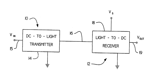
Figure 1 illustrates a presently preferred
railway signal link utilized to transmit signal
information from first terminal location 10 to second
terminal location 12. Specifically, DC-to-light
transmitter 14 receives a DC input signal VIN from input
15 and responsively emits a light signal onto optical
fiber 16. The light signal is then received by light-to-
DC receiver 18. Receiver 18, which is powered by asource voltage Vs, gives a DC output signal V0uT on link
electrical output 19.
As shown in Figure 2, transmitter 14 preferably
comprises an oscillator 22 electrically coupled to photo-
emission means 24. In presently preferred embodiments,oscillator 22 is a Colpitts type of oscillator, although
other oscillators may function adequately in this
application. At the core of oscillator 22 is NPN
transistor 26. The base of transistor 26 is biased using
a voltage dividing network comprising resistors 27 and
28. A capacitor 29 is provided to further stabilize bias
voltage. The periodic frequency of oscillator 22 is
preselected by choice of component values within a tank
circuit having an inductor 30 and capacitors 31 and 32.
The nodal junction 33 between capacitors 31 and 32 is
connected through resistor 34 to the emitter of
209~227
transistor 26. This provides a path for regenerative
feedback to sustain oscillation. The emitter of
transistor 26 is also connected to ground terminal 35
through bias resistor 36.
The periodic electrical output of oscillator 22
is fed via output line 37 to coupling capacitor 40.
Capacitor 40 serves to block any DC component in the
signal on line 37 so that an AC signal is applied to the
base of transistor 41. The emitter of transistor 41 is
lo connected to the base of transistor 42, thus forming a
common-emitter Darlington transistor network. The
emitter of transistor 42 is connected to the serial
combination of an infrared light emitting diode ("IR-
LED") 44 and current limiting resistor 45. The common-
emitter Darlington transistor network thus serves as abuffer amplifier between the higher output impedance of
oscillator 22 and the lower input impedance of IR-LED 44.
When the positive half-wave voltage at the emitter of
transistor 42 rises to a sufficient bias level, IR-LED 44
conducts and generates a pulse of light energy. A light
signal modulated at the preselected frequency is thus
produced on optical fiber 16, which is attached by
optical fiber connector 46.
Referring to Figure 3, receiver 18 generally
comprises an input section 50, a discriminator section
51, and an output section 52. Generally, input section
2094227
50 receives the light signal from optical fiber 16 (which
is connected via optical fiber connector 55) and produces
an analogous electrical signal periodic at the
preselected frequency. This is accomplished by first
applying the periodic light signal to the base of photo-
sensitive transistor 56. The emitter of transistor 56 is
connected to the base of transistor 57, thus forming a
photo-Darlington transistor network. The emitter of
transistor 57 is connected to ground terminal 60 through
resistor 61. To provide impedance matching between the
photo-Darlington transistor network and discriminator
section 51, an interposing emitter-follower transistor
network is provided. Specifically, the emitter of
transistor 57 is capacitively coupled through capacitor
62 to the base of NPN transistor 63. The base of
transistor 63 is biased by a voltage dividing network
comprising resistors 64 and 65. The collector of
transistor 63 is connected to supply terminal 66 through
resistor 67. A shunting capacitor 68, also connected to
the collector of transistor 63, essentially shorts any
undesirable harmonics appearing at this point. The
emitter of transistor 63, connected to ground terminal 60
through resistor 69, forms the output terminal for input
section 50.
Discriminator section 51 comprises circuitry
producing a filtered electrical signal upon receiving a
~ 209~227
periodic electrical signal at the preselected frequency.
Otherwise, section 51 produces essentially no signal at
its output. In presently preferred embodiments, section
51 comprises a narrow bandpass filter having a pair of
resonant circuits respectively tuned to the preselected
frequency and electromagnetically coupled but
galvanically isolated using transformer 72. The resonant
circuits are series LC circuits, respectively having
capacitors 73 and 74 and inductors 75 and 76. This
configuration insures, for example, that ambient light
which may be transmitted to receiver 18 if optical fiber
16 should break or become disconnected will not give an
errant output.
Further vital enhancement may be provided by
generally deriving the preferred inductance value LT f
the transformer windings according to the following
relationship: LT=LC/Q, where Lc is the inductance and Q
is the "quality factor" of the respectively connected of
inductors 75 or 76. The quality factor is derived from
the following equations:
(1) For a tuned circuit:
Q = f/B, where:
f is the tuned frequency, and
B is the desired bandwidth
209~227
g
(2~ For a coil:
Q = 2~fLC/Rc, where:
Rc is the coil resistance
As shown, the quality factor is a function of
frequency, desired bandwidth, inductance and coil
resistance. Thus, it becomes an application specific
variable. However, the quality factor of the resonant
circuits should generally be kept as high as practically
possible. According to the equation for LT above, this
will force the inductance and hence the quality factor of
the transformer windings to be relatively low with
respect to the associated resonant circuit. As such,
relatively small changes in transformer parameters will
"break" the link between the input and output of section
51. This is a desirable result in a vital
implementation.
For example, in an experimental prototype of
this embodiment, a preselected frequency of 1000 Hertz
was chosen. Inductors 75 and 76 were realized by
practical inductors having a coil resistance of
approximately 13 Ohms and inductance of approximately
86.9 MilliHenries(mH). As a result, a relatively high
quality factor of approximately forty-two (42) was
attained for the resonant circuits. Based on the
equation for LT, transformer 72 was implemented having
winding inductances of approximately 2.1 mH.
-lO- 2094227
Referring again to Figure 3, the filtered ou~uL of
section 51 is then fed to o~L~ section 52. For
impe~nce matching ~ul~o~es, this signal is first passed
to a common base transistor amplifier including NPN
transistor 77. The emitter of transistor 77 is connected
through bias resistor 78 which is used for input
impe~nce stabilization to ground terminal 60. The base
of transistor 77 is biased using a voltage divider
network comprising resistors 79 and 80. Capacitor 81
should have a value which essentially shunts resistor 80
at the preselected frequency. The collector of
transistor 77 is connected to supply terminal 66 through
resistor 82. The collector of transistor 77 is further
coupled through capacitor 83 to the base of NPN
transistor 84, which is biased by resistor 85.
Transistor 84 is here arranged as a common-emitter
amplifier. Thus, the emitter is connected directly to
ground terminal 60. A sufficient input voltage appearing
at the base of transistor 84 will cause a signal at the
collector of transistor 84. Resistor 86 serves as a
collector bias and load to transistor 84.
The output voltage appearing at the collector of
transistor 84 is then passed to a voltage doubling
rectifier network to produce DC ou~uL voltage V~T at the
link electrical output 19. Specifically, a coupling
capacitor 87 blocks any DC component in the output
voltage of transistor 84. The resulting AC signal is
VLS:jj
2094227
11
applied to the voltage doubling network which includes
diodes 88 and 89 and capacitor 90 to produce voltage
VOUT. This is a classical voltage doubling network known
in the art. It should be noted that because of the
circuit arrangement in the embodiment illustrated, the
polarity of V0uT is opposite that of VIN. This enhances
the vitality of the link since the expected polarity of a
signal at link electrical output 19 is also opposite of
Vs .
Figure 4 illustrates a bidirectional embodiment
of the railway signal link of the invention. This
configuration uses a transmitter and receiver pair at
each of locations 10 and 12 to communicate signal
information in both directions. Specifically, a
transmitter 14A at location 10 receives DC input signal
VlIN at input 15A. Signal VlIN is converted to a
periodic light signal and is conducted over optical fiber
16A to receiver 18A. Receiver 18A converts the light
signal to DC output signal VloUT on output l9A. In
addition, a DC input signal V2IN may be received on input
15B at location 12. Transmitter 14B converts signal V2IN
to a periodic light signal which is conducted over
optical fiber 16B to location 10. Receiver 18B receives
the light signal from optical fiber 16B and responsively
produces signal V2OuT on link output l9B. In this
embodiment, each directional transmitter-receiver pair
209~227
- 12 -
may be tuned to operate at different preselected
frequencies. Also, optical fibers 18A and 18B may be
constructed as a single, two fiber cable 93 or as part of
a larger bundle of fiber optic cable.
Although optical fiber has excellent photonic
conductivity characteristics, line losses can limit
effective length. Thus, as shown in Figure 5, the
railway signal link may be equipped to increase operable
length to virtually any desired value. Similar to other
embodiments, DC input signal VIN is received at link
electrical input 15C by transmitter 14C. Transmitter 14C
converts the electrical signal to a periodic light signal
which is applied to optical fiber 16C. Receiver 18C
produces DC output voltage VOUT at link electrical output
l9C. To compensate accrued losses, one or more
interposing repeaters 95 are positioned at points along
optical fiber 16C. Repeater unit 95 comprises a repeater
receiver 18D constructed as shown in Figure 3. Receiver
18D receives the light signal from a section of optical
fiber 16C and produces a DC repeater signal on electrical
conductor line 96. The DC repeater signal is applied to
the input of a transmitter 14D constructed as shown in
Figure 2. Transmitter 14D then outputs a compensated
light signal on a second section of optical fiber 16C.
2s It can thus be seen that a railway signal link
for transmitting information from a link electrical input
2094227
- 13 -
at a first terminal location to a link electrical output
at a second terminal location has been provided. The
link is constructed utilizing vital design principles so
that a failure of any component will generally reduce the
DC output signal to an unusable level. Discriminator
means are provided to protect against producing an output
signal due to ambient light or other unwanted input.
Certain preferred embodiments have been
described and shown herein. While the invention is
lo intended primarily to be used in railway signalling, it
may be useful in other environments. Thus, it is to be
understood that various other embodiments and
modifications can be made within the scope of the
following claims.