Note: Descriptions are shown in the official language in which they were submitted.
20g~983
:
SPECIFICATION
Title of the Invention
SUPERCONDUCTING INPUT INTERFACE
CIRCUIT FOR SUPERCONDUCTING CIRCUIT
Background of the Invention
Field of the invention
The present invention relates to a superconducting input interface
10 circuit for a superconducting circuit, and more specifically to a
superconducting interface circuit which transform a signal sent by an
ordinary electronic circuit to a suitable signal for a superconducting
circuit.
Description of related art
When a superconducting device or a superconducting integrated
circuit is adopted to an electronic equipment, it needs to be associated with
a conventional electronic circuit operating at an ordinary temperature.
Since it is still impossible for the superconducting device or the
2 0 superconducting integrated circuit to complete the entire electronic
equipment.
Owing to the real nature of superconducting phenomena, such as
problems of cooling etc., superconducting devices utilized in a
conventional electronic equipment are limited to a switching device and a
2 5 sensor device including a Josephson junction, a resister, a capacitor and an
inductor. Therefore, a complicated circuit still can not be composed of
only the superconducting devices alone. Moreover, the superconducting
2~9~3
circuit has a small voltage swing range less than millivolts. By this, a
weak signal of a few millivolts or a few microvolts are transferred
through the superconducting circuit.
In the prior art, in order to transmit a signal of several volts from
5 an ordinary electronic circuit to the superconducting circuit, the signal
should be converted to have a voltage swing of a few millivolts or a few
microvolts by a normal conducting interface circuit, and then this small
voltage swing signal is sent to the superconducting circuit cooled by liquid
nitrogen or liquid helium.
This small voltage swing signal sent to the superconducting circuit
from the interface circuit is easily affected and disturbed by external
electromagnetic waves. Therefore, multiplexing and coding of the small
voltage swing signal are restricted so as to decrease the possibility of
introducing an error from these processing. This restriction of the
multiplexing and coding of the small voltage swing signal leads to an
increase the number of signal lines. In addition, since the above
mentioned superconducting circuit has a small voltage/current gain, it has
insufficient drivability. In order to compensate for the drivability of the
superconducting circuit, the number of the signal lines further increases.
The stable transmission of the small voltage swing signal also
requires an complete electromagnetic shield around the signal lines. The
electromagnetic shield needs additional space.
The increase of the number of the signal lines and the attachment of
the electromagnetic shield bring difficulties for realizing a highly
2 5 integrated superconducting circuit.
2094983
Sllmm~ry of the Invention
Accordingly, it is an object of the present invention to provide an
input interface circuit for a superconducting circuit which has overcome
the above mentioned defect of the conventional one.
Another object of the present invention is to provide a
superconducting interface circuit which transform a signal sent by a
normal circuit to a suitable signal for a superconducting circuit.
The above and other objects of the present invention are achieved in
accordance with the present invention by a superconducting interface
circuit converting a signal sent from a normal conducting circuit into a
small voltage swing signal suitable for a superconducting circuit including
a superconducting field effect device (abbreviated as super-FET
hearinafter) having a superconducting channel of an extremely thin oxide
superconductor thin film, a superconducting source region and a
superconducting drain region of oxide superconductor thin films
positioned at the both ends of the superconducting channel, and a gate
electrode on the superconducting channel through a gate insulator, the
gate electrode being connected to a signal line which transmits a voltage
signal from the normal conducting circuit.
2 0 The superconducting interface circuit in accordance with the
present invention can directly receive a signal of several volts sent by an
ordinary electronic circuit, for example a CMOS circuit. Therefore, by
using the superconducting interface circuit in accordance with the present
invention, the signal transmission from the ordinary electronic circuit
section to the superconducting section becomes stable and is hard to be
affected by an environmental electromagnetic field. In addition,
multiplexing and coding of the signals become much easier.
2~94g83
By all of these, the number of signal lines between the ordinary
electronic circuit section and the superconducting section can be reduced
and an electromagnetic shield for the signal lines can be omitted so that a
high packing arrangement becomes possible.
The super-FET utilized in the superconducting interface circuit has
a superconducting channel of an extremely thin oxide superconductor.
Superconducting current flows through the superconducting channel is
controlled by a signal voltage of several volts applied to a gate electrode
arranged on the superconducting channel through a gate insulator. For
example, if the superconducting channel of an oxide superconductor has a
thickness of 5 nanometers, the gate can be closed by a voltage of 5 volts
and superconducting current is completely shut off. Therefore, a signal
voltage of 5 or 3.3 volts from a CMOS device can be directly sent to the
gate electrode of the super-FET and can directly drive the super-FET. In
addition, superconducting current of 1 0 mA can flow through the
superconducting channel having a width of 100 ~m.
This large current capability of the super-FET makes it possible
that plural superconducting circuit is connected to the superconducting
interface circuit through a superconducting bus or a magnetic coupling.
It is preferable that the superconducting channel, superconducting
source region and superconducting drain region of the above super-FET
are formed of for example YlBa2Cu3O7 ~ oxide superconductor material.
In this connection, these superconducting regions are preferably formed
of not only YlBa2Cu3O7 ~ oxide superconductor material but also a
2 5 high-TC (high critical temperature) oxide superconductor material,
particularly a high-TC copper-oxide type compound oxide superconductor
material, for example a Bi-Sr-Ca-Cu-O compound oxide superconductor
20~4~8~
material, and a Tl-Ba-Ca-Cu-O compound oxide superconductor material.
By using one of these oxide superconductor, a super-FET even operating
under liquid nitrogen cooling can be realized.
The above and other objects, features and advantages of the present
5 invention will be apparent from the following description of preferred
embodiments of the invention with reference to the accompanying
drawings.
Brief Description of the Drawings
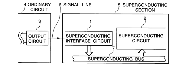
Figure 1 is a block diagram of an embodiment of the electronic
equipment including the superconducting interface circuit in accordance
with the present invention;
Figure 2 is a schematic wiring diagram of an embodiment of the
superconducting interface circuit in accordance with the present invention
1 5 used in the electronic equipment shown in Figure 1;
Figure 3 is a block diagram of another embodiment of the
electronic equipment including the superconducting interface circuit in
accordance with the present invention;
Figure 4 is a schematic wiring diagram of another embodiment of
20 the superconducting interface circuit in accordance with the present
invention used in the electronic equipment shown in Figure 3; and
Figure 5 is a schematic sectional view of a superconducting field
effect device (super-FET) utilized in the superconducting interface circuit
in accordance with the present invention.
20~4~83
.
Description of the Preferred embodiments
Referring to Figure 1, there is shown a diagram of an embodiment
of an electronic equipment including the superconducting interface circuit
in accordance with the present invention. The electric equipment includes
5 an ordinary semiconductor circuit 4 and a superconducting section 5
which are connected to each other by a signal line 6. The
superconducting section 5 includes a superconducting interface circuit 1 in
accordance with the present invention and a superconducting circuit 2, for
example a superconducting signal processor, utilizing an oxide
10 superconductor which are connected through a superconducting bus 7. As
explained hereinafter, the superconducting bus 7 is driven by the
superconducting interface circuit in accordance with the present
invention. The entire superconducting section 5 is cooled by liquid
nitrogen.
The ordinary circuit 4 includes an output circuit 3 utilizing a CMOS
semiconductor device, which are connected to the superconducting
interface circuit 1 by the signal line 6, precisely. A signal transmission
along the signal line 6 has an output voltage level of 5.0 volts or 3.3 volts,
which is produced by the CMOS semiconductor device of the output
2 0 circuit 3. This ordinary voltage level signal is difficult to be disturbed by
external electromagnetic fields. The signal is converted to a small voltage
swing signal which is suitable for the superconducting circuit 2 by the
superconducting interface circuit and is sent to the superconducting circuit
2 through the superconducting bus 7. Therefore, in the electronic
2 5 equipment including the superconducting interface circuit 1 in accordance
with the present invention, the small voltage swing signal is transmitted
only in the superconducting section 5. Since it is easy to form a magnetic
2~94~8~
.
shield which covers the entire superconducting section 5 and this magnetic
shield does not need so large space, stable signal transmission from the
ordinary circuit 4 to the superconducting section 5 and high density
integration becomes possible in the electronic equipment.
Figure 2 shows a wiring diagram of an embodiment of the
superconducting interface circuit which is used in the electronic
equipment shown in Figure 1. The superconducting interface circuit
includes a first super-FET l l which has a gate connected to the signal line
6, a source connected to the superconducting bus through a resister 13 and
a drain connected to the ground line 16, and a second super-FET 12
which has a drain and gate connected to the superconducting bus through
the resister 13 and source connected to a power line l5. As explained in
detail hereinafter, the super-FETs l l and 12 have a large superconducting
current capability and the flow of the superconducting current is
controlled by a signal voltage of several voltages applied to their gates.
Therefore, the signal transmitted along the signal line 6 of 5.0 volts or 3.3
volts can be converted to a small voltage swing signal suitable for the
superconducting circuit 2 by this superconducting interface circuit.
Figure 3 shows another embodiment of an electronic equipment
including the superconducting interface circuit in accordance with the
present invention. The electronic equipment includes an ordinary
semiconductor circuit 4 and a superconducting section 5 which are
connected to each other by a signal line 6 similarly to that of Figure 1.
The superconducting section 5 includes a superconducting interface circuit
2 5 1 in accordance with the present invention and a superconducting circuit 2
utilizing an oxide superconductor which are connected by a magnetic
coupling utilizing a solenoid 14. This is the only difference of this
9 8 3
electronic equipment from that of Figure 1. Therefore, more explanation
is abbreviated.
Figure 4 shows a wiring diagram of an embodiment of the
superconducting interface circuit which is used in the electronic
5 equipment shown in Figure 3. The superconducting interface circuit 1
has the same composition except that it does not include the resister 13
and is not connected to the superconducting bus. As explained above, the
superconducting interface circuit 1 is magnetically coupled to the
superconducting circuit 2 by the solenoid 14, which is positioned near the
1 0 super-FET 11.
Figure 5 shows a schematic sectional view of an embodiment of a
super-FET which is used in the superconducting interface circuit in
accordance with the present invention. The super-FET 20 includes a
substrate 25, a superconducting channel 21 of an oxide superconductor
15 thin fi]m having a thickness of on the order of 5 nanometers formed on
the substrate, a superconducting source region 22 and a superconducting
drain region 23 of an oxide superconductor thin film having a thickness
of 200 nanometers formed at the both ends of the superconducting
channel 21. The super-FET further includes a gate electrode 24 on the
2 0 superconducting channel 21 through a gate insulator 27. In the
super-FET, superconducting current flowing through the superconducting
channel 21 is controlled by a signal voltage of several volts applied to the
gate electrode 24.
The super-FET has large current capability and current driving
2 5 ability so that it can send superconducting signals to plural
superconducting circuits through a superconducting bus or magnetic
coupllng.
2~94g~
It is preferable that the superconducting channel, superconducting
source region and superconducting drain region of the above super-FET
are formed of for example YlBa2Cu307~ oxide superconductor material.
In this connection, these superconducting regions are preferably formed
5 of not only YlBa2Cu307 ~ oxide superconductor material but also a
high-TC (high critical temperature) oxide superconductor material,
particularly a high-TC copper-oxide type compound oxide superconductor
material, for example a Bi-Sr-Ca-Cu-O compound oxide superconductor
material, and a Tl-Ba-Ca-Cu-O compound oxide superconductor materiah
As mentioned above, superconducting current flowing through the
superconducting channel of the super-FET is controlled by a signal
voltage of several volts applied to the gate electrode~ Therefore, the
signal can be directly sent from a CMOS device to the gate electrode of
the super-FET~ By using the superconducting interface circuit in
15 accordance with the present invention, it becomes unnecessary to convert
a signal into a small voltage swing signal suitable for a superconducting
circuit before the signal is sent from a normal conducting circuit, so that
the signal sent from the normal conducting circuit has an ordinary level~
This makes it easy to send a multiplexed and coded slgnal from a normal
2 0 conducting circuit to a superconducting circuit~
The invention has thus been shown and described with reference to
the specific embodiments~ However, it should be noted that the present
invention is in no way limited to the details of the illustrated structures
but changes and modifications may be made within the scope of the
2 5 appended claims~