Note: Descriptions are shown in the official language in which they were submitted.
-
- 1 - 2C9~0~9
SPECIFICATION
OPTICAL MIRROR AND OPTICAL DEVICE USING THE SAME
Technical Field
This invention relates to an optical mirror and an optical
device using the same, where the mirror is incorporated with a
plurality of dielectric reflection multilayer film coatings each
of which has high reflectance to plural wavelengths or with a
combination of dielectric reflection multilayer film coatings and
metal reflection film coatings, and more particularly, to an
optical mirror suitable for second harmonic generation, optical
mixing, optical parametric generation and the like applying
nonlinear optical effects.
Background Art
A nonlinear optical device for converting an optical
frequency by applying nonlinear interaction, e.g., second
harmonic generation, of an optical wave in a nonlinear optical
material, in many cases, uses two concave reflection mirrors for
laser-resonating. One of these reflection mirrors is a total
reflection mirror (or a high reflection mirror) while the other
is a reflection mirror through which a portion of laser beam
transmits.
The high reflection mirror among them comprises, as shown
in, for example, Fig. 4, plural reflection multilayer films 2 and
3 consisting of a plurality of reflection films 2a, 2b, 3a, and
3b laminated on one surface of a transparent substrate 1, each of
which multilayer films 2 and 3 corresponds to each wavelength of
plural wavelengths of a light beam to selectively reflect one of
-
- 2 - 2~
said plurality of wavelengths, respectlvely. Each of the
reflectlon multllayer films 2 and 3 is formed by alternately
laminating usually different dielectric materials (e.g., S102
and T102), as shown hereln as the reflectlon fllms 2a and 2b
or 3a and 3b, at such a film thickness as belng capable of
providlng a maxlmum reflectance at each speclfic wavelength.
However, in the conventional optlcal mlrror for use
ln a plurallty of wavelengths, as shown in Flg. 4, there ls
consldered only a reflection amplitude, so that a phase
matching condltlon requlred for nonllnear optical materlals ls
not satisfied. As a result, when the second harmonlc
generatlon, the optical mlxlng or the like is performed using
the nonlinear optlcal materlal, there occurs a disadvantage of
decreasing efflciency due to a phase shift between an excltlng
light beam and a newly generated light beam when these light
beams are reflected by a mirror.
SUMMARY OF THE INVENTION
An ob~ect of the present invention is to provide an
optical mirror and an optical device using the same in which
the mlrror ls capable of reflectlng a light beam having a
plurality of wavelengths with the phase matchlng condltion
requlred for nonlinear optlcal materlals belng satlsfled, so
that no decrease in efflciency due to the phase shift
generates even if the harmonic generation, the optical mlxing
or the like is performed, thereby being capable of improving
conversion efflclency.
72689-56
- 3 - 2 ~
In order to achleve the above mentioned ob~ect, the
present inventlon resldes ln an optlcal mlrror comprlsing a
plurallty of reflectlon films formed on an edge surface of a
transparent substrate each of whlch films corresponds to one
of a plurallty of wavelengths of a llght beam havlng said
plurality of wavelengths to reflect selectively one of sald
plurality of wavelengths, characterized by comprlslng
a phase dlfference ad~ustlng layer formed between
two reflection films reflectlng light beams havlng dlfferent
wavelengths, said ad~ustlng layer adiusting lnterrelatlon
between a phase of the llght beam reflected by one of the
reflectlon fllms and a phase of the llght beam reflected by
the other of the reflectlon fllms.
The present lnventlon may apply the followlng
embodlments.
(1) The plural wavelengths constltutlng the llght beam
are ln a relatlon of a multlple of an lntegral number or ln
relatlon of a reclprocal of an lntegral number wlth each
other.
(2) Sald phase dlfference ad~ustlng layer ls made of the
same materlal as any one of sald reflectlon fllms.
(3) Sald phase difference adjusting layer consists of an
alr gap.
(4) Sald phase dlfference adiustlng layer is formed
between ad~acent two reflectlon multllayer fllms.
(5) Sald reflectlon fllms each are lamlnated as two
layers. Of course, more layers may be applied.
72689-56
- 4 ~
(6) Sald reflection fllms conslst of multllayer fllms.
(7) One of sald reflectlon fllms ls a reflectlon fllm
such as a metal fllm (e.g., alumlnum) whlch ls non-selectlve
to wavelengths.
(8) Sald reflectlon fllms conslst of multllayer fllms,
and sald phase dlfference ad~ustlng layer ls not formed
between a flrst reflectlon multllayer fllm for reflectlng a
llght beam havlng a certaln wavelength and a second reflectlon
multllayer fllm for reflectlng a llght beam havlng a
wavelength dlfferent from the above wavelength but ls formed
between the multllayer fllms of the flrst reflectlon
multllayer fllm or between the multllayer fllms of the second
reflectlon multllayer fllm.
(9) The transparent substrate ls made of glass, a
nonllnear optlcal crystal, a metal or the llke. All posslble
comblnatlons of (1) to (9) may be also applled.
An optlcal mlrror accordlng to the present lnventlon
can be applled to varlous optlcal devlces such as a second
harmonlc generatlng devlce, a multl-wavelengths mixlng devlce,
a sum frequency generatlng devlce, a dlfference frequency
generatlng devlce or a parametrlc osclllatlng devlce.
Prlnclples of the present lnventlon wlll be
descrlbed wlth reference to Flgs. 1 and 6.
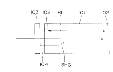
As shown ln Flg. 1, when the second harmonlc
generatlon of a llght beam ls performed uslng, for example,
KNbO3, reflectlon fllms 102, for example, 860 nmHR are at
flrst formed on both end surfaces of KNbO3 101, respectlvely,
72689-56
~ 2 ~ ~ 5 ~ ~ ~
- 4a -
to trap a fundamental wave of 860 nm between the reflectlon
films for 860 nmHR. Thls results ln generatlon of a second
harmonlc (SHG) of 430 nm from the end surfaces. The output
thereof is indlcated by
72689-56
} r,
; ~,
-- 5
a 11ne S (~ -O -O ) in Fig. 6.
Subsequently, a reflection film 103 for 430 nmHR is
laminated on one of the reflection films for 860 nmHR. As a
result, the second harmonic of 430 nm is reflected by the
reflection film for 430 nmHR and emerges from the other end
surface. The output of this case is indicated by a line W
(O -O -O ) in Fig. 6. It is because the phase is reversed that
the output becomes zero at a wavelength of 1.3. In this event,
no gap is especially formed between the left-hand reflection film
102 for 860 nmHR and the reflection film 103 for 430 nmHR in Fig.
1.
To match the phase difference between the light beam of
430 nm and that of 860 nm, a phase difference ad~usting layer 104
is formed between the reflection film 102 for 860 nmHR and the
reflection film 103 for 430 nmHR. The resulting output is as
indicated by a line C (~ -~ -~ ) in Fig. 6.
The film thickness of the phase difference ad~usting
layer, i.e., a distance between the reflection film for 860 nmHR
and the reflecting film for 430 nmHR, which is equal to 4A /5 (A
= 430 nm) in this example, is determined depending on the phase
difference for each case.
A preferred embodiment of the present invention will be
described below with reference to the drawing.
An optical mirror according to the present invention will
be described with reference to the drawing in which, Fig. 2 shows
an optical mirror according to an embodiment of the present
invention when applied to a light beam having two different
CA 0209~019 1999-01-14
wavelengths. The optical mirror comprises a first reflection
multilayer film 2 for reflecting selectively one wavelength of
the two wavelengths of said light beam, formed on one surface
of a transparent substrate 1 such as a concave mirror, a
second reflection multilayer film 3 adjacent to the reflection
multilayer film 2 for reflecting selectively the other
wavelength, and a layer 4 positioned therebetween for
adjusting phase difference between the light beams reflected
by said two reflection multilayer films 2 and 3.
The first reflection multilayer film 2 comprises a
laminate of two reflection films 2a and 2b each reflecting
selectively one wavelength, said laminate being prepared by
alternately laminating each reflection film. The second
reflection multilayer film 3 comprises a laminate of two
reflection films 3a and 3b each reflecting selectively the
other wavelength, said laminate being prepared by alternately
laminating each reflection film. The method itself for
forming the first reflection multilayer film 2 or the second
reflection multilayer film 3 may be the same as the
conventional method, which can be formed typically by
selecting two of the dielectric materials such as SiO2 and
Tio2, depending on the selected wavelength to laminate
alternately the dielectric materials at such a film thickness
providing a maximum reflectance at each specific wavelength as
being capable of (generally a film thickness corresponding to
72689-56
CA 02095019 1999-01-14
- 6a -
1/2 or 1/4 wavelength) using techniques such as deposition or
sputtering.
The thickness of the reflection multilayer film 2 or
3 is
72689-56
~ 2~50 ~9
7 72689-56
generally about 2 ~ 4 ~m, though lt slgnlflcantly varles dependlng
on the thlckness or the number of layers of the reflectlon fllms
2a, 2b or 3a, 3b.
In addltion, ln the present lnventlon, the layer 4 ls
formed between ad~acent two reflectlon multllayer fllms 2 and 3,
whlch layer ad~usts the phase dlfference between the llght beams
reflected by the refectlon multllayer fllms. The layer 4 ls a
layer for reflectlng the llght beams havlng a plurallty of
wavelengths at a speclflc phase dlfference by means of ad~ustlng
the lnterrelatlon, especlally the phase dlfference, between the
llght beams reflected by sald two reflectlon multllayer fllms ln
order to prevent a decrease ln efflclency due to the phase
relatlon between the llght beams of wavelengths reflected, and ls
made of the same dielectrlc materlal such as SlO2 or TlO2 as the
materlal of the reflectlon fllm and preferably the same materlal
as the reflectlon materlal of one of the two reflectlon fllms.
The phase dlfference ad~ustlng layer 4 may preferably be
formed between the two reflectlon multllayer fllms 2 and 3, though
lt may be formed between any ad~acent two reflectlon fllms 2a and
2b or 3a and 3b composed of the reflectlon multllayer fllm 2 or 3
of the ad~acent two reflectlon multllayer fllms 2 and 3.
As a method for preparlng the phase dlfference ad~ustlng
layer 4, a method such as deposltlon or sputterlng ls generally
applled. The thlckness of the phase dlfference ad~ustlng layer 4
ls generally about 0.2 ~ 1 ~m lncrease of correspondlng to 1/2
wavelength or about 0.05 ~ O.S ~m ln case of correspondlng to 1/4
wavelength, though lt may be varled dependlng on the phase
difference.
8 72689-56
Llght beams applled to the optlcal mirror accordlng to
the present lnventlon may be those havlng a plurallty of
wavelengths.
Whlle the optlcal mlrror accordlng to the present
inventlon has thus been described ln con~unction wlth the example
of appllcatlon to the llght beam havlng two wavelengths, lt ls
apparent that the present lnventlon can be applled to a llght beam
havlng three or more wavelengths by means of provldlng all of the
reflectlon multllayer films which has hlgh reflectance corres-
ponding to each wavelength as well as providlng all of the abovementloned phase dlfference ad~ustlng layer formed between the
ad~acent two reflectlon multllayer fllms or between any ad~acent
two reflectlon fllms of elther one of the reflectlon multllayer
fllms among these reflectlon multllayer fllms. Further, lt ls
apparent that the reflectlon fllms consistuting each of the
multllayer reflectlon fllms may be three or more klnds, though the
reflectlon fllms are two klnds ln sald example.
Next, an embodlment of the optlcal mlrror accordlng to
the present lnventlon applled to an optlcal devlce capable of
uslng for second harmonlc generatlon ls shown ln Flg. 3.
In Flg. 3, 11 represents a laser dlode, 12 represents a
Faraday lsolator, 17 represents a colllmator lens, 13 represents a
condenser lens, 14 represents a two-wavelengths hlgh reflectlon
concave mlrror (an optlcal mlrror), 15 represents a slngle
wavelength hlgh reflectlon concave mlrror and 16 represents a
nonllnear optlcal monocrystal. The optlcal mlrror accordlng to
the present lnventlon ls set and used at the posltlon 14.
Actlon of the optical mlrror ls descrlbed ln con~unctlon
9 72689-56
wlth an example shown ln Flg. 2. In one embodlment, one wave-
length of a llght beam havlng two wavelengths lntroduced from the
slde of the transparent substrate 1 ls reflected by the reflectlon
multllayer fllm 2, durlng passlng therethrough, whlch ls composed
of lamlnated two dlfferent reflectlon fllms 2a and 2b. The other
wavelength transmlts through the reflectlon multllayer fllm 2 and
the phase dlfference ad~ustlng layer 4 wlthout belng substantlally
reflected, whlch ls then reflected by the reflectlon multllayer
fllm 3, durlng passlng therethrou~h, whlch ls comprlsed of
lamlnated two dlfferent reflectlon fllms 3a and 3b. In another
embodlment, one wavelength of a light beam havlng two wavelengths
lntroduced from the opposlte slde of the transparent substrate 1
ls reflected by the reflectlon multllayer fllm 3 comprlsed of sald
reflectlon fllms 3a and 3b durlng passlng therethrough. The other
wavelength transmlts through the reflectlon multllayer fllm 3 and
the phase dlfference ad~ustlng fllm 4 wlthout belng substantlally
reflected, whlch ls then reflected by the reflectlon multllayer
fllm 2 composed of sald reflectlon fllms 2a and 2b durlng passlng
therethrough. In elther case, the phase dlfference between the
llght beams reflected by both reflectlon multllayer fllms 2 and 3
ls ad~usted by the phase dlfference ad~ustlng layer 4 formed
between these multllayer fllms. Accordlngly, sald llght beam
havlng a plurallty of wavelengths ls reflected due to the speclflc
phase dlfference. Thls results ln preventlon of an efflclency
decrease due to the phase relatlon.
In addltlon, when such an optlcal mlrror ls set at 14 of
an optlcal devlce as shown ln Flg. 3 to perform the second
harmonlc generatlon, the optlcal mlrror reflects the llght beam
72689-56
havlng a plurallty of wavelengths whlle satlsfylng the phase
matching condltlon requlred for the nonllnear optlcal effect,
thereby lmprovlng converslon efficiency.
Brlef Descrlptlon of the Drawlnq
Fig. 1 is a view showlng the actlon prlnclple of an
optlcal mlrror accordlng to the present lnventlon;
Flg. 2 ls a partlally cutaway sectlonal vlew showing an
optlcal mirror accordlng to an embodlment of the present
lnventlon;
Flg. 3 ls a schematlc slde vlew of an optlcal devlce
uslng an optlcal mlrror accordlng to the present lnventlon7
Flg. 4 ls a partlally cutaway sectlonal vlew showlng the
conventlonal optlcal mlrror made ln comparatlve Example;
Flg. 5 ls a partlally cutaway sectlonal vlew showlng a
referentlal optlcal mlrror made ln Reference Example; and
Flg. 6 shows hlgh-frequency curves measured uslng an
optlcal devlce accordlng to Example 2 ln whlch optlcal mlrrors
made ln Example 1 and Comparatlve Examples 1 and 2 are set.
Best Mode For CarrYlnq Out The Inventlon
Practlcal examples are descrlbed where the above
mentloned optlcal mlrror ls applled.
cExample 1>
As shown ln Flg. 2, a flrst reflectlon multllayer fllm 2
that exhlblts a hlgh reflectance at 430 nm was formed on a
transparent substrate 1, whlch ls made of a standard glass of BK7
glass produced by Slgma Optlcal Devlce Inc., by alternately
lamlnating a reflectlon fllm 2a (~2n=0.13 um ln thlckness)
11 72689-56
conslstlng of SlO2 thln fllms and a reflectlon fllm 2b (~./2n=
0.10 ~m in thlckness) conslstlng of TlO2 thln fllms uslng
deposltion at such a fllm thlckness as belng capable of provldlng
a maxlmum reflectance at a wavelength of 430 nm to produce twenty-
nlne layers (fourteen cycles plus one layer). SlO2 was then
lamlnated thereon to form a phase dlfference ad~ustlng layer 4
(0.21 ~m ln thlckness) accordlng to deposltlon at a thlckness
correspondlng to substantlally 4 ~/5 at a wavelength of 430 nm 4
~/5 ~ ~=430nm) - thlcker ln optlcal thickness when measured at 430
nm than those of reflectlon fllms 3a conslstlng of SlO2 thln fllms
at the thlrty flrst layer and later to be formed thereafter (after
formlng the phase dlfference ad~ustlng layer at the thlrtleth
layer). A second reflectlon multllayer fllm 3 that exhlblts a
hlgh reflectance at 860 nm was formed thereon by alternately
lamlnatlng reflectlon fllms 3a (0.21 ~m ln thlckness) conslstlng
of TlO2 thln and reflectlon fllms 3b (0.26 ~m ln thlckness)
conslstlng of SlO2 thln fllms uslng deposltlon at such a fllm
thlckness as belng capable of provldlng a maxlmum reflectance at a
wavelength of 860 nm to produce twelve layers (6 cycles). Thus, a
two-wavelengths hlgh reflectlon optlcal mlrror (herelnafter
referred to as C-coat mlrror) was made wlth the forty-two layers
ln total.
<Comparatlve Example 1>
An optlcal mlrror (herelnafter referred to as W-coat
mlrror) for comparlson as shown ln Flg. 4 was made ln the same
manner as ln Example 1 except that the phase dlfference ad~ustlng
layer was not formed.
cComparatlve Example 2
'~ -
lla 72689-56
An optlcal mlrror (herelnafter referred to as S-coat
mlrror) for comparlson as shown ln Flg. 5 was made by alternately
lamlnatlng, on the transparent substrate l used in Example 1,
reflectlon fllms 3a (0.21 ~m ln thlckness) conslstlng of TlO2 thln
fllms and reflectlon fllms 3b (0.26 ~m ln thlckness) conslstlng of
SlO2 thln fllms by means of deposltlon at such a fllm thlckness as
belng capable of provldlng a maxlmum reflectance at a wavelength
of 860 nm to produce 12 layers (slx cycles).
cExample 2~
As shown ln Flg. 2, a flrst reflectlon multllayer fllm 2
that exhlblts a hlgh reflectance at 430 nm was formed on a
transparent substrate 1, whlch ls made of a standard glass of BK7
glass produced by Slgma Optlcal Devlce Inc., by alternately
lamlnatlng a reflectlon fllm 2a ( ~/4n=about 0.07 um ln thlckness)
conslstlng of S102 thln fllms and a reflectlon fllm 2b (~
/4n-about 0.05 ~m ln thlckness) conslstlng of TlO2 thln fllms
uslng deposltlon at such a fllm thlckness as belng capable of
provldlng a maxlmum reflectance at a wavelength of 430 nm to
produce twenty-nlne layers (fourteen cycles and one layer). SlO2
was then lamlnated thereon to form a phase dlfference ad~ustlng
layer 4 (0.24 ~m ln thlckness) correspondlng to substantlally 4
/5 at a wavelength of 430 nm) accordlng to deposltlon. A second
reflectlon multllayer fllm 3 that exhlblts a hlgh reflectance at
860 nm was formed thereon by alternately lamlnatlng reflection
fllms 3a (about 0.11 ym ln thlckness) conslstlng of TlO2 thln
fllms and reflectlon fllms 3b (about 0.15 ~m ln thlckness)
conslstlng of SlO2 thln fllms uslng deposltlon at such a fllm
thlckness as belng capable of provldlng a maxlmum reflectance at a
ll~ 72689-56
wavelength of 860 nm to produce twelve layers (slx cycles). Thus,
a two-wavelengths high reflectlon optlcal mlrror (herelnafter
referred to a C-coat mlrror) was made wlth the forty-two layers ln
total.
<Comparatlve Example 3~
An optlcal mlrror (herelnafter referred to as W-coat
mlrror) for comparlson as shown ln Flg. 4 was made ln the same
manner as ln Example 2 except that the phase dlfference ad~ustlng
layer was not formed.
<Comparatlve Example 4>
An optlcal mlrror (herelnafter referred to as S-coat
mlrror) for comparlson as shown ln Flg. 5 was made by alternately
lamlnatlng, on the transparent substrate 1 used ln Example 2,
reflectlon fllms 3a (about O.ll ym ln the thlckness) conslstlng of
T102 thln fllms and reflectlon fllms 3b (about 0.15 ~m ln
thickness) conslstlng of S102 thln fllms by means of deposltlon at
such a fllm thlckness as belng capable of provldlng a maxlmum
reflectance at a wavelength of 860 nm to produce twelve layers
(slx cycles).
Then, the respectlve C-coat mlrror ln Examples 1 and 2,
the respectlve W-coat mlrror ln Comparatlve Examples 1 and 3 and
the respectlve S-coat mirror ln Comparative Examples 2 and 4
2 ~ c
- 12
as mentioned above were alternately applied as the high
reflecting concave mirror 14 to the device shown in Fig. 3 to
measure second harmonic outputs.
Specifications for the device in Fig. 3 are as follows:
Laser diode 11:
Laser diode SLD7033101 produced by SANYO Co.
(The oscillation wavelength was
set at around 862 nm)
Faraday isolator 12:
Faraday ~solator ISO-7885 produced by New Port
Co .
Condenser lens 13:
Convex lens having a 62.9 mm focal length
prepared by applying low-reflective coating on a standard glass
of BK7 glass
Single wavelength high reflection concave mirror 15:
One having 99.95 % of reflectance at 860 nm with
a substance made of a standard glass of BK7 glass
Nonlinear optical monocrystal 16:
One prepared by optically polishing the a-surface
of a KNbO3 monocrystal having 6 mm length before applying low-
reflecting coating. The nonlinear optical monocrystal 16 was
held at about 31 C by ad~usting the temperature thereof using a
Peltier element.
Collimator lens 17: FL-40B convex lens manufactured by
New Port Co.
- 13
Distance between the mirrors 14 and 15: about 13 mm
In the optical device as above-mentioned, the harmonic
outputs were measured, at a wavelength to whlch the fundamental
wave of the resonator resonates, by means of varying the tempera-
ture of the nonlinear optical monocrystal 16 by O.l C, thereby
inducing an electric current in the laser diode.
The results are shown in Fig. 6 (in the figure, C is for
C-coat mirror, W is for W-coat mirror and S is for S-coat
mirror). The data obtained by changing the temperature of said
monocrystal 9 were converted to the wavelengths based on 0.3nm =
I ~ C .
As apparent from the results, C-coat mirror according to
the present invention provides the harmonic output of about
double as compared wlth W-coat mirror and S-coat mirror.
The present Example is an example of the second harmonic
generation using KNbO3 monocrystal, and when the optical mirror
of the present inventlon is used, an optical device such as a
highly effective nonlinear optical element can be manufactured
because high reflection is obtalned while satisfying the phase
malc~in~ condltlon rc(llllrc(l for cntlrc nonllncar optlcal crf'ccts
such as multiple wavelengths mixing, sum frequency generation,
difference frequency generation and parametric oscillation.
Industrial Applicability
According to the present invention it is possible to
provide an optical mirror and an optical device using the same in
which the mirror is capable of reflecting a light beam having a
plurality of wavelengths with the phase matching condition
14 72689-56
requlred for nonllnear optlcal materlals belng satlsfled, so that
a decrease ln efflclency due to the phase dlfference does not
generate even lf second harmonlc generatlon, optlcal mlxlng or
optlcal parametrlc osclllatlon are performed, thereby belng
capable of lmprovlng converslon efflclency.