Note: Descriptions are shown in the official language in which they were submitted.
W092/08226 ~ O 9 5~ 3~ PCT/US91/07822
UNSHIELDED HORIZONTAL MAGNETORESISTIVE HEAD
AND METHOD OF FABRICATING SAME
Field of the Invention
The present invention relates to an
unshielded horizontal magnetoresistive head which
may be utilized for magnetic sensing and reading.
Further, the present invention relates to such
heads which have cost and fabrication advantages
over current heads, and the method of fabricating
such heads. More particularly, the heads of the
present invention, may be utilized in a bill
validator to sense the magnetic properties
inherent in paper currency such as U.S. currency,
or to many other applications involving magnetic
sensing or reading which will be readily apparent
to those skilled in the pertinent art in view of
the following disclosure.
Background of the Invention
A magnetoresistive head is a sensing or
reading head which utilizes magnetoresistive
elements to sense or read magnetic information
inherent in a magnetic medium. A magnetoresistive
element is one whose electrical resistance varies
with varying incident magnetic fields.
Many prior art magnetic heads, for a
great many applications including coin sensing,
determining the contents of a coin tube, currency
and bill validation, and determination of the
denomination of ~I~.per currency or other forms of
scrip, are of the inductive type which require a
rapidly changing magnetic field in order for
magnetic information to be detected and recorded.
Magnetoresistive heads, on the other hand, are
capable of detecting and reading information
inherent in a slowly moving magnetic field. Prior
W092/08226 ~ O 9 5 ~ 3 5 PCT/US91/07822
to fabricate and consequently relatively
expensive, as further discussed below.
The orientation of a sensing element of a
magnetoresistive head may be either vertical or
horizontal in relation to the magnetic medium
which is being read. In the vertical orientation,
described in R.S. Indeck, J.H. Judy, and S.
Iwaski, "A Magnetoresistive Gradiometer," IEEE
Trans. Magn. 24, 2617 (1988), the magnetoresistive
head is situated on the magnetic medium in a
vertical or standing up position which places the
bottom edge of the head either in contact with or
closely adjacent to or near, the magnetic medium
which it is desired to read from.
A number of dual-element vertical
magnetoresistive sensors have been described in
the prior art literature for use with high
performance reading. In general, these vertical
structures have been comprised of two parallel
magnetoresistive elements or sensors placed in
close proximity to each other and standing
perpendicular to the plane of the magnetic medium
to be read. The advantages claimed for such
structures include good common noise rejection, a
broader range of linear performance (and
consequently, a reduction of second-harmonic
distortion), and a larger signal per unit width
than with single sensor heads.
Vertical magnetoresistive heads are
fabricated on a wafer, and then a strip cont~;njng
a number of these heads arranged in a row is cut
from the wafer. This cutting or separating
process creates burrs or rough edges on the
separated edges. The edge of this strip which
contacts the magnetic medium must then be
polished. This polishing step is critical because
it determines sensor height. As tolerance is
W 092/08226 Z ~ 9 5 ~ 3 5 PC~r/US91/07822
3-
typically very tight, the process is an expensive
one. The resulting polished strip is then diced
to separate the individual heads.
Fabrication of horizontal
magnetoresistive heads according to the present
invention is much simpler than the above described
vertical head fabrication method. In the present
invention, once the wafer containing the head has
been diced, it is the faces of the diced head
elements, and not their side edges, that are to be
used to either make contact with, or be placed
closely adjacent to, the magnetic medium to be
read. Hence, the present invention dispenses with
the costly and time consuming polishing process.
While horizontal magnetoresistive heads
are described in the prior art, such as by D.W.
Chapman, D.E. Heim and M.L. William, "A New,
Horizontal MR Head Structure," IEEE Trans. Magn.
25, 3689(1989) and D.W. Chapman, "A new approach
to making thin film head-slider devices," IEEE
Trans., Magn. 25,3686 (1989), these horizontal
magnetoresistive heads employed a shield and the
fabrication process employed to make them is
premised around the inclusion of this shield. The
present invention dispenses with such a shield and
provides a horizontal magnetoresistive reading
head which is unshielded. As a result, a simpler
and less expensive fabrication process is employed
to make unshielded horizontal heads according to
the present invention. These heads have
sufficient resolution to be highly desirable for
use in a host of applications not previously
recognized as appropriate fo~ more expensive
heads, and as a replacement for more expensive
heads presently utilized in certain applications.
W092/08226 2 ~ 9 5 ~ PCT/US91/07822
Summary of the Invention
It is an object of the present invention
to provide a horizontal, unshielded
magnetoresistive reading head for use in magnetic
sensing and reading devices and in other related
devices to perform analysis or verification of the
magnetic properties of certain magnetic media.
This invention may find application in bill
validators and the like where magnetic
verification means are presently employed.
A new variety of dual magnetoresistive
head is described in which the two
magnetoresistive elements or sensors are situated
in a common plane, either in contact with or
adjacent to the magnetic medium to be read, in a
horizontal configuration. Unlike prior art
horizontal heads, the present horizontal head is
unshielded.
Another object of the present invention
is to provide a simplified design and fabrication
process for magnetoresistive heads so that less
expensive and more efficient fabrication
procedures result.
The structure and method of use and
fabrication of the present invention will be
apparent to those skilled in the art from a review
of the Detailed Description in conjunction with
the drawings. Likewise, other objects of the
present invention will be readily apparent to
those skilled in the art.
W092/08226 ~ ~9 ~ 35 PCT/US91/07822
_5_
Description Of The Drawings
Fig. 1 depicts an unshielded horizontal
magnetoresistive head according to the present
invention;
Fig. 2 illustrates a prior art shielded
horizontal magnetoresistive head;
Fig. 3 is an illustration of a
magnetoresistive response curve for a strip of
magnetoresistive material before it is biased in
the transverse direction;
Fig. 4 is a magnetoresistive response
curve for a given strip of magnetoresistive
material after it has been biased in the
transverse direction;
Fig. 5 is a graphical representation of
an output signal from the unshielded horizontal
magnetoresistive head of Fig. l;
Fig. 6 is illustrative of the signals
produced by each magnetoresistive strip of the
magnetoresistive head of Fig. 1 as a magnetic
transition is moved across the magnetoresistive
head; and
Figs. 7 and 8 are illustrative of the
utilization of the magnetoresistive head of Fig. 1
to detect magnetic transitions in currency in a
currency validator.
Detailed Description
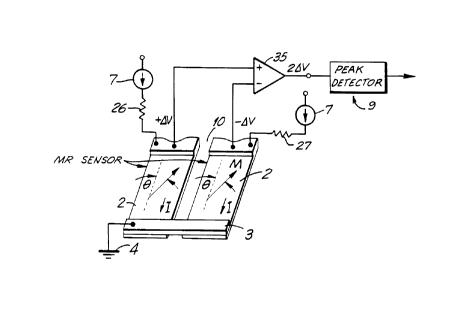
Referring to Fig. 1, a simplified
~ structural depiction of an unshielded horizontal
magnetoresistive head 1 according to the present
invention is shown. Two ma~netoresistive strips 2
lie parallel to one another in the same horizontal
plane, separated by a gap 10. The gap 10 may be
filled with air or any other type of dielectric
material, which is defined as an electrical
insulator capable of sustaining an electrical or
W092/08226 ~9 ~O ~ PCT/US91/07822
magnetic field with a minimum dissipation in
power. The magnetoresistive strips 2 are
connected at one end by a cross member element 3.
Cross member element 3 is an electrical conductor
and serves to structurally connect the
magnetoresistive strips 2, as well as, to
electrically connect them to a common electrical
point 4 which is typically system y OU~I~. The
ungrounded ends of each of the magnetoresistive
strips 2 are connected through equal valued
resistors 26 and 27 to a pair of constant current
supplies 7. As a result, the ungrounded ends of
each of the magnetoresistive strips 2 are also
connected to the inputs of a differential voltage
sensing device 35. Identical currents (I) flow
from the constant current supplies 7 through the
resistors 26 and 27, and then through each of the
magnetoresistive strips 2 to ground. A peak
detector circuit 9 is connected to the output of
the differential voltage sensing circuit 35.
The strips 2 should be as thin as
possible within practical design constraints so as
to maximize the voltage change developed across
each strip for a given magnetic transition or
signal to be sensed thus achieving a higher degree
of resolution. The size of the gap lO is
governed by the application to which the
magnetoresistive head is employed. To obtain
accurate results, the size of gap lO should be
such that no more than one magnetic transition
appears within the gap lO at any given instance in
the sensing or reading process. For applications
requiring a higher resolution, or where closely
spaced magnetic transitions are found, a small gap
size is necess~ry. In lower resolution
applications, where the magnetic transitions are
spaced farther apart, the size of the gap may be
W O 92/08226 ~ O 9 5 ~ 35 P(~r/US91/07822
larger so long as multiple transitions do not
occur within the gap at any given instance in
time.
Magnetoresistive elements, by their
nature, experience a change in electrical
resistivity or resistance as1a function of the
orientation of the magnetic~dipole moments that
occur in the material, when a magnetic field is
applied. Unlike inductive heads, magnetoresistive
elements may operate to sense a slowly changing
magnetic field.
Referring once again to Fig. 1, the
structure of the present invention consists of the
two magnetoresistive strips 2 separated by the gap
10. The strips 2 have substantially the same
electrical characteristics and substantially the
same current (I) flowing in them. As a result, in
the absence of a magnetic field, the voltage drop
across each of the strips is substantially the
same and the output of the differential voltage
amplifier 35 is essentially 0 volts. When a
magnetic field is applied proximate the strips so
that they are not affected equally, the
resistances of the two strips will vary, and with
the currents passing through the strips 2 held
constant by the constant current supplies 7 as
shown in Fig. 1, the voltage drops across the
strips 2 will vary. The typical signal obtained
from this magnetoresistive head 1 is the
difference in the variations in the voltages drops
across the two magnetoresistive strips 2. The
difference in the voltage drops of each
magnetoresistive strip 2 is determined and is
utilized by the magnetic sensing or reading
system. As discussed further below, the maximum
difference occurs as illustratèd in Figs. 5 and 6
when a magnetic transition is centered in the gap
W092/08226 PCT/US91/07822
2 ~g 5 0~ -8-
10 .
The change in the resistance of the
magnetoresistive strips 2 is also a function of
the orientation of the magnetic dipole moments
inherent to the material of the strips 2. In
order to provide a linear response and to maximize
sensitivity, it is necessary to transversely bias
the dipole moments of the strips 2 80 as to
uniformly orient them away from the easy axis.
The easy axis is defined as the intrinsic
orientation of the magnetic dipole moments of a
material with no external magnetic or biasing
field applied. The orientation of the dipoles
after biasing is typically 45 degrees away from
the direction of the flow of current (I). Any
change in this angle of orientation, caused by the
application of a magnetic field, will result in a
change in the resistivity or resistance of the
magnetoresistive strips 2.
In magnetoresistive material, the
resistance of the material differs depending on
the direction of its measurement in relation to
the orientation of magnetization of the dipoles.
Resistivity measured parallel to the orientation
of the dipole magnetization will differ from
resistivity measured perpendicular to the
orientation of the dipole magnetization. This
difference in resistance is R. R is an
intrinsic property of the material. In a zero
transverse magnetic field, R is at its maximum
value. The resistance R is the resistance of the
magnetoresistive element in a zero transverse
field.
The magnetoresistive response curve,
which is the ratio of R to R plotted against the
transverse magnetic field which is applied to the
magnetoresistive element, is shown in Fig. 3. The
W O 92/08226 2 0 9 S ~ 3 5 PC~r/US91/07822
bell shaped curve of Fig. 3 experiences a rapid
drop off from its peak and then slowly approaches
the horizontal axis. A linear relationship of
these two parameters is desired for magnetic
sensing and reading applications. As a result of
the biasing of the dipoles of the magnetoresistive
strips 2, the curve of Fig. 3 may be shifted to
the left. Fig. 4 is illustrative of this curve
shifted due to biasing of the dipoles, and it
should be noted that the X-axis of Fig. 4 is not
drawn to scale with the X-axis of Fig. 3. The
biasing of the strips 2 causes a more linear
portion of the response curve to be centered about
the Y-axis of Fig. 4, designated region A, which
is the typical region of operation for the
magnetoresistive head. The magnetoresistive
strips 2 are now placed into a linear operating
region (region A) which results in maximum
sensitivity and in the linearization of the
magnetoresistive head's operation. Therefore, a
more accurate and sensitive device is achieved.
An auxiliary structure (not shown) is
preferably provided to properly bias the strips 2
so as to orient the magnetic dipoles in the manner
just described. The magnetic dipole orientation
angle (theta) is illustrated in Fig. l. The
auxiliary biasing structure might be, for example,
adjacent soft magnetic layers deposited over the
magnetoresistive strips 2.
The device of the present invention is
capable of outputting large signals with high
resolution. For example, if each of the strips 2
are 1 micron wide, and are separated by a gap of
0.2 microns, then the signal peak is only 0.9 um
wide at half amplitude (flying height, or the
distance of the head from the magnetic medium to
be read from, is equal to 0.25 microns). Such
W092/08226 PCT/US91/07822
~095~3~ -lo-
fine lines and spacings are within the current
state-of-the-art fabrication of microelectronic
devices, particularly where the strips 2 are
defined on a flat, featureless surface.
The fabrication of magnetoresistive heads requires
high resolution patterning of these elements in a
manner similar to the patterning of electrical
transistors. This patterning operation comprises
several masking steps. Magnetoresistive heads are
"built up" using successive layers of different
materials which have been patterned into different
geometries. In prior art shielded
magnetoresistive heads, patterning is required to
be performed on the shield as well as on the
magnetoresistive element. Also, alignment between
the shield and the magnetoresistive strips is
especially critical, and, therefore, the masking
steps utilized in the patterning of the devices is
particularly of great importance.
It can be seen that the configuration of
the present invention depicted in Fig. 1 is
simplified in comparison to that of the prior art
depicted in Fig. 2. Fig. 2 illustrates a prior
art shielded horizontal magnetoresistive head 15
showing a magnetic layer 16 which serves as a
shield.
The structure of the present invention
differs from the prior art in that there is no
shield. Prior art devices used solely in high
resolution applications utilized magnetic shields
to block electromagnetic signals emanating from
sources in the environment other than the magnetic
medium to be sensed or read; These stray
electromagnetic signals might be detected by the
magnetoresistive head resulting in inaccurate
indications of the magnetic field detected from
the magnetic medium. Such sources of inaccuracy
W 0 92/08226 2~5D35 PC~r/US91/07822
--11--
were alleviated in these high resolution
magnetoresistive head applications by the use of a
shield.
The present invention recognizes that
horizontal magnetoresistive heads formerly used in
high resolution applications would be suitable to
low resolution applications if they could be
manufactured more simply ~nd less expensively.
The present invention recoqnizes that in low
resolution applications any stray electromagnetic
flux will not substantially affect the
measurement. Consequently, the shield is
eliminated in the present invention and the
simplified fabrication process of the present
invention provides for more than adequate
resolution in a great many applications and
further allows for a device which is much simpler
and less costly to fabricate.
The unshielded magnetoresistive head of
the present invention eliminates one high
resolution patterning fabrication operation
because the shield element is eliminated. The
ability to disregard the shield shortens the
number of steps required to fabricate the type of
sensing or reading head of the present invention.
The present invention also provides for a
better surface on which to pattern the sensors. A
prior art device required forming the sensors over
an aperture in a shield structure. The surface
over this aperture is not easily made flat and
smooth to facilitate formation of the
magnetoresistive strip sensor pattern.
Consequently, added time and ~yp~nce was needed to
rectify this situation presented by the prior art.
The need to very accurately position the sensors
over the aperture is also not required by the
present invention. Hence, the present invention
W O 92/08226 P(~r/US91/07822
2 0 9 5 0 ~ ~ -12-
provides for an improved fabrication process and
still provides for the degree of resolution
necessary to perform a great number of desired
tasks.
Some prior art magnetoresistive head
devices required the fabrication of two
magnetoresistive films and an intervening non-
magnetic layer. According to the present
invention, both magnetoresistive strips 2 are
formed in the same lithography operation and from
the same deposited magnetoresistive film. This
provides for yet another fabrication advantage
over the prior art.
Further, the two magnetoresistive films
resulting from the prior art vertical
magnetoresistive head fabrication processes are
unlikely to be identical because they are formed
from separate films. In horizontal
magnetoresistive head fabrication, the
magnetoresistive strips 2 may be formed from the
same layer of material and hence, a more closely
identical pair of strips may be obtained.
Consequently, there is a reduction in the number
of film layers required to form the horizontal
magnetoresistive strips 2. Also, because a
horizontal structure is being made, there is no
need for additional steps relating to producing
precise sensor widths required when fabricating
vertical devices. Hence, numerous fabrication
steps and problems are eliminated by the present
invention which result in inexpensive and simpler
fabrication procedures.
output signal "undershoots" are another
area of concern in magnetoresistive heads. An
output signal undershoot and its associated
negative tail are illustrated in Fig. 5 which
shows the normalized amplitude of the
W092~08226 ~ ~ 5 ~35 PCT/US91/07822
-13-
magnetoresistive head plotted against the position
of the magnetic transition of the material being
sensed or read from the center of the gap lO of
Fig. l. An output signal undershoot and its
associated negative tail results from the
subtraction of the voltage signals produced across
each magnetoresistive strip 2.
Fig. 6 depicts the magnetoresistive head
l of the present invention showing the individual
magnetoresistive strips 2 and the resulting graph
of the signals generated by each strip. A
magnetic medium 12 is passed under the head such
that the magnetic transition 90 moves from left to
right as shown. The signal represented by the
broken line is produced by the left strip 2 as the
magnetic transition 90 passes from left to right,
while the solid line represents the negative of
the signal produced by the right element strip 2
as the magnetic transition 90 continues to move
from left to right. It is the sum of these
signals produced by the two strips which results
in the output signal of the head shown in Fig. 5.
In Fig. 6, note that the signal from an
individual strip 2 crosses zero on the graph at,
and is symmetrical about, the centerline of the
individual strip 2. The signal in the right strip
2, for example, is maximally positive when the
transition is on the left edge, and maximally
negative when the transition is on the right edge,
30 . and zero when the transition is in the center of
the strip 2. As the transition 90 moves away from
the strip 2, the signal drops off because the
magnetic field is strongest when the transition is
nearest to the strip. Both of the signals of Fig.
6 are added by the differential voltage sensing
circuitry 35 of Fig. l. The sùm of the signals is
the output signal of the magnetoresistive head
W092/08226 2 0 ~ 5 0 3 5 PCT/US91/07822
-14-
which is depicted in Fig. 5.
The undershoots in the device signal
occur because the negative peak at strip 2 is much
stronger than the positive signal produced in the
farther strip 2. Hence, there will always be
undershoot in these magnetoresistive heads.
These undershoots are undesirable because
the reading circuitry, which accompanies the
device of the present invention, incorporates a
peak signal detector 9 (shown in Fig. 1) for the
further processing of the output signal. The
circuitry is prone to detecting negative peaks as
well as positive peaks and, therefore, it can be
seen that the existence of undershoots can present
an important problem as the undershoot may be
detected rather than the actual positive peak.
The output signal undershoots of the
present invention are larger than those
characteristic of the shielded version of the
horizontal magnetoresistive head. While the
unshielded horizontal magnetoresistive head may
have a larger magnitude of negative undershoot
than the shielded heads, similar undershoots are
also a feature of the thin film inductive head's
output, particularly when the head flies close to
a thin magnetic medium. Even with this drawback,
however, inductive heads have been practical for
over ten years. Similarly, the undershoots
experienced in the present invention present no
insurmountable obstacle, especially since signal
processing techniques, known in the field, may be
utilized to correct for their occurrences.
Signal processing circuitry is employed
in the peak detector 9 of Fig. 1 to detect and
reject undesirable undershoots. This circuitry
must be designed specifically for each output
signal characteristic. In principle, any "x-y"
W O 92/08226 za ~ ~ ~ 3 5 P(~r/US91/07822
-15-
two-dimensional detection scheme which (1) looks
for a peak and (2) checks that its height is above
a specified minimum, can be employed to detect and
reject these undershoots. Hence, the large
undershoots of the present invention present no
serious problems to the unshielded horizontal
magnetoresistive head of the present invention.
Further, the cost and fabrication
advantages of the present invention far outweigh
any cost or fabrication problems which may result
in designing and constructing circuitry to reject
the aforementioned undershoots.
It is contemplated, the present invention
may be used in a currency validator as one of a
plurality of sensors positioned to encounter a
banknote and generate electrical signals in
response to certain features of the banknote.
Figs. 7 and 8 show a currency validator 60 having
a housing 62 containing a banknote passageway 64
having an entry 66 and an exit 68. Tractor belts
70 are supported by parallel rollers 72 which are
operably connected to a motor 74. The motor
controlled belts 70 act to advance a banknote or
other magnetic media past a transmissive sensor
78, a reflective sensor 84, and a magnetic sensor
80. In a preferred embodiment of the present
invention, the magnetic sensor 80 is an unshielded
horizontal magnetoresistive sensor which generates
an electrical signal in response to magnetic
30 r information on the surface of a banknote fed
immediately beneath the sensor.
A permanent magnet 79 is located above
the passageway between the entry 66 and the
magnetoresistive sensor 80. The magnet 79
enhances the magnetic transition data on the
banknote so that the signal produced by the
magnetoresistive sensor 80 is also enhanced,
W092/08226 PCT/US91/07822
~95~3~
-16-
thereby ensuring accurate detection of magnetic
information on the banknote.
While the present invention has been
described in one preferred embodiment in
conjunction with its use in a currency validator,
it is also envisioned that modifications may
easily be made to the present invention so as to
allow its employment in applications such as in
coin sensing, coin tube content determination,
card readers, as a substitute for widely used Hall
effect sensors, and in other applications which
are, or may become, known to those skilled in the
art. ~urther, the present invention may be
utilized in conjunction with a fixed magnet or
other external magnetic field generating device.
In short, the present invention may be
employed in any relatively low resolution magnetic
sensing and reading application, with attendant
cost and fabrication advantages.
The description of the preferred
embodiment of the present invention is meant to be
merely illustrative of the present invention and
is not to be construed as a limitation thereof.
Therefore, the present invention covers all
modifications, changes, and alternatives in its
design, methods of fabrication, and method of use
falling within the scope of the principles taught
herein.