Note: Descriptions are shown in the official language in which they were submitted.
2 ~ g
SEI 93-4
1 TITLE OF THE INVENTION
SEMICONDUCTOR DEVICE WITH BUMPS
BACKGROUND OF THE INVENTION
Field of the Invention
The pre~ent invention relates to a semiconductor
device having bumps for connection betw~en a
semiconductor chip and an external electrode.
Related Background Art
The wireless bonding is a method for connecting all
lo pads on a semiconductor chip to external terminals by
respectively associated bumps, which includes the flip
chip method and the TAB (Tape Automated Bonding) method.
Fig. 1 is a cross section to show a structure of a
conventional semiconductor chip on which a Au (gold) bump
is formed. The conventional semiconductor chip is formed
by depositing a Ti (titanium)-W (tungsten) alloy 32 on an
Al (aluminum) pad 3I, a Au layer 33 on the Ti-W alloy 32,
and a Au bump 34 on the Au layer 33 by electroplating. A
bump forming process is described for example in
Reference "Semiconductor Fabrication Technology Handbook
(handoutai-jissou-gijyutsu Handbook), Chapter 2, Section
9, p.128-138, Flip Chip Bonding, Auther. Soga Fusao,
Sept., 1986 ".
Incidentally, the mounting (packaging) method using
the Au-Sn tgold-tin) eutectic method is such that Sn is
deposited by plating on a pad on an external elsctrode and
-- 1 --
2~9'~0~8
SEI 93-4
1 the Au-Sn eutectic alloy reaction is undergone between
the pad and an associated Au bump on semiconductor chip,
whereby a surface portion of Au bump melts to effect
connection therebetween.
The Au-Sn eutectic alloy reaction, however, takes
place only at a contact surface between the Au bump and
the Sn plating layer on the pad. Accordingly, if Au bumps
on a semiconductor chip have a dispersion in height
thereof, there would remain some Au bumps not contacting
with corresponding pads, resulting in defective contact
therebetween. Fig. 2 shows a state of a Au bump in
defective contact with an opposing pad. Fig. 2 shows an
example in which a semiconductor chip 42 is mounted on a
wiring substrate 41. Since a bump 44 is not in contact
with a Sn plating 47 on a pad 46, no Au-Sn eutectic alloy
reaction takes place at ths surface of the bump 44,
- whereby resulting in defective contact therebetween.
SUMMARY OF THE INVENTION
The conventional semiconductor devices had a problem
of low yield in mounting of semiconductor chip due to the
de~ective contact. It is an object of the prssent
invention to solve such a problem.
To solve the above problem, a bump is formed by
alternately building up two types of metal materials
capable of making an eutectic alloy.
That is, a bump-formed semiconductor chip according
~ 2 --
2 ~
SEI 93-4
1 to the present invention comprises:
a semiconductor chip in which semiconductor elements
are formed; and
a bump electrically connected with a semiconductor
element selected from said semiconductor elements;
wherein said bump comprises a layer made of a first
metal material and a layer made of a second metal material
capable of eutectic-reacting with said first metal
material.
A bump-formed wiring member according to the present
invention comprises:
a wiring member electrically connected with a
semiconductor element formed in a semiconductor chip, in
which a desired wiring is formed of a conductor; and
a bump electrically connected with said wiring;
wherein said bump comprises a layer made of a first
metal material and a layer made of a second metal material
capable of eutectic-reacting with said ~lrst metal
material.
A semiconductor device according to the present
invention comprises:
a semiconductor chip in which semiconductor elements
are formed;
a bump electricall~ connected with a semiconductor
element selected from said semiconductor elements; and
an external electrode electrically connected with
-- 3 ~
2 ~
SEI 93-4
1 said bump;
wherein said bump comprises a layer made of a first
metal material and a layer made of a second metal material
capable of eutectic-reacting with said firstrnetal
material.
According to the mounting method of semiconductor
chip of the present invention, there are bumps form~d by
alternately building up the two types of metal materials
capable of forming an eutectic alloy, so that the
eutectic alloy reaction takes place at each boundary
surface between layers. Melting of each boundary surface
between layers may fully soften the entire bump. Then, an
external electrode (semiconductor chip) will moderately
encroach on a bump with press in bonding, absorbing
unevenness of bump height on the semiconductor chip
(external electrode) and a deviation in parallel among
the semiconductor chip, the external electrode, and the
bumps. In other words, a modera~e pressure can assure
reliable connection of semiconductor chip on the
substrate.
In the present invention as described, the
connection is made using the eutectic alloy reaction,
whereby the mounting can be carried out with less damage.
Also, the mounting method of the present invention is not
so sensitive to the bump heigh~ dispersion, so that the
yield in mounting may be improved.
2~0~
SEI 93-4
1The present invention will become more fully
understood from the detailed description given
hereinbelow and the accompanying drawings which are given
by way of illustration only, and thus are not to be
considered as limiting the present invention.
Further scope o~ applicability of the present
invention will become apparent from the detailed
description given hereinafter. However, it should be
understood that the detailed description and speci~ic
10examples, while indicating preferred embodiments of the
invention, are given by way o~ illustration only, since
various changes and modifications within the spirit and
scope of the invention will become~apparent to those
skilled in the art form this detailed description.
BRIEF DESCRIPTION OF THE DRAWINGS
Fig. 1 is a cross section of a semiconductor chip
with a conventional bump structure;
Fig. ~ is a cross section o~ a semiconductor device
in which a semiconductor chip with the conventional bump
structure is mounted;
Fig. 3 is a cross section o~ a semiconductor chip
with a bump structure according to the present invention;
Fig. 4 is a cross section of a semiconductor chip
with another bump structure according to the present
invention;
Fig. 5, Fig. 6, and Fig. 7 are dra~ings to show steps
5 --
~9~8
SEI 93-4
1in the flip chip mounting me~hod in which a semiconductor
chip with the bump structure according to the present
invention is to be mounted onto a substrate;
Fig. 8, Fig. 9, and Fig. lO are drawings to show
steps in the T~B method in which a semiconductor chip with
the bump structure according to the present invention is
to be mounted onto a substrate;
Fig. 11 and Fig. 12 are drawings to show a method for
forming a bump by electroplating;
loFig. 13 and Fig. 14 are drawings to show a method for
forming a bump while using a sheet resist and the
electroplating;
Fig. 15, Fig. 16, and Fig. 17 are drawings to show a
method for forming a bump by the evaporation method; and
Fig. 18 and Fig. 19 are drawlngs to show a method for
forming a bump while using a sheet resist and the
evaporation method.
DESCRIPTION OF THE PREFERRED EMBODIMENTS
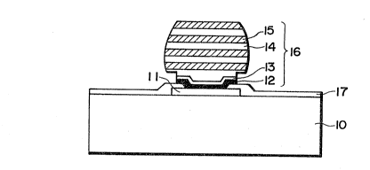
An embodiment of the present invention is described
below with reference to the accompanying drawings. Fig.
3 is a schematic cross section to show a structure of a
semiconductor chip ln the present embodiment. In the
present embodiment, a Ti-W alloy 12 is formed on an Al pad
11 on a semiconductor chip 10~ securing adherence to the
Al pad 11 and serving as a barrier metal to prevent the Al
pad 11 and a Au contact layer 13 from forming an
,'' ~' ' '
'
~0~0~8
SEI ~3-4
1 intermetallic compound in heat during connection
therebetween. The Au contact layer 13 is formed on the
Ti-W alloy 12, which assures superior plating feasibility
in plating of upper Au layer 14 thereon and keeping
adhersnce to the Ti-W alloy 12. A protective layer 17
such as SiN covers an area except for the Al pad 11 on the
semioonductor chip 10. Au layers 14 and Sn layers 15 are
alternately built up on the Au contact layer 13 by the
electroplating method. A multilayered bump 16 is
1~ composed of the Au layers 14 and the Sn layers 15. As
shown in Fig. 4, the uppermost layer in the bump 16a does
not always have to be the Sn layer 15, but may be a Au
layer 14. In this case, if the uppermost Au layer 14 is
sufficiently thin, the uppermost Au layer 14 would melt
by the Au-Sn eutectic alloy reaction during mounting,
which allows sure connection with a moderate pressure.
In case that the uppermost Au layer 14 is formed too thick
to wholly melt, Sn plating should be provided on a tape or
electrode pad. In the present embodiment, the
2~
electroplating method is used for ~ormation of the Sn
layer 15, but the vacuum evaporation method may also be
employed for deposition of Sn laysr 15 (in thickness of
0.1-2.0 ~m).
Since the bump 16 is formed by alternately building
up the Au layers and the Sn layers in the present
embodiment as describ~d, the Au-Sn eutectic alloy
-- 7 --
2~9~0~
SEI 93-4
1 reaction may take place at each boundary surface between
layers in mounting. Then, the entire bump 16 may fully
soften. Even if a plurality of bumps provided on a
semiconductor chip have a slight dispersion of bump
height, secure connection may be obtained with a moderate
pressure.
The bumps are formed on the semiconductor chip in
the above description, but the bumps may also be formed on
an external electrode such as a wiring (circuit)
substrate or a tape used in the TAB method.
Fig. 5 to Fig. 7 show steps of mounting in the flip
chip mounting method. In these drawings, the Ti-W alloy
12, the Au contact layer 13, and the protective layer 17
as shown in Fig. 3 and Fig. 4 are omitted.
A wiring substrate 21 has a conductor portion 211 of
desired pattern and three wiring side pads 212a,212b,212c
connected therewith and made of Au. Also, three bumps
25a, 25b, 25c are formed on pads 221 of a semiconductor
chip 22. Each of these bumps 25a~25c is formed by
- alternately building up three Au layers 23 and three Sn
layers 24 (six layers in total). The uppermos~ layer (as
turning the semiconductor chip 22 upside-down, the
lowermost layer in Fig.5 to Fig.7.) in each bump 25a-25c
is the Sn layer 24.
The wiring substrate 21 is first placed under the
semiconductor chip 22, and the semiconductor chip 22 is
-- 8 --
ï~9~8
SEI 93-4
1 located with the bumps 25a-25c face down. The
semiconductor chip 2~ is aligned with the wiring
substrate 21 such that the bumps 25a-25c may contact with
corresponding wiring side pads 212a-212c, and the
semiconductor chip 22 i5 then pressed. Fig. 5 shows a
step before the bumps 25a-25c come into contact with the
wiring side pads 212a-212c.
Fig. 6 shows a step at which the bumps 25a and 25c on
either end are in contact with the corresponding wiring
~10 side pads 212a and 212c but the shorter bump 25b is not in
contact with the wiring side pad 212b.
In the conventional method, the Au-Sn eutectic
reaction takes place only in the interface portion
between the tip of bump and the wiring side pad, and,
therefore, this step is the end of process, leaving the
bump 25b as defective in contact. In contrast, the Au-Sn
eutectic reaction takes place not only in the interface
between the bump tlp and the wiring side pad but also at
each boundary surface between layers in bump (in this
case, 6 surfaces in total), fully softening the entire
bump in the present invention. Thus, the bump 25b may be
brought into contact with the wiring side pad 212 as shown
in Fig. 7.
Fig. ~ to Fig. 10 show steps of mounting a
semiconductor chip on a printed circuit board by the TAB
method. In these drawings, the Ti-W alloy 12, the Au
_ g _
2~9~0~8
SEI 93-4
1 contact layer 13, and the protective layer 17 as shown in
Fig. 3 and Fig. 4 are omitted.
A lead frame 29 formed in tape has at one end thereof
a lead frame side pad 291 made of Au. A bump 28 is formed
on a pad 271 of a semiconductor chip 27. The bump 28 is
formed by alternately building up three Au layers 23 and
three Sn layers 24 (six layers in total). The uppermost
layer in the bump 28 is the Sn layer 24.
The lead frame 29 is first set above the
semiconductor chip 22 with the lead frame side pad 291
face down, and the semiconductor chip 22 is set with the
bump 28 face up. The lead frame side pad 291 is aligned
to contact with the corresponding bump 28, and the lead
frame 29 is then pressed. F.ig. 8 shows a step before the
bump 28 comes into contact with the lead frame side pad
- 291.
Fig. 9 shows a state in which the bump 28 is in
contact with the lead frame side pad 291 and is securely
connected therewith by the eutectic reaction. Also, in
case that a plurality of bumps arP simultaneously bonded
in the TAB method, the defective contact of bump may be
eliminated in the same manner as described with the
process in the flip chip mounting method. In case that
the uppermost layer of the bump 28 is a Au layer instead
of Sn layer, Sn plating must be preliminarily provided on
the lead frame side pad 291.
-- 10 --
2~0~8
SEI 93-4
1Then, the semiconductor chip 27 electrically
connected with the lead frame 29 is mounted on a printed
circuit board 26. The printed circuit board 26 has a
conductor portion 261 of desired pattern and a wiring
side pad 262 connected therewith. The mounting is made by
soldering of the other end of the lead frame 29 onto the
wiring side pad 262, ending in the state as shown in Fig.
10 .
Next explained is the structure of bump
characteristic in the present invention, including the
height of bump, materials of the respective layers, the
number of the respective layers, and so on.
The materials used for bump may be any two types of
metals capable of undergoing the eutectic reaction.
Specifically, in addition to the combination of Au and Sn
as described, the following combinations may be listed up
as e~amples of the materials for bump. The Au series
includes combinations of base constituents such as Au:Si,
Au:Ge, Au:In, Au:Sb, Au:Ga, and Au:Pb. Also, the Ag
series includes combinations of base constituents such as
Ag:Cu into which Zn, Ni, and/or Cd are added. Further,
the In series includes combinations of base constituents
such as In:Sn, In:~g, an~ In:Pb.
The height of the entire bump changes depending upon
various conditions of semiconductor chip and others
(area, the numbsr of bumps bonded, etc.), usually 10-300
2~i305g
SEI 93-4
1 ~m. The height of bump is not limited to this range.
As for the number of layers in bump, the more the
easier the entire bump softens, but the minimum number is
one layer for each of the two types of metals capable of
undergoing the eutectic reaction. In actual application,
the number of layers must be increased as the height of
the entire bump and the dispersion thereof become
greater. In case ~hat the height of the entire bump is
belo~ 30~ ~m, 3-30 layers are suitable for each metal,
taking into consideration readiness of process in bump
formation, preferably 3-10 layers.
A ratio of thicknesses of two metal layers does not
have to be 1:1 (need not be identical to each other), but
should rather be determined considering an operation
temperature (that is, eutec$ic temperature) in bonding
process. For example, in case of Au:Sn, Sn has a lower
melting point than Au. Therefore, an increase of Sn in
ratio increases a melt part in bump at a lower
temperature. It is preferable that Au:Sn be set at 5:1 to
10:1 in actual applications.
A process for forming a bump is next explained.
Fig. 11 and ~ig. 12 show a first bump forming method
in which a bump is formed using the electroplating method
similar to the technique as described in Reference "
". The reference shows a bump made only of Au, and,
therefore, the bump of the present embodiment is
- 12 -
2 ~ 8
SEI 93-4
1 diff~rent from that in the reference in that the bump is
multilayered with alternate Au and Sn.
An Al pad 101 is formed in a desired area on a
semiconductor chip 100 in which semiconductor elements
are formed, and a protective layer 102 made of SiN is
further formed over the area excluding the Al pad 101 on
the semiconductor chip 100.
Then, a Ti-W alloy layer 103 and a Au contact layer
104 are consecutively deposited over the entire area by
evaporation. A photoresist is then applied over the
entire surface, and a window for bump formation is opened
by the photolithography process.
A Au layer 110 is then formed in thickness of 18 ~m
by electroplatingO A Sn layer 120 is next formed in
thickness of 2 ~m by electroplating. These formation
steps of the Au layer 110 and the Sn layer 120 are
consecutively repeated to form a bump with a desired
height (Fig. 11).
After that, the photoresist 105 is removed, and the
evaporation layers (Ti W alloy layer 103 and Au contact
layer 104) are removed except underneath the bump by
chemical etching (Fig. 12).
In Fig. 12, the Au layers 110 and the Sn layers 120,
four layers each, are formed in bump height of 80 ~m. In
case that there are 300-500 bumps in LSI, the bump height
must be about 200 ~m, and, therefore, the Au layers 110
- 13 -
2~S0~8
SEI 93-4
1 and the Sn layers 120 are to be formed in ten layers each.
Since the plating layer is formed thicker than the
photoresist layer in the above process, the bump is
likely to be formed in "mushroom" shape. Fig. 13 and Fig.
14 show a second bump forming method, in which the bump is
formed with a thicker photoresist to prevent the
horizontal mushroom-like extent of plating layer.
Steps up to the evaporation of the Au contact layer
104 are the same as those in the first bump forming method
lo as described above. A photoresist 106 of shPet dry film
i5 provided (in thickness of not less than 30 ~m) in place
of liquid photoresist. A window for bump formation is
; opened by the photolithography process, and Au layers 111
and Sn layers 121 are alternately formed by
electroplating (Fig. 13).
After that, the photoresist 106 is removed, and the
evaporation layers (Ti-W alloy layer 103 and Au contact
- lay~r 104) are removed except underneath the bump by
chemical etching (Fig. 14).
Fig. 15 to Fig. 17 show a third bump forming method,
in which a bump is formed by evaporation. Steps up to the
window opening for bump formation are the same as those in
the first bump forming method as described. After the
window opening, Au layers 112 and Sn layers 122 are
alternately deposited by the evaporation method.
Further, a phbtoresist 107 is formed on an area under
2 ~ 5 ~
SEI 93-4
1 which a bump is to be formed (Fig. 15). Unnecessary
portions of the Au layers 112 and the Sn layers 122 are
removed with the photoresist 107 serving as a mask (Fig.
16).
After that, the photoresists 105 and 107 are
removed, and the evaporation layers (Ti-W alloy layer 103
and Au contact layer 104) are removed except undernea~h
the bump by chemical etching (Fig. 17).
Fig. 18 and Fig. 19 show a fourth forming method, in
which a bump is formed by evaporation and lift-off. In
this case, a photoresist 106 of sheet dry film is used
instead of liquid photoresist, in the same manner as in
the second bump forming method. Steps up to the window
opening for bump formation in the photoresist 106 are the
same as those in the second bump forming method.
After the steps, Au layers 113 and Sn layers 1?-3 are
alternately formed by evaporation (Fig. 18). Then,
unnecessary portions of the Au layers 113 and the Sn
layers 123 are lifted off by removing the photoresist
106. Further, the evaporation layers (Ti-W alloy layer
103 and Au contact layer 104) are removed except
underneath the bump by chemical etching (Fig. 19).
The evaporation method require~ a longer time in
formation of layer than the electroplating method, if the
thickness is identical. Thus, the evaporation method is
inferior in productivity to the elec~roplating method
-- 15 --
SEI 93-4
1 when it is applied to formation of thicker bump. The two
method may be suitably combined in formation of bump. For
example, in case of forming a bump made of Au (in
thickness of 18 ~m):Sn (in thickness of 2 ~m), Au layers
may be formed by the electroplating method and Sn layers
by th0 evaporation method.
From the invention thus described, it will be
obvious that the invention may be varied in many ways.
Such variations are not to be regarded as a departure from
the spirit and scope of the invention, and all such
modifications as would be obvious to one skilled in the
art are intended to be included within the scope of the
following claims.
~0
- 16 -
.