Note: Descriptions are shown in the official language in which they were submitted.
CA 02095119 2001-03-29
72235-37
1
BACKGROUND
1. Field of the Invention
This invention relates generally to electrical
connectors. More particularly, the invention relates to an
electrical connector which utilizes the mating of a tapered
contact element with the conductive rim of a hole for providing
an electrical connector function. The invention further
relates to electrically connecting a first board, cable, wire,
or other current carrying means which is coupled to the contact
element, to a second board, cable, wire or other current
carrying means on which the conductive rim of the hole is
located.
1. Prior Art
The electrical connector arts are crowded arts with
many categories and subcategories of connectors. Besides the
connectors of the art discussed in the Prior Art section of the
parent application hereto, other types of connectors are known
such as ribbon cable connectors, flex circuit connectors, pin
and socket connectors, rack and panel connectors, zero
insertion force connectors, coaxial cable connectors,
insulation displacement connectors, quick connect/disconnect
connectors, card edge connectors, board to board connectors,
board to wire connectors, surface mount connectors, etc.
Common to many of the connectors is that they include a male
component which is coupled to a first device which is to be
connected and a female component which is coupled to a second
device which is to be connected, wherein the male and female
components are arranged to mate. While two piece (i.e. male
and female component) connectors are generally effective for
their purposes, they are costly because they require two
72235-37
CA 02095119 2001-03-29
2
separate parts for accomplishing a single connection. In
addition, where the connectors have multiple pins, connection
and disconnection becomes difficult because of the forces
involved, and the male connector is easily damaged during
removal or reinsertion. Also, because a connector piece is
required on each of the devices to be connected, the two piece
connectors often take up valuable "real estate".
SUMMARY OF THE INVENTION
The invention provides an electrical connector for
providing a semipermanent electrical connection between the
conductive rims o.f holes of a first object and the conductive
rims of holes of a second object, said first object and second
object being substantially parallel each other, said electrical
connector for use with a fastening means which fastens said
electrical connector to or between said first and second
objects, said electrical connector comprising: a plurality of
spring contact element means, at least two of said plurality of
spring contact element means being electrically isolated one
from the other, each spring contact element means having a
first tapered contact portion for mating with a conductive rim
of a said hole of said first object, a second tapered contact
portion for mating with a conductive rim of a said hole of said
second object, and a spring portion coupled to said first and
second tapered contact portions, said spring portion being
laterally tolerant for permitting at least one of said first
tapered contact portion and said second tapered contact portion
to move laterally in a substantially free floating manner so as
to seat in the conductive rim of the hole in the object with
which it mates; and a dielectric housing for housing said
plurality of spring contact elements, said dielectric housing
comprising a front wall which is substantially parallel said
CA 02095119 2001-03-29
72235-37
3
first object when said electrical connector mates with said
first object, said front wall having a plurality of first
apertures for permitting at least a portion of said first
tapered contact portions of said plurality of spring contact
element means to extend therethrough.
The invention also provides an electrical connector
for mating with conductive rims of holes of a board, and for
use with a fastening means which fastens said electrical
connector to said board, said electrical connector comprising:
a) a plurality of contact element means, each of said plurality
of contact element means having a first portion for making
electrical contact with conductor means other than said circuit
board, and each contact element means having a tapered contact
portion for mating with one of said conductive rims of said
circuit board; b) a dielectrical housing for housing said
plurality of contact element means, said dielectrical housing
comprising a front wall which is substantially parallel said
board when said electrical connector mates with said board,
said front wall having a plurality of apertures shaped for
permitting at least a portion of said tapered contact portions
of said plurality of contact element means to extend
therethrough and for stopping said contact element means in
desired locations such that said contact element means are
preloaded; and c) first make, last break means for causing a
particular of said plurality of contact element means to
contact a particular conductive rim before others of said
plurality of contact element means contact others of said
conductive rims.
The invention further provides an electrical
connector for mating with conductive rims of holes of a circuit
board, comprising: a) a plurality of contact element means,
CA 02095119 2001-03-29
72235-37
3a
each contact element means having a spring portion which makes
electrical contact with conductor means other than said circuit
board, and each contact element means having a tapered contact
portion coupled to said spring portion for mating with one of
said conductive rims of said circuit board, each contact
element being laterally tolerant for permitting said tapered
contact portion to move laterally in a substantially free
floating manner so as to seat in the conductive rim of the hole
in the object with which it mates; b) fastening means for use
in fastening said electrical connector to said board to keep
said plurality of tapered contact elements mated with said
conductive rims; and c) a dielectric housing for housing said
plurality of tapered contact elements.
The invention further provides an electrical
connector for connecting conductors of a ribbon cable with
conductive rims of holes of a board, comprising: a) a
plurality of contact element means, each contact element means
having a insulation stripping tail means for making contact
with a conductor of a ribbon cable, a tapered contact portion
coupled for mating with one of said conductive rims of said
board, and spring means coupling said insulation stripping tail
means and said tapered contact portion; and b) fastening means
for use in fastening said electrical connector to said board to
keep said plurality of tapered contact elements mated with said
conductive rims.
The invention further provides an electrical
connector for mating with conductive rims of holes of a board,
comprising: a) a plurality of contact element means, each
contact element means having a wire formed tapered contact
portion for mating with one of said conductive rims of said
board, said wire formed tapered contact portion being radially
~
~ 72235-37
CA 02095119 2001-03-29
3b
compliant so as to provide substantial wipe upon mating in said
conductive rim, and said tapered contact portion being formed
to angularly engage opposite sides of the conductive rim; and
b) fastening means for use in fastening said electrical
connector to said board to keep said plurality of wire formed
tapered contact elements mated with said conductive rims
wherein each said contact element means has a post, said wire
formed tapered portion coupled to said post, each post coupled
to conductive means other than said conductive rims of said
holes of said board.
The invention further provides an electrical
connector for connecting a flexible printed circuit to
conductive rims of holes of a circuit board, comprising: a
bent beam spring for fastening said flex print to said circuit
board, wherein said circuit board includes second holes, said
bent beam spring :includes at least two legs which engage said
second holes of said circuit board, and paid flexible printed
circuit is embossed with conductive tapered contact portions
for mating with said conductive rims.
Each aspect of the invention may take many forms.
The spring portion of the contact elements may have, e.g., a,
u, s, or z shape. The tapered contact portion of the contact
elements can take the form of a bifurcated cone or a compliant
bent wire. Also, the portion of the contact elements which
make electrical contact with the first object may take the form
of, e.g., a post for coupling to holes, prongs for stripping
insulation, a spring for surface contact, or any of many
tapered forms such as described with reference to the tapered
contact portion for coupling to conductive rims. The housing
for the tapered contact elements may be arranged to serve
various purposes. For example, by making the wall section of
CA 02095119 2001-03-29
72235-37
3c
the housing through which the contact elements extend
nonuniform, a "first make, last break" function can be
accomplished. A "first make, last break" function may also be
accomplished by a hinged housing. Also, the housing for the
contact elements may be one piece or two piece, rear loaded or
front loaded.
Other advantages of the present invention will become
evident upon reference to the detailed description in
conjunction with the provided figures.
BRIEF DESCRIPTION OF THE DRAWINGS
Fig. 1 is a perspective view of a column section of a
first embodiment of the connector invention prior to insertion
of a preformed spring contact elements into the housing.
WO 92/08258 0 1 PCT/US91108009 ~,,
2
4
Fig. 2a is a top view of the first embodiment of the
connector invention showing a row of contact elements with
second ends extending appropriately out of the housing:
Fig. 2b is a front view of the first embodiment of the
connector invention.
Fig. 3a is a cross sectional view of the first embodiment
of the connector invention through line A-A of Figure 2b.
Fig. 3b is an enlarged cross sectional view of the self-
centering tapered funnel of the housing shown in Fig. 3a with
a contact element located therein in an unengaged extended
position, and in engaged depressed positions.
Fig. 3c is a partially cut-away top view of the connector
of Figure 3a taken along line C-C of Fig. 3a.
Fig. 4a is a perspective enlarged view of the tapered end
of a single split-cone contact element in contact with a
plated through hole.
Fig. 4b is a cross sectional view of the tapered end of a
single split-cone contact element of the first embodiment of
the connector through line B-B of Fig. 4a.
Fig. 4c is a force diagram for a typical contact element
of the connector of the invention, showing both axial
insertion (hold-in) and mating contact normal forces.
Figs. 5a-5f are diagrammatic representations of six
different embodiments of the spring portion of the contact
element of the invention;
suesTrTU~r~ s~rr=E-r
O 92/08258 PCT/US91/08009
Fig G3'g ~~ a~n ~ loded view of a second embodiment of the
connector invention having a housing and utilizing the contact
of Fig. 5f;
Fig. 5h is a partial cross-sectional view of the
assembled connector of Fig. 5g;
Fig. 6a-6d are diagrammatic representations of four
different embodiments of the tail portion of the contact
element of the invention;
Fig. 6e is a cross section through a connector according
to the invention utilizing the contact element of Fig. 6a;
Figs. 6f-6h are exploded views of different connectors
according to the invention utilizing the contact element of
Fig. 6b;
Figs. 6i and 6j are cross sections through connectors of
the invention utilizing the contact elements of Fig. 6d;
Figs. 7a and 7b are front and side views of a wire tip
embodiment of the contact element of the invention;
Fig. 8 is a cross-section through a connector of the
invention utilizing a wire formed contact element, where the
housing of the connector is used as a mandrel for the forming
of the spring loaded contact element;
Fig. 9 is a cross section through a housing for a
connector of the invention having a first make, last break
~ feature formed by the housing itself;
Fig. 10 is a diagrammatic perspective of a connector of
the invention utilizing a hinged housing;
SUBSTITUTE SHEET
WO 92/08258 ~ PCT/US91/08009
6
Figs. 11a and 11b are cross sections through a straight
through embodiment and a perpendicular embodiment of a female
mating connector for the connector of the invention;
Figs. 12a and 12b are cross sections through non-solder
straight and right angle permanent connectors respectively;
Figure 13 is a cross section of a flex-print to board
connector utilizing the tapered contact to conductive rim
mating according to the invention; and
Figure 14 is a cross section of a connector useful for
board to board applications where different board to board
distances are accommodated.
DETAILED DESCRIPTION OF THE PREFERRED EMBODIMENT
Before describing the-preferred embodiments of the
invention, it should be appreciated that the connector
invention as described herein is for mating with the
conductive rims of the holes of an object. The holes need not
be round, as connection to rims of other shaped holes (even if
the rim is not continuous) is envisioned. Neither must the
holes be through holes or plated through holes, as connections
with blind holes or holes having only a plated rim are
envisioned. Further, the object in which the holes are
located need not be a printed circuit board, as connection to
other objects (e. g., flex circuits) is envisioned.
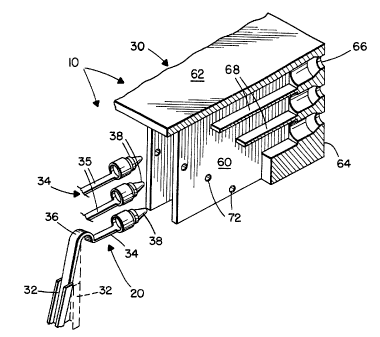
Figures 1, 2a, 2b, 3a - 3c, and 4a - 4c show a first
connector embodiment of the invention which is a right angle
connector. The connector assembly 10 typically comprises a
plurality of contact elements 20, and a dielectric housing 30
for housing the contact elements. The contact elements 30 are
spring pins with first ends 32, second ends 34, and a middle
bend section 36. The first ends 32 of pins 20 extend through
holes 39 in a daughter board 40 and are preferably soldered to
the back side 41 of the daughter board. At least a portion of
the first ends 32 is preferably v-shaped to help align the
first ends in the holes 39 of the daughter board 40. The
SIJB~~'fTi !~~'E SEE ~
O 92/08258 PCT/US91/08009
2085119
7
shape of first ends 32 also provides stii:fness, and helps in
preloading the contacts as will be discussed hereinafter.
The second ends 34 of the contact e:Lements 30 are
basically comprised of a neck portion 35 which may be channel
shaped for stiffness, and a tapered contact portion 38. As
seen in Fig. 3b, connecting the neck portion 35 to the contact
portion 38 is an angled portion 37 which acts in conjunction
with the housing to provide self-alignment and preloading as
will be described hereinafter:
The mid-sections 36 of pins 20 are preferably crimped to
cause pins 20 to form a spring. As shown in Fig. 1, pins 20
are preferably crimped to first form a one hundred eighty
degree bend and then a minus ninety degree bend, and are thus
essentially bent through ninety degrees. If desired, a simple
bend of ninety degrees could be used, provided mid-sections 36
form spring elements. As seen in Fig. 3a in phantom, when
contact portions 38 of second ends 34 of pins 30 engage the
mother board 50, the mid-sections 36 resp_liently deflect away
from the mother board 50; i.e. the mid-sEactions 36 are
compliant along the mating axis'. In so doing, the mid-
sections 36 provide pins 30 with a mating force.
As seen in Fig. 4a, the contact portions 38 of the second
ends 34 of contact elements 20 are tapered in cross section,
with the cross section becoming larger further away from the
end or tip of the contact element. The contact portions 38
are used to make contact with the plated through holes 51 of
the mother board 50. Where the contact ~>ortions 38 of the
p second ends 34 are the preferred split (x>ifurcated) cones (as
seen in Figs. 4a and 4b), contact is mads~ between the
a connector 10 and the mother board 50 at t:wo points 53a, 53b
(radius contact "points") for each contact element 20 and
through hole 51. The contact is made between the tapered
portion (i.e. the contact portion 38) of the contact element
20 and the rim of hole 51; i.e. the circumference of the hole
SUBSTITUTE SHEET
WO 92/08258 1 ~ 9 PCT/US91/08009
8
51 at the surface 55 of the mother board 50. In making
contact, because contact portion 38 is bifurcated, it
resiliently compresses as it is pushed into hole 51, and
therefore extends into hole 51 further than it might have
otherwise. As a result, the surface of contact portion 38
wipes along the rim of hole 51 as it makes contact providing
desired "wipe" and enhanced contact.
As seen in idealized force diagram of Fig. 4c, the use of
contact elements having tapered contact portions 38 which
extend into plated through holes 51 of a mother board
magnifies the "normal" force relative to the axial holding or
mating force. In particular, and by way of example only, if
the axial mating force FA is fifty grams, the axial mating
force at each of the two points of contact is seen as twenty-
five grams (FA/2). Of course, the mother PCB must assert an
equal but opposite force of twenty-five grams at each point.
However, the equal but opposite force must be asserted as a
component of a force which is perpendicular (i.e. normal) to
the point of contact. Thus, at each of the two
contact points, the mother board 50 provides a normal contact
force FN/2 (shown as the hypotenuse of the triangle). Each
normal contact force is the result of two perpendicular
forces; an axial force of twenty-five grams opposite to the
mating force (as required to provide an equal but opposite
force to the axial mating force); and a force perpendicular to
the axial force. As will be appreciated, the perpendicular
forces to the axial forces are equal and opposite each other
and therefore cancel.
Assuming that the contact portion 38 tapers at an angle
of fifteen degrees relative to the axial direction, in order
for a twenty-five gram axial force opposite to the axial
mating force to be generated at each point of contact, a
resultant normal force (FN/2) of one hundred grams (twenty-
five grams divided by the sine of fifteen degrees) is
generated at each point. Thus, for a pin having a total axial
~~$~J~~~i ~ i ~ aS~"~~~~
WO 92/08258 PCT/US91/08009
2p g51 19 n_r_.
9
mating force of fifty grams, the normal force generated is two
hundred grams. More generically, the normal force generated
at each point of contact is equal to the axial force at that
contact point divided by the sine of the taper angle of the
tapered contact portion 38 of the pin 20., The smaller the
taper angle , the larger the normal force generated.
Regardless of the taper angle, the total normal force
generated by all the contact points is a7Lways greater than the
axial insertion force as FN/FA = 1/sin
Returning to Figs. l, 2a, 2b, and 3a-3c a single piece
dielectric housing 30 is seen. The housing 30 includes side
walls 60 which separate and electrically insulate each column
of contact pins 20; the side walls 60 extending
perpendicularly from top wall 62. Also extending
perpendicularly from top wall 62 is front: wall 64 having a
plurality of openings 66 for permitting at least a portion of
tapered contact portions 38 (and preferax>ly the entire tapered
contact portion) of contact pins 20 to a}wend therethrough.
Openings 66 are preferably tapered funnels which are arranged
to interact with the angled portion 37 of the second ends 34
of the contact pins as will be hereinafter described.
Extending rearward from the front wall 69: in a manner parallel
to top wall 62 are a plurality of pin set>aration walls 68
(also called "guide walls") which guide t;he second ends 34 and
contact portions 38 of pins 20 into theix° preloaded position,
and electrically insulate one pin contact: from another.
Because different rows of pins 20 traver~~e different lengths
(as seen in Figs. 1 and 3a), the lengths of separation walls
68 are varied accordingly. Preferably, each guide wall
extends slightly past the middle bent portion 36 of the pin
contact below it, but only as far as the second end 34 of the
pin above it.
Fig. 3b explores the axial and lateral tolerances built
into the connector contact pins relative to the holes of the
mother board. As shown, when the contact. pins are not
SUBSTITUTE SHEET
WO 92/08258 PGT/US91 /08009
engaging the mother board, angled portions 37 contact the
funnel-like openings 66 and thereby center themselves therein
in a nominal position. By arranging openings 66 to be smaller
in cross section than the cross section of the widest part of
angled portion 37, the openings 66 act as a stop to the
contact spring pins 20 to cause the spring pins to be
preloaded in the housing, as will be discussed hereinafter.
In the preloaded position, the contact portions 38 of the pins
extend out of the housing 30 by a desired amount. When the
contact pins 20 engage the mother board holes, the pins 20 are
pushed backward (as seen in phantom) such that the angled
portion 37 of the second ends 34 of the pins no longer
contacts the funnel-like openings 66 of the housing 30. As a
result, lateral movement of the second end of the pin is
expedited in all directions, as the passage for the second end
of the pin defined by adjacent side walls 60 and adjacent
guide walls 68 of the housing 30 is wider than the second ends
34 of the pins. As will be appreciated by those skilled in
the art, the further pins 20 are pushed backward, the more
second ends 34 can move laterally in any direction in the
housing passage. As a result, a tolerance zone or range for
the misalignment of a pin relative to a hole is provided which
can approach the radius of the hole in size (provided the
housing passage and funnel-like opening are large enough).
Also, as seen in Fig. 3b, the tapering of the contact portion
38 of pin 20 provides tolerance relative to the hole diameter,
as contact along the tapered surface of the contact portion 38
is guaranteed.
As seen in Figs. 1, 3a, and 3c, side walls 60 of housing
preferably include sidewall locking tabs 72 (preferably two
per contact) which hold adjacent rows of contacts in a
preloaded manner at different fixing points relative to the
daughter board 40 but at identical fixing points relative to
the ninety-degree bend portion 36 of the contact elements 20.
The locking tabs 72 provide a restriction between adjacent
side walls 60 through which the v-shaped first end 32 of pins
20 are forced during assembly. After the v-shaped first end
SUBSTITUTE Si~EET
WO 92/08258 PCT/US91/08009
2pg5119
1
11
32 deforms and passes through the tabs 72, they cannot return
past the tabs 72. Thus, locking tabs 72 act to provide a
preload to the spring contact elements 20 as the spring
. contact elements 20 are fixed in location on one end by the
contact of angled portion 37 with the funnel-like opening 66,
. and on the other end by locking tabs. The locking tabs 72
also act to establish a fixing point which fixes a portion of
first end 32 (the portion between the locking tab 72 and the
daughter board) against movement in the axis of insertion. As
a result, the tabs 72 act as a strain re7.ief for the first end
32 - daughter board solder joint, as the first end 32 will not
substantially move below tab 72. The v-:shape of first end 32
also helps to stiffen first end 32 and to prevent movement at
the solder joint.
By locating the locking tabs 72 sucrn that pins of
different rows have approximately the same spring length
between the fixing point and the bend (aa seen in Figs. 1 and
3a), equal bearing forces between the contact portions 38 of
pins 20 of different rows of the connector and the holes 51 of
the mother board 50 are assured.
Housing 30 may also include at least: one integral guide
pin 74. Guide pin 74 may act as a ground pin by having a
ground wire (not shown) wrapped around it, and/or a make first
pin for the connector. Typically, and as> shown in Figs. 2a
and 2b, two guide pins 74 are located on either end of the
connector and extend along the same axis as the second portion
of pins 20. Preferably, the guide pins extend out further
than the contact portions 38 of pins 20 a:nd thus act in a
shielding or protective capacity, although other protective
means such as retractable shrouds (e.g. Live hinges or
protective flaps) could be utilized. The: guide pins 74 are
preferably arranged such that they exten6l into mating holes in
the mother board, with the diameter of the mating holes being
as large as or slightly greater than the diameter of non-
tapered section of the guide pin. While at least one guide
SUBSTiTUT~ SH~~r
WO 92/08258 PCT/US91 /08009
12
pin is preferably integrally molded with the connector, other
guide pins may have a threaded end, and are held in place in
the housing 30 by rivets 76. If desired, first and second
guide pins may be oval in cross-section and oriented
perpendicularly with respect to one another. In this manner,
one guide pin acts as a horizontal guide, while the other acts
as a vertical guide.
Turning to Figures 5a-5f, six different spring contact
elements 220a, 220b,... which are useful for parallel board to
board connectors are seen. Each of the spring contact
elements 220 has a first tapered end 221, a middle portion
236, and a second tapered end 223. The tapered ends 221 and
223 are used to mate with the conductive rims of a board. The
middle portions 236 of each of spring contact elements 220a,
220b,... effectively provide the spring action when the spring
contact elements are loaded in a housing. The middle portion
236a of spring element 220a of Fig. 5a is a u-shaped spring,
while the middle portion 236b or spring element 220b of Fig.
5b is a z-shaped spring. The z-shaped spring provides some
symmetry as opposed to the u-shaped spring. Middle portions
236c and 236f of spring elements 220c and 220f are s-shaped
springs which also provide symmetry. In addition, with the
severe s-shape of spring element 220f, when tapered ends 221f
and 223f are pressed together, the s-shaped middle portion
236f actually decreases in width rather than increasing as
would be the case with the spring elements of Figures 5b and
5c.
The middle portion 236d of spring element 220d of Fig. 5d
is a bellows (i.e. a continuous u-shaped spring) which has low
inductance and hence a different electrical characteristic
than the other spring elements. The middle portion 236e of
spring element 220e of Fig. 5e, is formed by welding the tails
of two identical single tapered elements together at weld 229.
With spring element 220e, the connection of parallel boards
having different spacings can be accommodated with a single
SI~BSTITt3T~ SHEET
WO 92/08258 PCT/US91/08009
2pg5119
13
contact element tooling, as the tails may be welded at
different points to form spring elements of different lengths.
It should be appreciated that the locations of joining of the
tapered ends 221 and 223 to the middle portion 236 in each of
the spring elements of Figs. 5a-5e are preferably chosen to
m provide the most stability for the spring element; i.e. to
reduce torque to a minimum when the tapered portion mates with
a rim.
Turning to Figures 5g and 5h, a connector with a
plurality of spring contact elements 220f and a two piece
housing 230 is seen. As seen in more detail in Fig. 5h, each
piece 230a and 230b of housing 230 has a plurality of holes in
which the tapered contact and the middle portion of the spring
is housed. In particular, the holes of the housing are
comprised of a tapered section 237 through which the tapered
contact (221 or 223) extends, and a larger opening 239 in
which the s-shaped spring 236f is housed. Enough room is
provided in opening 239 to guarantee that the s-spring 236f
will not touch the housing in its preloaded and mating
positions. Pieces 230a and 230b of housing 230 may be
identical, assembled back-to-back, and held together via sonic
welding, glue, or other means. On the other hand, if desired,
pieces 230a and 23ob may be provided with reciprocating posts
274a and post receivers 274b for a friction or press fit.
Regardless, the housing 230 preferably includes posts 274c
which act as guide pins for mating with circuit boards 250.
It should be appreciated that the spring contact elements
of Figs. 5a-5f may be provided with two tapered ends for
tapered-end-to-rim mating with holes of two boards, or may be
provided with one tapered end for tapered-end-to-rim mating
and a second end (tail portion) with a different configuration
° for connection or mating to any desired conductive device.
Examples of spring contact elements with different tail
portions are seen in Figs. 6a-6d. In Fig. 6a, a spring
contact element 320a is shown with a tapered contact portion
SUBSTITUTE SHEET
WO 92/08258 ~ ~ PCT/US91/08009
14
321a for mating with the conductive rim of a hole in circuit
board 350b, a spring portion 336a, and a tail portion 323a.
The tail portion 323a includes a solder tail 301 and a stop
302, with the tail 301 being arranged to be press fit and/or
soldered into a hole 303 (as seen in Fig. 6e) of circuit board
350a, or surface mounted (SMT) on the board surface. The
connector utilizing the contact 320a, as seen in Fig. 6e, has
a one piece housing 330 with a tapered opening 337e for the
tapered contact portion 321a, and an opening 339e of slightly
larger width for housing the spring 336a. Guide pins 374c are
provided for mating with holes in circuit boards 350a and
350b.
The spring contact element 320b of Fig. 6b, also includes
the tapered contact portion 321b, a spring portion 336b, and a
tail portion 323b. However, the tail portion 323b is
effectively part of the spring portion 336 and provides
preloading to establish electrical contact with a conductive
pad, wire, or surface. The tail portion 323b may be a single
piece or bifurcated as shown in Fig. 6b. Spring contact
element 320b is easily formed and plated on a carrier strip
(shown in Figs. 6f-6h) which may be broken away when the
tapered contact portion 320b is inserted into a suitable
housing 330.
As seen in Figs. 6f-6h, the spring contact element 320b
is advantageously used in several different manners. In Fig.
6f, a connector which can connect two aligned circuit boards
is shown. The connector includes two sets of tapered contact
elements 320b (shown with their carrier strips 304 which are
removed upon loading), a spacer 305 with conductive pads or
wires 306, and a housing 330 having pieces 330a and 330b. The
spacer 305 is provided with shaped rails 307, and the housing
pieces 330a and 330b are provided with grooves 308 for
permitting housing pieces 330a and 330b to be snapped into
spacer 305 to form a unitary assembly. If desired, the
connector housing and spacer as well as the circuit board 350
StlSST~TUTE S~iEET
WO 92/08258 PCT/US91/08009
~~ ~ ~ ~ ~ ~ 15
may be provided with holes to permit the connector to be
attached to the circuit board via screws 309f and nuts 311f.
Guide pins 374c may also be provided. When loaded, the tails
323b of contact element 320b are in cont<~ct with different
wires or pads 306 of the spacer 305. The spacer 305 includes
a internal connective wires to electrically connect each pad 306
on one side of the spacer to one or more associated pads on
the other side of the spacer. The spacer 305 may be
manufactured to different thicknesses to accommodate different
board to board spacings.
Figs. 6g and 6h show the spring coni~act element 32Ob used
in a PC board to surface mount board connector and in a PC
board to flex circuit connector. In Fig.. 6g, the surface
mount board 305g having bottom ide circuit pads 312g is
included in the connector by providing a plastic strain relief
piece 313 and a metal clip 314 which sit atop the the SMT
board 305g and are held by nuts 3118 and screws 309g which
extend therethrough and through the housing 330a and PC board
350. The metal clip 314 is provided to maintain flatness and
contact force. Rails 307g on the metal clip 314 grab grooves
308g on the housing 330a for a snap fit.
As seen in Fig. 6h, a flex circuit 350h, which includes
top and bottom pads 312-ih and 312-2h, i:~ incorporated into a
connector. The connector of Fig. 6h also includes two sets of
contact elements 320b carried on carrier strips 304, housing
pieces 330a and 330b. When the contact s:lements 320b are
placed in the housing, 330, the carrier :>trips are preferably
removed. The entire assembly is fastened with screws 309h and
nuts 311h in a similar manner to the assemblies of Figs. 6f
and 6g.
Turning to Figs. 6c and 6d:, contact elements 320c and
320d which have tail portions adapted for ribbon cable
connection (i.e. insulation displacement) are seen. The
contact elements 320c and 320d are substantially identical,
SUBSTITUTE SHEET
WO 92/08258 ~ PCT/US91/08009
16
except that the tail portion 323c of Fig. 6c is substantially
coaxial with the contact portion 321c, while the tail portion
323d of Fig. 6d is substantially perpendicular to the contact
portion 321d.
In Figs. 6i and 6j, the contact element 320d shown in
Fig. 6d is used in two different configurations for two
different connectors. In Fig. 6i, a two piece housing (330a,
330b) is utilized to house contact element 320d, having
contact portion 321d, spring portion 336d, and tail portion
323d. The tail portion 323d is perpendicular to the contact
portion and has two prongs which act to strip insulation from
a ribbon cable 350i. A clamp 314i is provided to guarantee
permanent engagement between the ribbon cable 350i and the
tail portion 323d of the contact element 320d.
In Fig. 6j, two identical contact elements 321-ld and
321-2d are provided with one of the elements rotated one
hundred eight degrees relative to the other, and with the
elements having their tail portions 323d bent at different
locations (309-1j and 309-2j). With such an arrangement, the
insulation stripping tail portions of the adjacent contact
elements are not directly adjacent each other; the non-
adjacency of contacts between wires of a ribbon cable being a
requirement for most ribbon cable connectors due to the
proximity of the wires.
Turning to Fig. 7a, a tapered contact element 421 made
from wire is seen in a housing 430 with an opening. The
tapered contact element 421 is effectively bifurcated with
segments 401, 402 and 403 acting as a first portion, and
segments 405, 406, and 407 acting as a second substantially
independent portion. Segment 401 of the tapered contact
element is anchored in a supporting post, and segment 402 is
bent at an angle of about one hundred twenty degrees relative
to segment 401. Segment 403 is bent at an angle of
approximately ninety degrees relative to segment 402 and
_ _,
WO 92/08258 PCT/US91/08009
20 9 5 1 1~9
17
terminates at point 404 where the second portion of the
tapered contact element 421 also terminates. The relative
geometries of segments 407, 406 and 405 mirror those of
- segments 401, 402, and 403. However, as seen in Fig. 7b, the
bending of segment 402 relative to segment 401, and segment
406 relative to 407 is slightly different: (i.e. opposite) in a
second plane such that segments 402 and X606 can extend past
each other. As seen in Fig. 7a, segment: 402 and 406 touch
each other as they extend past each other, although such
touching is not required. Likewise, in order that segments
403 and 405 meet at point 404, the bending of segment 403
relative to segment 402 in a second plane' is the opposite of
the bending of segment 405 relative to segment 406 in that
second plane.
With the wire formed tapered contact: element 421, the tip
404 has three degrees of freedom. When :segments 403 and 405
make contact with the rim of a hole, segments 403 and 405 are
pushed backward, causing the angles between segments 401 and
402, segments 407 and 406, segments 402 and 403, and segments
405 and 406 to be decreased, and the ang7.e between segments
403 and 405 to be increased. Thus, when the wire formed
tapered contact element 421 engages the rim of a hole, the
tapered portion in part compresses and in part retracts and
enhances contact. In addition,'some rotation of the contact
element 421 relative to the rim of the hole can occur which
further enhances contact. Effectively, then, because wire
formed tapered contact element 421 has a tip which has
flexibility in several directions, the ti.p may act both as the
contact portion and the spring portion of the contact element.
No spring section is required for contact: element 421 beyond
the contact portion, although a spring section may be used.
It will be appreciated that the wire: formed tapered
contact element may be provided with different post
assemblies. For example, the segments 401 and 407 can be
crimped in a split post 409 as seen in Fig. 7a, force fit or
SUBSTITUTE SHEET
WO 92/08258 ~ PCT/US91/08009
18
soldered to a.post having holes therein, welded to the outside
of a round or square post, etc.
It will further be appreciated that depending on the
properties of the wire of the wire formed tapered contact
element 421 of Figs. 7a and 7b, and also depending upon the
angles between the segments themselves, and the angle between
segments 401 and 407 and the post 409, the wire formed tapered
contact element 421 may be primarily radially compliant as
opposed to being primarily axially compliant like the tapered
contact elements of Figs. 3a, and 5a-5f. In other words, with
the arrangement shown in Figs. 7a and 7b, when the wire formed
tapered contact element 421 contacts the rim of a hole, point
404 (the tip) of the contact element moves back very little,
as opposed to the point of the bifurcated spring contact
portion of Fig. 3a. Rather, the angle between segments 403
and 405 changes so that the segments 403 and 405 (which
effectively form a cross section through a tapered cone) are
compressed while they ride down the hole. The compression of
the "cone" provides a high degree of wipe during mating. In
Fig. 3a, there is more axial compliance and less radial
compliance (although the bifurcated cone is radially
compliant), and as a result, there is less wipe. Thus,
depending upon the particular circumstances, it may be
desirable to use a connector having a wire formed tapered
contact element such as in Figs. 7a and 7b, or a contact
element such as in Figs. 3a, and 5a-5f which provide more
axial compliance. It should be noted, that regardless of the
degree of axial versus radial compliance desired, lateral
compliance in the contact element is also desired to give
alignment tolerance between the contact element and the hole
rim.
Another wire formed contact element 520 is seen in Fig.
8. In the embodiment of Fig. 8, the housing 530a may be used
as a mandrel on which the spring contact 520 is at least
partially formed. The wire formed spring contact element 520
SUBSTITU'~E SI~iEE'~'
O 92/08258 2 0 9 ~ 1 1 9 ~ T PCT/US91/08009
19
includes segments 501, 502, 503, 505, anc~ 506, with segments
503, 505, and 506 preferably preformed. Segment 501 acts as
the tail segment and is held in place by housing portions 53oa
and 503b. In forming the contact element:, as indicated in
Fig. 8, segment 502 is bent around housing 530a at about
ninety degrees relative to segment 501. Then; segment 502 is
held against the housing 530a at point 5»9 and overbent along
ramp 517 while segment 506 engages ramp _°>13 of housing 530a.
Upon releasing the contact element at point 519, segment 502
springs back into the position as shown in Fig. 8, while
segment 506 disengages ramp 513. With segments 503, 505, and
506 already preformed, the wire formed tapered spring contact
element 520 can be used to engage the rim of a hole of a PCB
550 or the like. Upon engaging the rim of a hole, portions
502, 503, 505 and 506 of the spring contact element are forced
backward. As a result, portion 506 of the spring contact
element 521 engages ramp 513, and portions 505 and 503 are
spread relative to each other, thereby enhancing contact and
mating.
If desired, the connector of Fig. 8 may have a second
section which is the mirror image of that: shown. In this
manner, board to board connection may be made without having
any fixed connections.
Because of the tolerances available with the mating of a
tapered contact element with a rim of a hole, connectors
utilizing such a mating scheme can be readily provided with
various first mate {make), last break arx-angements. For
example, as seen in Fig. 9, a connector is shown with a first
contact element 620a having bifurcated conical contact portion
621a, and a second contact element 620b having bifurcated
conical contact portion 621b. In accord with the embodiment
of Fig. 3b, each contact element has an angled surface 637 for
centering and spring loading purposes. Also, the housing 630
for the contact elements includes similarly angled surfaces
666a, and 666b for engaging angled surfaces 637. However, in
SUBSTlTtJTE SHEET
WO 92/08258 ~ PCT/US91/08009 _.
order to provide a first make, last break arrangement, the
angled surfaces 666a and 666b of the housing 630 are not
identical. As shown in Fig. 9, angled surface 666b is molded
closer to the front face 664 of the housing 630 than is angled
surface 666a. This difference is more easily seen by
comparing the length of opening surfaces 669a and 669b. As a
result of this difference, the contact portion 621a of spring
contact element 620a does not extend out of the housing as far
as the contact portion 621b of spring contact element 620b;
i.e. the tip 604b of contact portion 621b extends further than
tip 604a of contact portion 621a. Thus, when mating with rims
of a flat surface, contact portion 621b will be the first to
mate. When disconnecting, contact portion 621b will be the
last to break.
It should be appreciated that other housing arrangements
will also provide the first to make, last to break function.
For example, instead of changing the location of the angled
surface 666 of the housing in which the first to mate contact
is housed, that angled surface may be left in the same
location but slightly enlarged. Thus, the contact portion 621
of that spring contact element will have to extend further out
of the housing before its angled surface 637 engages the
angled surface 666 of the housing. Such an arrangement has
the advantage that the first to mate contact may be chosen
after the connector has been molded, as the angled surface is
enlarged via the removal of material. Regardless of the
scheme chosen, it should be understood that by varying the
housing either during manufacture or thereafter, any
particular contact or plurality of contacts may be chosen to
provide the first to mate, last to break function. In fact,
sequencing can be accomplished in the mating procedure by
changing or altering the housing in a plurality of increments.
The first to make, last to break function may also be
made by providing a certain spring element with a slightly
smaller sized contact portion such that it extends further out
SUBSTITUTE SHEET
D 92/08258 _ PCT/US91/08009
p g ~ ~ 1 21
of the houng than the contact portions of the other spring
elements.
Another first to make, last to break arrangement for a
tapered contact element connector is seen in Fig: l0 where the
particular contact element making first contact is fixed due
to geometry. A first circuit board 750a is shown having
attached thereto a tapered spring contact element connector
710 with a plurality of contact elements 720. Housing the
first circuit board 750a is an open or enclosed modular
housing 709 which includes a key slot 711 for pivoting
purposes. The connector 710 is provided for connecting the
first circuit board 75oa to a second parallel or perpendicular
circuit board 750b which has holes with conductive rims. The
second circuit board 750b as shown is a b~ackplane which is
mounted on a rear panel 701 via screws 707. Preferably as
part of the backplane 750b, a pivot means 704 is provided
around which the key slot 711 fits. Board 750a may then be
rotated relative to board 750b such that connector 710 will
mate with the conductive rims of board 750b. Because of the
rotation, if the contact elements 720 of connector 710 and the
rims of the second circuit board 750b are uniform, the contact
element 720 closest to the pivot 704 will make first contact
upon mating, and break last upon separation. In fact, the
contact elements 720 will mate and break :in a natural
sequence. Of course, the first make, last break function can
be accomplished with the embodiment of Fish. 10 even if the
contact elements 720 or the housing 730 are not uniform.
The embodiment of Fig. l0 is useful :in mating a printed
circuit board to a backplane. It is also useful in mating two
circuit boards, in mating a cable to a ci~__~cuit board, in
mating two cables, etc.
While the connector invention disclosed herein is
effective in removing the need for two connector parts, it
will be appreciated that in some situations, it may be
SUBSTITUTE SHEET
WO 92/08258 1 1 PCT/US91/08009
22
desirable to provide a mating female connector part for the
male connector which has the tapered spring contact elements.
Two embodiments of such a female connector are seen in Figs.
11a and 11b. In Fig. 11a, a straight through female connector
800a is seen with a housing 801a. The female connector 800a
has a recessed entry area 805a, a plurality of holes 807a
(preferably with straight sides) having plated rims, and a
plurality of conductor elements 809a electrically coupling the
plated rims to a circuit board 850a. As shown in Fig. 11a,
the tail portion of the conductor elements 809a are press fit
and/or soldered to the circuit board 850a. However, it should
be appreciated that the tail portion of the conductor elements
809a can take other forms such as an insulation displacement
tail, a surface mount tail, or a wire crimp tail, which can be
used for connection to one or more of a board, a wire, a
ribbon cable, or a flex-circuit.
The female connector 800b of Fig. ilb is very similar to
that of connector 800a, except that the conductor elements
809b traverse approximately ninety degrees in-coupling the
plated rims to the board 850b, and the housing 801b is changed
to accommodate the same.
While the connector of the invention utilizing spring
contact elements with tapered end portions is applied
advantageously to connectors which are removable and
reattachable, it should be appreciated that the teachings
contained herein may further be used for permanent non-solder
connections. As seen in Fig. 12a, a permanent non-solder
connection is made between a PCB 950a and a pin- or post-
header type connector 910a having spring contact elements
320a such as previously described with reference to Fig. 6a
(with contact portion 321a, spring portion 336a, and tail
323a). The housing 930a of the connector 900a may be
permanently joined to the PCB board 950a via any type of means
(not shown) or method such that the tapered contact portions
321a of the spring contact elements 320a are fixed in the
SUBSTITUTE SHEET
WO 92/08258 PCT/US91/08009
...
20951 19 _
23
holes 951a of the PCB board 950a. With such an arrangement, a
base metal system (e. g. tin-lead) for the contact portions
321a and the rims of the holes,951a is believed adequate for
proper connection. In fact, it is beliEaved that even for the
nonpermanent connectors disclosed above with reference to
Figs. 1-11, a base metal system may be suitable as it is
believed that fret corrosion is substani:ially reduced and
possibly eliminated with the tapered contact to hole rim
connection provided according to the invention.
A right angle permanent socket typE: connector is shown in
Fig. 12b, which is similar in several w<~ys to the connector of
Fig. 12a. However, instead of using the contact elements of
Fig. 6a, the contact elements 20 of Fig.. 1 are used in the
connector of Fig. 12b. Also, instead oi' the pins 323a, a
female contact portion 901b is provided,. Contact elements 20
have their tapered portion 34 in permane=nt contact with the
holes 951b of PCB board 950b. As shown in Fig. 12b, the
female contact portion 901b is substant_Lally in the format of
the female connector 800a of Fig. 11a. Of course, with the
connectors of Figs. 12a and 12b; any ta:Ll geometry or spring
geometry such as shown in Figs'. 5a-5f and 6a-6d could be
utilized. The spring tip of Figs. 7a and 7b could likewise be
utilized.
Turning to Fig. 13, a flex print to board connector 1000
according to the concepts of the invention is seen. The flex
print 1050a is embossed with a conductive tapered contact
portions 1038 which are designed to mate with the conductive
rims of holes 1051 in board 1050b. A one piece preformed
plastic'bent beam spring 1005 is provide=d to hold the flex
print 1050a down on the board 1050b, anc~ hence the contact
portions 1038 in engagement with the rims of the holes 1051.
Board 1050b is also provided with mating holes 1007 for
permitting legs 1009 on the bent beam spring 1005 to extend
through and grab the board 1050b.
SUBSTITUTE SNSET
WO 92/08258 ~ PCT/US91/08009
24
The connector 1100 of Fig. 14 is useful for board to
board applications where different board to board distances
are accommodated. Connector 1100 is shown with housing 1130,
contact elements 1120a and 1120b having tail portions 1123a
and 1123 extending through an intermediate board 1199, and a
shim 1197. Contact elements 1120a and 1120b are wire formed
tapered contact elements as described in Serial No. (Docket
GDC-030CIP1) with a tapered spring contact end 1138, a stop
1141, and a tail 1123. The tails 1123 may be press fit into
board 1199 to provide a desired effective length of the
contact elements. Thus, with the connector embodiment of Fig.
14, only one length contact element need be manufactured, as
various board-to-board distances may be accommodated. As
shown in Fig. 14, shims 1197 are provided to support the
housing, and different size shims would be utilized depending
upon how far into board 1199, the tails 1123 of contact
elements 1120 would be forced. Also, as shown in Fig. 14,
conductive paths 1189 are provided between two contact
elements 1120a and 1120b where desired.
It should be appreciated that the variable distance
connector 1100 of Fig. 14 could be utilized where intermediate
board 1199 acts as the second circuit board, and one side of
the connector is fixed; i.e. the press fit side is fixed into
the circuit board 1199. In such an application, the contact
element 1120a provides the conductive path between the boards,
and conductive paths between contact elements such as shown as
1189 would not be required.
There has been disclosed herein connectors utilizing
tapered spring contact elements for mating with plated rims of
an object. While particular embodiments of the invention have
been described, it is not intended that the invention be
limited thereby, as it is intended that the invention be broad
in scope and that the specifications be read likewise. Thus,
while board to board, cable to board, board to cable, cable to
cable, and other embodiments and applications (e.g. board to
WO 92/08258 ~ ~. PCT/US91/08009
2Q95~,~9
wire, surface mount, etc.) have been described, it will be
appreciated that the tapered spring contacts element connector
concept can be used in a multitude of app7Lications, including,
but not limited to: terminals; splices; p7Lugs and receptacles;
quick connect/disconnect; rack and panel; card edge; pin and
socket; mass termination; jumpers; zero insertion force; power
terminals; headers; sockets; hermaphroditic; input/output; RF
shielded; and terminal blocks. To accommodate different types
of connectors, spring elements, housings, and fastening means
other than those disclosed, but obvious to those skilled in
the art could be utilized. Therefore, it will be apparent to
those skilled in the art that other changes and modifications
may be made to the invention as described in the specification
without departing from the spirit and scope of the invention
as so claimed.
SUBSTITUTE SHEET