Note: Descriptions are shown in the official language in which they were submitted.
CA 02095226 1999-11-04
1
APPARATUS FOR GENERATING A DS-3 SIGNAL FROM
THE DATA COMPONENT OF AN STS-1 PAYLOAD SIGNAL
BACKGROUND OF THE INVENTION
This invention generally relates to a desynchronizer for
telecommunication signals. The invention more particularly
relates to an apparatus for generating an ungapped DS-3 (Data
System-3) signal from the data component of a gapped STS-1
(Synchronous Transport System-1) payload signal.
The telecommunications network servicing the United States
and the rest of the world is presently evolving from analog
transmission to digital transmission with ever-increasing
bandwidth requirements. Fiber optic cable has proved to be a
valuable tool of such evolution, replacing copper cable in
nearly every application from large trunks to subscriber
distribution plants. Fiber optic cable is capable of carrying
much more information than copper with lower attenuation.
While fiber optic cable represents the future in
telecommunications, presently there remains an entire
telecommunications network comprised of various cable types,
served by equipment of different vintages, and run according to
various coexisting transmission standards. While older
standards, cables, and equipment will be eventually phased out,
for the time being it is necessary that all the old and new
standards, equipment, and transmission lines be as compatible as
possible. For example, in a wire plant, every signal should be
connectable to every other signal. To achieve this, it is not
enough to simply multiplex signals from lower to higher orders
and vice-versa. In addition to a mux/demux function, signal
format conversion operations must be performed before
connectibility can be achieved. For instance, a DS-3 signal
CA 02095226 1999-11-04
2
cannot simply be connected to an STS-1 signal, as these signals
are at different rates (SI~84 MH2 + 20 ppm for the STS-1 signal
and 44.736 MHz + 20 ppm for the DS-3 signal) and use different
multiplexing formats. Thus, a conversion from a DS-3 signal to
an STS-1 signal requires the addition of overhead bytes, stuff,
control information, etc. which are accommodated in an increase
data rate. Likewise, in recovering the DS-3 signal from the
STS-1 signal in which it is carried, the overhead bytes, stuff,
control information, etc. must be stripped out of the STS-1
signal as seen in the prior art Fig.l, thereby producing gaps in
the clock of the extracted DS-3 signal from which an ungapped
slower DS-3 signal must be regenerated.
As seen in Fig. 1, for each row of ninety bytes of an STS-1
signal three, bytes of transport overhead and one byte of path
overhead must be removed. Of the remaining eighty-six bytes, of
fixed stuff (R) must be removed, as well as three bits of
information (RCC) containing fixed stuff and stuff control, one
byte of information (CCRRRRRR) containing stuff control and
fixed stuff, and either seven or eight bits (CCRROORS)
containing stuff control, fixed stuff and overhead communication
bits. Whether seven or eight bits are removed from byte
CCRROORS depends on whether the stuff opportunity bit S of the
particular signal contains data or stuff. Knowledge of whether
bit S is a stuff or a data signal is obtained from the stuff
control signals C. Details of the STS-1 frame format and the
means used to remove the overhead, stuff, and control
information from the STS-1 signal are not particularly relevant
to the instant invention, but may be seen with reference to
prior art documents: Bellcore Specification No. TR-TSY-000253;
ANSI (American National Standards Institute) - T1.105-1988; and
ANSI - Draft Proposed Technical Report No. T1X1/90-029. What is
relevant, is that the data signal received from whatever is
CA 02095226 1999-11-04
3
removing the overhead, stuff and control information of
the STS-1 signal is a severely gapped data signal with a six
hundred twenty-one or twenty-two data bits per row at a clock
rate of 51.84 MHz + 20 ppm, and an average rate of 44.736 MHz +
20 ppm. This gapped STS-1 data payload signal is then
preferably transformed into an ungapped DS-3 signal at the
44.736 MHz + 20 ppm rate.
SUMMARY OF THE INVENTION
It is therefore the object of the invention to provide an
apparatus which receives the gapped data component of an STS-1
signal and provides therefrom an ungapped DS-3 data signal.
In accord with the object of the invention, an apparatus
which receives a gapped data component of an STS-1 signal and
provides therefrom an ungapped DS-3 signal is provided and
broadly comprises a FIFO (First In First Out) means for
receiving the data component of the STS-1 signal, a measuring
circuit having an input clock related to the STS-1 signal and
the output clock of the apparatus as inputs for effectively
measuring the relative fullness of the FIFO means, and a voltage
controlled crystal oscillator (VCXO) for receiving a control
signal from the measuring circuit and for generating the output
clock of the apparatus in response thereto, where data in the
FIFO means is taken out of the FIFO means as the DS-3 signal
according to the rate of the output clock.
According to certain preferred aspects of the invention,
the FIFO means is a byte RAM (Random Access Memory) and the
measuring circuit is comprised of two counters, an XOR
(Exclusive OR) gate, and a low pass filter. One counter of the
measuring circuit (i.e. the read counter) receives the apparatus
CA 02095226 1999-11-04
4
output clock as its input, while the other counter (i.e. the
write counter) effectively receives a gapped STS-1 data payload
input clock as its input. The msb's of the counters are
compared by the XOR gate, and the (filtered) duty cycle of the
XOR gate output effectively provides an indication of the
difference between the average rates of the input and output
clocks. The low pass filter effectively filters out high
frequency changes in the duty cycle due to the gapped nature of
the input clock, and provides the VCXO with a do signal which
will change with changes in the do component of the duty cycle.
With a change in the input do signal to the VCXO the VCXO
changes the output clock rate. Because the output clock is fed
back to one of the counters of the measuring circuit, a closed
loop (i.e. feedback) system is established.
In accordance with the present invention there is provided,
an apparatus which receives a gapped data component of an STS-1
signal with an accompanying first clock signal and provides
therefrom an ungapped DS-3 signal having a second clock signal,
comprising: (a) FIFO means for receiving and storing said data
component of said STS-1 signal; (b) a measuring circuit means
having said first clock signal as a first input and said second
clock signal as a second input, said measuring circuit means for
providing an indication of relative fullness of said FIFO means;
and (c) a voltage controlled crystal oscillator coupled to said
measuring circuit means for receiving said indication and for
generating said second clock signal at least partially in
response thereto, wherein said data component of said STS-1
signal stored in said FIFO means is clocked out of said FIFO
means at the rate of said second clock signal, and together with
said second clock signal comprises said ungapped DS-3 signal.
CA 02095226 1999-11-04
4a
In accordance with the present invention, there is also
provided, an apparatus which receives a gapped data component of
an STS-1 signal with an accompanying first clock signal and
provides therefrom an ungapped DS-3 signal having a second clock
signal, comprising: (a) FIFO means for receiving and storing
said data component of said STS-1 signal; (b) a measuring
circuit means having said first clock signal as a first input
and said second clock signal as a second input, said measuring
circuit means for providing a voltage signal unquantized in
amplitude and unquantized in time and related to the difference
in average rates of said first and second clock signals; and (c)
a voltage controlled crystal oscillator coupled to said
measuring circuit means for receiving said voltage signal and
for generating said second clock signal at least partially in
response thereto, wherein said data component of said STS-1
signal stored in said FIFO means is clocked out of said FIFO
means at the rate of said second clock signal, and together with
said second clock signal comprises said ungapped DS-3 signal.
A better understanding of the invention and additional
advantages and objects of the invention will become apparent to
those skilled in the art upon reference to the detailed
description taken in conjunction with the accompanying drawings.
BRIEF DESCRIPTION OF THE DRAWINGS
Fig. 1 is a prior art diagram showing the types of
information contained in a typical STS-1 signal;
WO 92/08304 Pt.'T/US91/08208
FIG. 2 is a high level block diagram of the apparatus of
the invention for generating an ungapped DS3 signal from the
data component of a gapped STS-1 payload signal;
FIG. 3 is a detailed block diagram of a preferred
embodiment of the apparatus of Fig. 2; and
FIG. 4 is a block diagram of an alternative embodiment of
the apparatus of Fig. 2.
DETAILED DESCRIPTION OF THE PREFERRED EMHODTMENTS
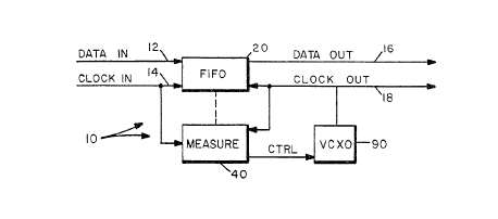
The desynchronization apparatus of the invention 10 for
generating ari ungagped DS3 signal from the data component of a
gapped STS-1 payload signal is seen generally in Fig. 2. The
desynchronization apparatus includes a FIFO means 20, a
measuring circuit 40, and a voltage controlled crystal
oscillator 90. The FIFO means 20 receives the data component
of the STS-2 payload signal (i.e. data In 12) according to a
gapped clock signal "clock In" 14 generated by a demultiplexer
(not shown) of a preprocessing block (not shown). The clock
In signal 14 as measured by its pulse width is typically 51.84
MHz + 20 ppm. However, the average rate of the clock In
signal is actually only 44.736 + 20 ppm due to the fact that
there are large gaps in the signal.
Data is preferably taken from the~FIFO 20 (at data Out
16) at the same rate at which it is received, and it is the
function of the desynchronization apparatus l0 to generate a
clock Out signal 18 which matches the average rate of the data
SUBSTITUTE SHEET
Wp 92/08304 FCT/US91/08208
6
In signal 12 with a minimum of fitter. For purposes herein,
fitter is defined as the variation in the 'time of occurrence
of an individual clock edge of a clock with respect to the
average time of occurrence of the clock edge of that clock.
In order to generate an appropriate, clock Out signal 18,
the clock In signal 14 and clock Out signal 18 are fed to the
measuring circuit 40. As will be described in more detail
hereinafter with reference to Fig. 3, the measuring circuit
makes a comparison of indications related to the clock In and
clock Out signals to effectively determine whether FIFO 20 is
filling up with data, or is being depleted of data. As a
result of the comparison, the measuring circuit 40 provides a
control signal to the VCXO 90 which helps control the VCXO
clock output.
Turning to Fig. 3, a more detailed block diagram is seen
of the preferred apparatus 20 of the invention. As indicated
in Fig. 3, the FIFO means 20 is implemented with a "write
side" serial to parallel converter 23, a "write side" three
bit counter 27 (shown in phantom because it can be replaced by
a signal from the nine bit binary counter 44 as discussed
below), a "write side" address generator 29, a thirty-two byte
RAM 30, and a "read side" parallel to serial converter 33, a
"read side" three bit counter 37 (shown in phantom because it
can be replaced by a signal from the nine bit binary counter
48 as discussed below), and a "read side" address generator
39. The measuring circuit 40 is implemented with the nine bit
write counter 44, the nine bit binary read counter 48, an
exclusive OR (XOR) gate 52, and a low pass filter 56.
SUBSTITUTE SHEET
WO 92/08304 c, "~ s~ , PCTlUS91>08208
7
Looking first at the FIFO means 20, a data In signal 12,
and clock In and write enable signals 14a and l4b are received
by the serial/parallel converter 23 from a preprocessing block
(not shown). The write enable signal indicates when the data
signal being received is the data component of the STS-1
payload. Thus, the write enable signal 14b effectively gaps
the clock In signal 14a, and the data accepted by the
serial/parallel converter is the gapped data component of the
STS-1 payload.
The serial/parallel converter receives the bit serial
stream of data, and provides therefrom eight bit bytes of data
which are sent for storage in the byte RAM 30. As the bits
are received by the serial/parallel converter, a three bit
counter 27 counts the bits (or gapped clock cycles), and sends
a control signal to the address generator 29 every time eight
bits have been oounted; i.e. when a byte of data is available.
The address generator 29 is preferably a recirculating
thirty-two bit shift buffer having a single one value, with
the remainder zeros. When the control signal from the three
bit counter 27 is received by the address generator 29, the
address generator 29 shifts its values. As a result, the next
byte location in the thirty-two byte RAM 30 is enabled, and
the eight bit byte of data is written to the enabled location.
The read side of the FIFO circuit 20 essentially
parallels the write side, except that the read side
parallel/serial converter 33 receives the output clock 18 as
its input, and the read side three bit counter 37 counts eight
output clock cycles in generating a control signal for the
read side address generator 39. Address generator 39 is also
a thirty-two bit shift register which is preferably
initialized with its "1" value sixteen bits away from the "1"
~Talue location in address generator 29; i.e, the first byte of
data read from byte RAM 30 is taken from a location sixteen
SUBSTETUTE SHEE'~
WO 92/08304 ~ ~ ~ PCT/L'S91/08208
G7 ~ tJ .J
bytes away in byte RAM 30 from where the first byte of data is
written. By separating the read and write addresses in this
manner, the byte RAM 30 provides enough buffer for
desynchronizing the evenly clocked outgoing DS3 signal from
the gapped data component of the STS-1 signal,
As aforementioned, the measuring circuit 40 makes a
comparison of indications related to the clock In and clock
Out signals to,effectively determine whether the FIFO means 20
(i.e. the byte RAM 30) is filling up with data, or is being
depleted of data. The measuring circuit accomplishes its
determination by feeding the gapped clock In signal to
counter 44, the output clock signal to counter 48, feeding the
msb of each counter into an XOR gate 52 and low pass filtering
the output of the XOR gate 52 with the low pass filter 56. In
particular, the write enable and clock In signals 14a and 14b
are used as inputs to counter 44 which effectively counts
cycles of a gapped write cloak. Counter 44 is preferably a
nine bit binary counter, although a different size counter.
could be utilized depending upon how quickly changes in output
clock rates are desired. With a nine bit binary counter,
eight bits relate to all bit locations in the thirty-two byte
RAM 30; three bits for eacr. byte, and five bits to specify a
particular byte. Thus, the change of the ninth bit indicates
that the address generator 29 has gone through an entire
cycle; i.e. the byte RAM has been completely rewritten with
data. Also, the change of the fourth bit indicates that an
entire byte has been received. Thus, as seen in phantom in
Fig. 3, the fourth bit (or the first three bits together) may
be used as the shift control for the address generator 29
instead of three bit counter 27.
The output clock signal 18 is similarly fed to a nine bit
binary counter 48 which indicates that the address generator
39 has gone through an entire cycle (i.e. thirty-two bytes
SUBSTI T UTE SHFET
WO 92108304 ~, ~.'~ ,~ , PCT/US91/08208
~~~~:~i~~
9
have been read out of the byte RAM), and which may also be
used, as shown in phantom, to replace the three bit counter
37. By taking the msb's of each of counters 44 and 48, and
feeding them as inputs into the XOR gate 52, the XOR gate will
provide a signal whose duty cycle relates to the relative
speeds at which the byte RAM is being filled and emptied. Far
example, if the address generator pointers are initialized to
be sixteen bytes.apart, and they stay sixteen bytes apart, the
output of XOR gate will be a signal which half the time is at
the value one, and half the time is at a value zero. Thus,
the duty cycle of the XOR output signal is fifty percent.
However, if data is fed into the byte RAM faster than it is
taken out, the duty cycle will increase, as the time during
which the msb's are a different value will increase. The time
during which the msb's are a different value will increase
because the change of the msb of the write counter 44 will
occur earlier than before, while the change of the msb of the
read counter 48 will occur at the same time. Conversely, if
the data taken out of the byte RAM is taken out faster than
data is being fed into the byte RAM, the duty cycle of the XOR
output signal will decrease.
Because the data component of the STS-1 payload is a
severely gapped signal, it will be appreciated by those
skilled in the art that the duty cycle of particular outputs
from the XOR gate will vary significantly in both directions.
In order to eliminate the effect of these high frequency
disturbances, the output from the XOR gate is fed through a
low pass filter 56 which is preferably comprised of a lOK ,
resistor and a .1 microfarad capacitor. The low pass filter
56 effectively averages the duty cycle of the output of the
XOR gate over a long period of time (in relative terms
compared to the high rate signals being received and
regeneratedj. The output of the low pass filter is a voltage
signal which varies slightly in response to slow changes in
the duty cycle of the XOR gate output; i.e. in response to the
SU~STITUT~ S~f FET
WO 92!08304 PCf/US91/08208
C t I.
,f ~ ;~ 3 '
~) ~~ GF~ "11 IFl'
do compont of the duty cycle. For example, for a five volt
system, a long term fifty percent duty cycle signal would
produce a 2.5V (2.5V = (50%)5V) output. For a long term
fifty-one percent duty cycle (the signal is high 51% of the
time), the output voltage would be 2.55V (2.55V = (51%)5V).
The output voltage signal from the low pass filter is fed to
the VCXO which changes its clock output only slightly in
response to such a change in voltage. The change in output
frequency depends on the change in voltage, and the gain
constant of the VCXO. Preferred gain constants are between 50
and 150 ppm per volt. Thus, for a VCXO having a gain constant
of I00 ppm per volt, and producing a nominal frequency of
44.736 MHz, the long term change in the do component of the
duty cycle from fifty to fifty-one percent (which would be an
extraordinarily large change as discussed below) would result
in a frequency change of approximately 224 Hz: 44.736 MHz x
100 ppm x .05V.
When the rate of the output clock is increased or
decreased in response to the voltage signal sent by the low
pass filter 56 to the VCXO 90, the data is taken from the byte
RAM 30 accordingly, and the rate at which the nine bit counter
48 counts is also changed accordingly. Thus, a feedback loop
is generated, which tends to force the duty cycle of the XOR
gate 52 to an equilibrium; e.g. fifty percent. Similarly, the
depth of the FIFO,~i.e., the number of bytes in RAM 30, is
forced toward being, sixteen bytes, i.e. fifty percent full.
It should be appreciated that the equilibrium point of
the duty cycle of the XOR gate signal can be changed, e.g., by
changing the voltage offsets in the loop, and need not be
fifty percent. For example, it might take 2.8V instead of
2.5V for the VCXO to output the 44.736 MHz nominal rate. In
that case, in order to maintain equilibrium, the equilibrium
of the system will be maintained with the fullness of the FIFO
SUSST~TUTE SHEEN
WO 92/08304 ~ ~ ~ ~ J ~J ~ PCT/US91/08208
m
at other than fifty percent. Similarly, the voltages of the
system might change while running without a change in data
rates. In that situation, if for example, the voltage to the
VCXO is increased, at first the VCXO increases its output
clock rate. However, since the input data rate had not
increased, the increase in the output clock rate will cause a
decrease in duty cycle as data will be read from the FIFO
faster than it is being placed in the FIFO. With a decreased
duty cycle, the voltage to the VCXO is decreased until
equilibrium is reached at a lower duty cycle and a less filled
FIFO.
It should also be appreciated that by providing large
capacity binary counters, by filtering the output signal of
the XOR gate to eliminate high frequency changes, and by using
a VCXO which is relatively insensitive to voltage changes, a
stable system which meets Standards requirements is provided.
The large capacity binary counters guarantee that when the
gagged data input has one more or one fewer bit over a
particular time interval, the duty cycle will not change
dramatically. For example, with nine bit binary counters
preferably tracking a thirty-two byte RAM, the duty cycle will
change by approximately four tenths of one percent (50 - 50 to
50.4 - 49.6j in response to a one bit change over the thirty-
two bytes. While, because of the large gaps in the incoming
signal, the duty cycle might swing tens of percent in one way
or the other in the very short term, these high frequency
changes are filtered out by the low pass filter, and only
changes over a relatively long period of time will affect the
output~clock rate. Over the long term, large changes in clock
rates are not. permitted according to Standards, and therefore,
a do duty cycle change of even one percent would be extremely
large. Further, by using an insensitive VCXO, only a very
small output clock change is generated in response to the
voltage change.
SUSST~ThTE SHEE i~
WO 92/08304 ~ ~ (~ ). ~ PC'f/1JS91/08208
12
Turning to Figure 4, an alternative embadiment of the
invention is shown. In Figure 4, an apparatus 100 is provided
with a FIFO means 120 which includes a one bit wide, two
hundred fifty-six bit long RAM 130, and two address generators
129 and 139. The address generators 129 and 139 are
preferably two hundred fifty-six bit long shift registers with
a single one value. The measuring circuit 140 is identical to
the measuring circuit 40 of Fig. 3 and includes two nine bit
counters 144 and 148, and XOR gate 152, and a low pass filter
156. The output of the LPF 156 is sent to a VCXO 90 which
provides the output clock which is fed back to the nine bit
binary counter 148.
The primary differences between the apparatus of Fig. 4
and that of Fig. 3, is that the data is fed into RRM 130 in a
bit serial fashion which obviates the need for the
serial/parallel and parallel/serial converters as well as the
three bit counters, and that the location in RAM 130 into
which the bits are fed is dictated by the eight least
significant bits (lsb's) of the binary counters 144 and 148.
However, by requiring that data is fed into the RAM 130 one
bit at a time, an extremely fast circuit is required, making
implementation more difficult and expensive.
There has been described and illustrated herein apparatus
for generating an ungapped DS3 signal from the data component
of a gapped STS-1 payload signal. While particular
embodiments of the invention have been described, it is not
intended that the invention be limited thereby, as it is
intended that the invention be broad in scope and that the
specifications be read likewise. Thus, while byte and bit
wide RAMs were described for use as FIFO means, it will be
appreciated that other types of FIFOs such as a bit serial -
asynchronous FIFO could be used. In fact, regardless of the
type of FIFO means utilized, shift register address generators
SUBSTITUTE SHEE T
WO 92/08304 O ~ PCT/L'S9l/08208
2~~3~rd~
13
are not required, and could be replaced with binary counters.
Also, while an XOR gate for comparing the msb's of two binary
counters was described for providing an indication of the
fullness of the FIFO means, it will be appreciated that other
measuring means could be utilized. For example, a comparator
for comparing (subtracting) the counts of the counters could
be utilized to provide an indication of fullness. Or, a
comparator for comparing the address locations provided by the
address generators could be utilized. It should be realized,
however, that. such comparators do not provide as desirable a
measurement as the measurement obtained by the binary counters
and XOR gate (which is filtered by the filter), as the
measurement-obtained with the comparator is typically both
quantized in time and in amplitude. With the preferred means
for measuring fullness of the FIFO, there is no amplitude
quantization, as the binary counters are asynchronous, and the
XOR gate provides a signal with a duty cycle which is not
stepped. Also, because the measurement is continuous (due to
asynchronous binary counters), the measurement is not
quantized in time.
It will further be appreciated by those skilled in the
art that while certain size RAMs and counters were described,
and while values for the components of the low pass filter
'were provided, components of different sizes and values could
be utilized effectively to tailor the circuit to desired
parameters. In fact, different types of low pass filters
could be utilized. Therefore, it will be apparent to those
skilled in the art that other changes and modifications may be
made to the invention as described in the specification
without departing from the spirit and scope of the invention.
SUSST1TUTE SHEET