Some of the information on this Web page has been provided by external sources. The Government of Canada is not responsible for the accuracy, reliability or currency of the information supplied by external sources. Users wishing to rely upon this information should consult directly with the source of the information. Content provided by external sources is not subject to official languages, privacy and accessibility requirements.
Any discrepancies in the text and image of the Claims and Abstract are due to differing posting times. Text of the Claims and Abstract are posted:
| (12) Patent: | (11) CA 2095350 |
|---|---|
| (54) English Title: | PHASE LOCKING CIRCUIT FOR JITTER REDUCTION IN A DIGITAL MULTIPLEX SYSTEM |
| (54) French Title: | CIRCUIT DE VERROUILLAGE DE PHASE POUR REDUIRE LE SAUTILLEMENT DANS UN SYSTEME DE COMMUTATION MULTIPLEX NUMERIQUE |
| Status: | Deemed expired |
| (51) International Patent Classification (IPC): |
|
|---|---|
| (72) Inventors : |
|
| (73) Owners : |
|
| (71) Applicants : | |
| (74) Agent: | MARKS & CLERK |
| (74) Associate agent: | |
| (45) Issued: | 1999-02-02 |
| (86) PCT Filing Date: | 1991-07-09 |
| (87) Open to Public Inspection: | 1992-01-11 |
| Examination requested: | 1993-09-21 |
| Availability of licence: | N/A |
| (25) Language of filing: | English |
| Patent Cooperation Treaty (PCT): | Yes |
|---|---|
| (86) PCT Filing Number: | PCT/SE1991/000487 |
| (87) International Publication Number: | WO1992/001344 |
| (85) National Entry: | 1993-04-30 |
| (30) Application Priority Data: | ||||||
|---|---|---|---|---|---|---|
|
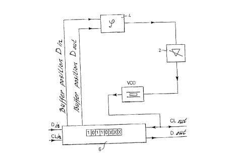
A phase-locking circuit for jitter reduction in a
digital multiplex system includes a feed-back operational
amplifier having two inputs. Two anti-parallel coupled
diodes are arranged at one input of the operational
amplifier for achieving automatic gain control. The other
input of the operational amplifier is connected to a
reference voltage. The operational amplifier is of the FET
or CMOS type, having high-ohmic amplifier inputs.
Circuit de verrouillage de phase permettant de réduire la gigue dans un système multiplex numérique. Comprend un amplificateur opérationnel à réaction, à deux entrées. Deux diodes sont montées tête-bêche à une entrée de l'amplificateur opérationnel aux fins de la commande de gain automatique. L'autre entrée de l'amplificateur opérationnel est connectée à une source de tension de référence. L'amplificateur opérationnel est de type FET ou CMOS, à entrées à haute valeur ohmique.
Note: Claims are shown in the official language in which they were submitted.
Note: Descriptions are shown in the official language in which they were submitted.
For a clearer understanding of the status of the application/patent presented on this page, the site Disclaimer , as well as the definitions for Patent , Administrative Status , Maintenance Fee and Payment History should be consulted.
| Title | Date |
|---|---|
| Forecasted Issue Date | 1999-02-02 |
| (86) PCT Filing Date | 1991-07-09 |
| (87) PCT Publication Date | 1992-01-11 |
| (85) National Entry | 1993-04-30 |
| Examination Requested | 1993-09-21 |
| (45) Issued | 1999-02-02 |
| Deemed Expired | 2000-07-10 |
There is no abandonment history.
| Fee Type | Anniversary Year | Due Date | Amount Paid | Paid Date |
|---|---|---|---|---|
| Application Fee | $0.00 | 1993-04-30 | ||
| Maintenance Fee - Application - New Act | 2 | 1993-07-09 | $100.00 | 1993-06-30 |
| Registration of a document - section 124 | $0.00 | 1993-10-19 | ||
| Maintenance Fee - Application - New Act | 3 | 1994-07-11 | $100.00 | 1994-06-28 |
| Maintenance Fee - Application - New Act | 4 | 1995-07-10 | $100.00 | 1995-06-28 |
| Maintenance Fee - Application - New Act | 5 | 1996-07-09 | $150.00 | 1996-07-02 |
| Maintenance Fee - Application - New Act | 6 | 1997-07-09 | $150.00 | 1997-06-26 |
| Maintenance Fee - Application - New Act | 7 | 1998-07-09 | $150.00 | 1998-06-30 |
| Final Fee | $300.00 | 1998-10-05 |
Note: Records showing the ownership history in alphabetical order.
| Current Owners on Record |
|---|
| TELEFONAKTIEBOLAGET LM ERICSSON |
| Past Owners on Record |
|---|
| BLADH, MATS |

