Note: Descriptions are shown in the official language in which they were submitted.
2095514 ~ 1
Description
Digital 8witching 8ystem Interconnecting
Buses With Incompatible Protocols
TBCHNICAL FIELD
The present invention relates to systems for
connecting buses of information systems having
incompatible protocols.
R~C~R~UND ART
Digital switching systems have been developed which
provide non-blocking digital switching in which pulse
code modulation is used to digitize information such as
voice channels to permit controllable switching of
information on the inputs to the outputs of the digital
switch. For example a total of 32 voice channels may be
pulse code modulated and time division multiplexed so
that selected channels on the inputs of the digital
switch are connected to different outputs of the digital
switch. The switching required to produce the time
division multiplexed switching of different channels
between selected inputs and outputs is produced by
control switching signals applied to the digital switches
of the switching matrix.
In the field of telephony numerous manufacturers
make voice digitizing boards which convert individual
channels (conversation) into a time division multiplexed
PCM encoded format in which multiple bits encode
respective samples of each channel. On a wire pair
typically 24 or 32 different channels are encoded by
assigning individual channels representative of a
conversation to a particular time slot within a frame of
2095 514 ~
the time division multiplexed PCM encoded information.
Switching of the PCM information on a bus is controlled
by a digital switch which permits the selective
connection of individual channels through the public
switched telephone network to particular telephone lines.
The voice digitizing products of manufacturers such
as Dialogic Corporation, Natural Microsystems
Corporation, Rhetorex and the assignee of the present
invention, American Tel-A-Systems, Inc. have incompatible
bus protocols which prevent direct interconnecting of
buses of systems made by these manufacturers. The buses
utilized by the aforementioned manufacturers and others
have several possible clock rates such as 1.544 MHz,
2.048 MHz, 4.096 MHz and different 8 kHz synchronization
of the frame rate as provided respectively by
specifications of integrated circuits manufactured by
National Semiconductor or Mitel Corporation and further
synchronization signals which define superframes utilized
for Tl service which are a combination of multiples of 6
basic frames at the 8 kHz frame rate. As a result of the
diversity of the clock rates, synchronization and other
timing signals utilized by the various manufacturers
there is no compatible bus protocol for interconnecting
information systems which have been made by the
interconnection of boards provided by a particular
manufacturer with an information system made by
interconnecting boards from another manufacturer. As a
result a user of a system having digitized voice to date
is required to make difficult choices as to which
manufacturers' products to purchase which limit the
overall functional capability of a system and the ability
to modify the system in the future as a consequence of
2 0 9 5 5 1 4 .
the inability to interconnect subsystems formed from
products manufactured by different manufacturers.
Circuit boards are marketed which may be inserted
into the expansion slot of a standard PC such as a PC-AT
to control different types of analog telephone ports.
These boards provide analog telephone line port
receptacles for connection to the public switched
telephone network (PSTN). The analog ports may be for a
station port which supplies battery feed capable of
applying ring voltage to a line along with normal line
status and control functions for the purpose of
interfacing two telephones; a loop start port of the so-
called "plain old telephone service" which includes all
normal line status monitoring; a ground start port which
provides a ground start line interface; a DID port which
provides all known RS-464 and IEEE standard DID protocols
including wink, immediate start as well as DTMF and pulse
dialing; an E & M port which may be configured for type
I or II signalling and a battery feed port which provides
battery but cannot provide ring voltage. These circuit
boards have programmable jumpers or switches which permit
each of the ports of the circuit to be programmed to have
the desired type of line characteristic. The
disadvantage of this type of circuit board is that all of
the circuits necessary for supporting the types of
possible line interfaces which may be provided must be
present on the board even though the customer may only
want to use a fraction of the overall number of line type
interfaces that are supported by the board. As a result,
the expense of the circuit board is increased and further
the number of analog lines which may be connected to the
board is lessened as a consequence of the necessary
2 0 9 5 5 1 4
electronics for supporting all of the lines taking up
space which lessens the number of ports which may be on
the board.
Another design of a circuit board for interfacing a
PC with analog lines does not permit the programming of
the characteristic of the line to which the circuit board
is to be connected. Each circuit board of this type is
hard-wired to support one or more types of analog line
interfaces. As a result, this product is not
programmable and may be only used for specific
applications for specific connections to analog lines
which prevents it from being reconfigured by the
customers to interface with different types of analog
lines.
DI8CLOSURE OF THB INVENTION
The present invention is a digital switching system
utilizing a digital switching matrix and further an
information system having a plurality of connected
information buses of different information systems which
each have individual bus protocols which are incompatible
and different from the protocols of the other buses of
the remaining information systems that prevents
communications directly between buses of the information
systems. A host processor is coupled to each of the
plurality of information systems for controlling the
information systems with commands causing at least one of
the information systems to transmit and at least one of
the information systems to receive information by
connecting the information bus of the transmitting and
the information bus of the receiving information systems
with a digital switching matrix. A control processor
2 0 9 5 5 1 4
controls the digital switching matrix by generating
control signals controlling switching of the switches of
the digital switching matrix in response to commands from
the host processor. The invention is particularly
applicable to the interconnection of telephony systems
having incompatible information buses transmitting
information in the form of time division multiplexed PCM
encoded digitized voice or data which are made from
products of different manufacturers having different bus
specifications. Individual telephone conversations,
which are digitized by using time division multiplexed
PCM encoding to produce multiple channels on pairs of
conductors of the bus of the system, may be connected to
other pairs of conductors on the bus within one of the
connected information systems or to another information
system through the switching matrix by suitable
programming of the information systems and the control
processor.
Control circuitry is provided, which is responsive
to the control processor, for providing a master clock
signal to the information systems which controls a rate
of information transmission and reception on the buses by
the information systems and further the generation of
master synchronization signals for controlling framing
and other master timing signals which are transmitted to
the information systems to provide compatible systems
clock, synchronization and control signals. The commands
from the host processor control the generation of the
master clock with the host processor commanding the
information systems to control the transmission and
reception on the information buses under the control of
the master clock. The master clock may be synchronized
2095 514 .
to generate the clock signal with another signal provided
on one of the information buses of the information
systems to the control circuitry such as, but not limited
to, a timing specification provided by the PSTN such as
where Tl service is provided. Additionally, the control
circuitry also provides the synchronization signals to
the information systems which synchronize frames of
information transmitted and received on the buses by the
information systems.
In a preferred application of the present invention
the host processor is a PC and the control processor is
commanded by the host processor to perform the necessary
switching interconnections of the switching matrix in
order to ensure that appropriate connections are made
between the buses of the information systems which are
connected to the switching matrix which result in the
transmission and reception of information as commanded by
the host processor to the information systems as a
consequence of the commands issued from the host
processor to the information systems. As a result of the
commands controlling the connection of the buses from the
incompatible information systems through the switching
matrix and the generation of a master clock signal
controlling the rate of transmission of information on
the buses as well as synchronization signals, the
information systems individually which have incompatible
bus specifications are made compatible by the supplying
of common clock and synchronization information to all
systems. This ensures the compatibility of information
transmission on and between the buses of the information
systems and the appropriate signal paths through the
switching matrix being established between the buses as
2095 5 14
a consequence of the switching of the switching matrix
being under the control of the commands issued by the
host processor.
The invention provides distinct advantages over the
prior art which does not permit incompatible information
systems to be interconnected through their buses as a
consequence of incompatible bus protocols. As a result,
digitized voice and other forms of digitized information,
such as ISDN, may be transmitted between incompatible
digital information systems by the supplying of
appropriate commands from a host processor such as a PC
to the control processor which controls the generation of
centralized clock and synchronization information which
is transmitted to the individual information systems to
provide their clock and synchronization signals. As a
result of using a conventional PC and a processor such as
a microprocessor, which is part of a circuit board that
is connected to the PC as a peripheral device which is
controlled by the PC to control the digital switching
matrix and the control circuitry to generate the common
system timing, the overall cost of the system is reduced
while permitting the interconnection of otherwise
incompatible information systems in conventional usage in
applications such as telephony where digitized voice
products are provided by diverse manufacturers of voice
digitizing circuit boards used in combination with
digital switches to provide diverse telephonic services
through customers connected to the PSTN.
The invention further provides a line interface
between the PSTN, a personal computer and an information
bus which permits the control by a personal computer of
the interfacing of multiple types of analog telephone
2095 5 14
lines with the PSTN. Individual modules are inserted
into slots which configure an interface with a particular
type of analog telephone line. As a consequence of the
module containing circuitry unique to the type(s) of
analog line interface created by its insertion in the
appropriate slot of the circuit board, the circuit board
contains less circuitry than the prior art as a result of
specialized circuits for producing the interface with a
particular type of analog line being contained in the
module as contrasted with the circuit board as in the
prior art. Furthermore additional ports for driving
additional analog lines are provided as a consequence of
the circuit board containing less circuitry than the
prior art as a consequence of particular circuitry for
configuring a particular type of analog line interface
being present within the module which is inserted into
the slot of the circuit board. The line interface may be
configured by the insertion of the appropriate module to
provide an interface with any combination of DID, E & M,
source, ground start, loop start or battery feed type
analog lines. The line interface provides the low level
protocols and signalling necessary for the different line
types. Moreover, an interface with a bus is provided for
access to other interface boards. A host processor,
which may be a PC, controls the control processor of the
line interface by suitable commands which are transmitted
from the host processor to the control processor.
A digital switching system in accordance with the
invention includes a digital switching matrix having an
input bus and an output bus with information on the input
bus being selectively connectable to information on the
output bus in response to control signals applied to
2095 5 14
switches of the switching matrix; a plurality of
information systems with each information system having
an information bus for transmitting and receiving
information using a protocol which is different from a
protocol used by the information bus of each of the other
information systems with conductors of the information
buses of the information systems being electrically
connected to the input and output buses of the matrix to
permit information transmitted from a conductor of any of
the information buses to be received by another conductor
of any of the information buses through the information
bus, the switching matrix and the output bus; a host
processor, coupled to each of the plurality of
information systems, for controlling the information
systems with commands causing at least one of the
information systems to transmit and at least one of the
information systems to receive information using the
information bus of the transmitting and the information
bus of the receiving information systems, the switching
matrix and the input and output buses; and a control
processor, responsive to commands from the host
processor, for generating the control signals controlling
switching of the switches of the digital switching
matrix. Information transmitted and received on the
information buses may be encoded in a time division
multiplexed pulse code modulated format to provide a
plurality of channels of information with each channel
being time division multiplexed. The channels of
information may contain audio voice information or data.
At least one of the systems may be connected to a public
switched telephone network and the network may provide a
timing reference to the switching system used to generate
2095 51 4
a master clock signal by control circuitry to control a
rate of transmission and reception on the buses by the
information systems. The host processor also transmits
commands to a plurality of the information systems and to
S the control processor to cause information to be
transmitted from the bus of one of the information
systems through the digital switching matrix for receipt
by the bus of another one of the information systems.
The host processor transmits commands to one of the
information systems and to the control processor to cause
information to be transmitted and received by the bus of
the information system receiving the command through the
switching matrix. The host processor also transmits
commands to at least one of the information systems and
to the control processor to cause a plurality of channels
of information to be transmitted from at least one bus of
one of the information systems through the switching
matrix to at least one bus of at least one of the
information systems. The host processor also transmits
commands to a plurality of the information systems and to
the control processor to cause the plurality of channels
of information to be transmitted from at least one
information bus of one of the information systems through
the switching matrix to at least one information bus of
another of the information systems. Finally, the host
processor transmits commands to a plurality of
information systems and to the control processor to cause
full duplex communications between buses of at least two
of the information systems through the switching matrix.
The invention further includes control circuitry,
responsive to the control processor, for providing a
master clock signal to the information systems which
.
2 0 9 5 5 1 4 3
11
controls a rate of information transmission and reception on
the buses by the information systems. The commands control the
generation of the master clock with the host processor
commanding the information systems to control the transmission
and reception on the information buses under the control of
the master clock. The master clock may be synchronized to
generate the clock signal with another signal provided on one
of the information buses of the information systems. The
control circuitry also provides synchronization signals to the
information systems which synchronize frames of information
transmitted and received on the buses by the information
systems. The commands control the generation of the synchron-
ization signals with the host processor commanding the inform-
ation systems to synchronize the transmission and reception of
frames of information on the information buses under the
control of the synchronization signals.
A system in accordance with the invention includes a
plurality of information systems with each information system
having an information bus for transmitting and receiving
information using a protocol which is different from a proto-
col used by the information bus of each of the other inform-
ation systems with conductors of the information buses of the
information systems being electrically connected in response
to control signals to permit information transmitted on a
conductor of any of the information buses to be received by
another conductor of any of the information buses; a host
processor, coupled to each of the plurality of the information
systems, for controlling the information systems with commands
causing at least one of the information systems to transmit
and at least one of the information systems to receive inform-
ation using the information bus of the transmitting and the
~i
71812-2
-
2 0 9 5 5 1 4
12
information bus of the receiving information systems; a
control processor, responsive to commands from the host
processor, for generating the control signals; and control
circuitry, responsive to the control processor, for providing
a master clock signal to the information systems which
controls a rate of information transmission and reception on
the buses by the information systems. The commands control the
generation of the master clock with the host processor
commanding the information systems to control the transmission
and reception of information on the information buses under
the control of the master clock. The master clock may be
synchronized to generate the clock signal with another signal
provided on one of the information buses of the information
systems. The control circuitry also provides synchronization
signals to the information systems which synchronize frames of
information transmitted and received on the buses by the
information systems. The commands control the generation of
the synchronization signals with the host processor commanding
the information systems to synchronize the transmission and
reception of frames on the information buses under the control
of the synchronization signals. Information transmitted and
received on the information buses may be encoded in a pulse
code modulation format to provide a plurality of channels of
information with each channel being time division multiplexed.
The channels of information may contain audio voice inform-
ation. At least one of the information systems may be
connected to a public switched telephone network and the
network may provide a timing reference to the system used to
generate the master clock signal.
A system in accordance with the invention includes a
digital switching system comprising: a digital switching
,;y
71812-2
2095 5 14
13
matrix having an input bus and an output bus with information
on the input bus being selectively connectable to information
on the output bus in response to control signals applied to
switches of the switching matrix; a plurality of information
systems with each information system having an information bus
for transmitting and receiving information using a protocol
which is different from a protocol used by the information bus
of each of the other information systems with conductors of
the information buses of the information systems being
electrically connected to the input and the output buses of
the matrix to permit information transmitted on a conductor of
any of the information buses to be received by another
conductor of any of the information buses through the input
bus, the switching matrix and the output bus; and at least one
processor, coupled to each of the plurality of the information
systems, for controlling the information systems with commands
causing at least one of the information systems to transmit
and at least one of the information systems to receive
information using the information bus of the transmitting and
the information bus of the receiving information systems, the
switching matrix and the input and output buses, and for
generating the control signals controlling switching of the
switches of the digital switching matrix.
A system in accordance with the invention includes a
plurality of information systems with each information system
having an information bus for transmitting and receiving
information using a protocol which is different from a
protocol used by the information bus of each of the other
information systems with conductors of the information buses
of the information systems being electrically connected in
response to control signals to permit information transmitted
~'
71812-2
.... .... . ...
2095 5 14
13a
on a conductor of any of the information buses to be received
by another conductor of any of the information buses; at least
one processor, coupled to each of the plurality of the inform-
ation systems, for controlling the information systems with
commands causing at least one of the information systems to
transmit and at least one of the information systems to
receive information using the information bus of the trans-
mitting and the information bus of the receiving information
systems and for generating the control signals; and control
circuitry, responsive to the at least one processor, for
providing a master clock signal to the information systems
which controls a rate of information transmission and
reception on the buses by the information systems.
BRIEF DESCRIPTION OF THE DRAWINGS
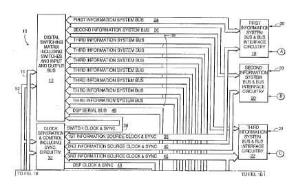
Figs. lA-lC illustrate a block diagram of a system
in accordance with the present invention.
Figs. 2 illustrate a block diagram of the clock
generation and control circuitry of Fig. 1.
Figs. 3A-3B illustrate a block diagram of a line
interface which may be utilized in the third information
system of Fig. 1.
Fig. 4 illustrates a block diagram of an E & M
module for use in the line interface of Fig. 3.
Fig. 5 illustrates a block diagram of a DID module
for use in the line interface of Fig. 3.
Fig. 6 illustrates a block diagram of a source
module for use in the line interface of Fig. 3.
Fig. 7 illustrates a ground start module for use in
the line interface of Fig. 3.
Fig. 8 illustrates a block diagram of a loop start
module for use in the line interface of Fig. 3.
~. ~
71812-2
~.~. .. ~ , . . . .
2095 5 14
13b
BEST MODE FOR CARRYING OUT THE INVENTION
Figs. lA-lC illustrate a block diagram of a digital
switching system 10 in accordance with the present invention.
A digital switching matrix, switches and input and output
buses 12 is the principal switching element of the digital
switching system. The input bus and the output bus is
conventional and is not separately illustrated. The digital
switching matrix functions such that information on the input
bus is selectively connectable to the information on the
output bus in
. . , . ~
~ ,~
~.
71812-2
14 2~955 14
response to control signals applied to the switches of
the switching matrix by control bus 14 which is connected
to a control processor 16 which is described in detail
below. A plurality of information systems, which are
respectively identified as first, second and third
information systems 18, 20 and 22, are connected to the
digital switching matrix, switches and input and output
buses 12 respectively by a first information system bus
24, second information system bus 26 and third
information system bus 28. It should be understood that
the present invention is not limited to the
interconnection of any particular number of information
systems and buses with the first, second and third
information systems 18, 20 and 22 and first, second and
third information system buses 24, 26 and 28 only being
representative of possible information systems and buses
which may be lesser or greater in number than the three
information systems and buses as illustrated. The first
information system 18 in a preferred embodiment of the
20 invention is representative of digital voice processing
circuitry manufactured by Dialogic Corporation. The
second information system 20 in a preferred embodiment of
the invention is representative of digital voice
processing circuitry manufactured by Natural
2 5 Microsystems. The third information system 22 in a
preferred embodiment of the invention is representative
of a group of interconnected line interface boards as
described in conjunction below in Figs. 3A, 3B and 4-8
which are manufactured by the assignee of the present
invention. Inputs 30 are representative of connections
between the PSTN and the configuration of circuits which
form a complete information system such as a telephony
2095 5 14
system comprised of interconnected circuit boards for
digital processing and switching of audio such as voice
communications or data for transmission by protocols such
as, but not limited to, ISDN. The digital switching
matrix, switches and input and output buses 12 may be
implemented by the connection of a plurality of Seimens
multi-point switching and conferencing integrated
circuits PEB 2245. Each integrated circuit of the
digital switching matrix, switches and input and output
buses 12 may switch any of 512 time and space division
multiplexed input channels to any of 256 time and space
division multiplexed output channels to provide PCM
encoding. The inputs are connected in parallel to form
a 512 channel by 512 channel switching matrix. Each
integrated circuit is capable of performing multiple
channel conferencing in which several input channels are
cross-connected and coupled to appropriate output
channels. The conferencing capability of the
aforementioned integrated circuits is limited to 64
inputs combined in a maximum of 21 conferences. It
should be understood that the present invention is not
limited to any particular configuration or operation of
the digital switching matrix, switches and input and
output buses 12. The first information system bus 24,
the second information system bus 26 and the third
information system bus 28 each have distinct, unique,
different and incompatible protocols which are
incompatible with the protocols of the other buses which
prevents direct connection of the buses into one system.
As a result, the buses 24, 26 and 28 may not be directly
connected to transfer information from one information
system 18, 20 and 22 to another information
2095 5 14
16
system relying upon the timing including clock signals
and synchronization signals generated by any one of the
information systems. The digital switching matrix,
switches and input and output buses 12 provide the
capability of connecting conductors of each of the
individual first information system bus 24, second
information system bus 26 and third information system
bus 28 to other conductors of that same bus or
alternatively to conductors of another one of the buses
and time division multiplexed information, such as voice
channels, from one bus 24, 26 and 28 to another bus. The
switching connections necessary to connect the input and
output buses of the information on the input bus to the
output bus of the digital switching matrix to provide
15 appropriate connections between conductors of a single
bus 24, 26 and 28 or between the buses is controlled by
the control signals applied on the control bus 14 by the
local processor 16.
The telephony industry has been characterized by
20 diverse products each developed to provide digital voice
processing utilizing time division multiplex PCM
encoding. However, the manufacturers of these products
have not developed a universal protocol which permits the
interconnection of systems each individually configured
25 with one manufacturer's products by bus interconnections
to systems configured with another manufacturer's
products. The present invention provides the capability
of interconnecting information systems through buses
which have incompatible protocols which have not been
designed to be interconnected. The digital switching
matrix, switches and input and output buses 12 provide
connections between the conductors of the buses 24, 26
2095 5 14
17
and 28 under the control of the control processor 16.
Clock generation and control circuitry 32, which is
controlled by the control processor 16, provides a master
clock signal to the information systems 18, 20 and 22
which controls a clock rate of information transmission
and reception of time division multiplexed PCM encoded
information on the buses 24, 26 and 28 by the information
systems and further controls the generation of necessary
synchronization signals which synchronize the
transmission and reception of frames of the time division
multiplexed PCM digitally encoded information produced by
the information systems on the information buses. In a
preferred embodiment where the first, second and third
information systems 18, 20 and 22 are respectively made
from circuits supplied by Dialogic, Natural Microsystems
and from the line interface circuits as described below
in conjunction with Figs. 3A, 3B and 4-8 of the assignee,
a 1.544 MHz, a 2.048 MHz clock signal and a 4.096 MHz
clock signal, an 8 kHz synchronization pulse marking the
beginning of frames conforming to National Semiconductor
timing specifications which may be used for information
systems made from circuits supplied by at least the
assignee, an 8 kHz synchronization pulse marking the
beginning of frames conforming to Mitel timing
specifications which may be used for an information
system configured from Natural Microsystems circuits and
synchronization signals which define a superframe used
for Tl service which marks multiples of 6 basic frames.
Additionally, the clock generation and control including
sync circuitry 32 may be synchronized to an external
timing reference from one of the information systems 18,
20 and 22 or from a source external to the information
-~ 2095 514
18
systems such as PSTN timing for T1 service used to
generate the master clock signal to control the clock
rate and timing of frames of information transmission and
reception on the buses by the information systems. In
this circumstance the master clock signal and
synchronization signals may be synchronized to any
external frame synchronization time reference. The
external timing reference is routed to the clock
generation and control including sync circuitry 32 by
control of the control processor 16. Removal of the
external clock reference causes the clock generation and
control including sync circuitry 32 to revert to
providing internally generated timing signals. Each of
the information systems 18, 20 and 22 may provide the
external timing reference through their connection to the
PSTN which results in the timing reference being fed to
the clock generation and control including sync circuitry
32 through the control processor 16 as described above.
In any event, the clock generation and control including
sync circuitry 32 supplies a common clock,
synchronization and any other timing signals to some or
all of the information systems 18, 20 and 22 either by
means of signals generated as a consequence of the
control of the control processor 16 as receiving commands
from the host processor 34 as described below which also
controls the switching connections produced by the
digital switching matrix, switches and input and output
buses 12 and the functioning of the first, second and
third information systems 18, 20 and 22 as operating to
transmit or receive information through the switching
matrix and input and output buses or from an external
source such as T1 timing.
2095 5 14
19
The host processor 34 is coupled to each of the
information systems 18, 20 and 22. The host processor 34
controls the information systems with commands causing at
least one of the information systems 18, 20 and 22 to
transmit and at least one of the information systems to
receive information using the information system buses
24, 26 or 28, the switching matrix, switches and input
and output buses 12. The different functions of the
system 10 which are controlled by the host processor 34
are specified by a command set inputted from the host
processor. The mnemonics of the command set are not
discussed herein and may be varied. The control
processor 16 is responsive to the commands issued from
the host processor 34, which may be a PC and preferably
may be PC-AT, for generating the control signals
outputted on the bus 14 to the digital switching matrix
of the digital switching matrix, switches and input and
output buses 12 for controlling the switching of the
switches in the switching matrix and the generation of
the clock signals and synchronization signals and any
other timing signals or control signals produced by the
clock generation and control including sync circuitry 32.
The clock generation and control including sync
circuitry 32 is connected to the digital switching
matrix, switches and input and output buses 12 by the
switch clock and sync bus 36. Similarly the clock
generation and control including sync circuitry 32
applies a common clock signal and synchronization signals
respectively to at least some and in many applications
all of the first, second and third information systems
18, 20 and 22 through the first information system clock
and sync bus 38, the second information system clock and
-
2095 5 14~ 20
sync bus 40 and the third information system clock and
sync bus 42. Finally, the clock generation and control
including sync circuitry 32 produces clock and sync
signals, which are applied through the DSP clock and sync
bus 44, to a plurality of digital signal processors 48 as
described below. A DSP serial bus 46 connects the
digital switching matrix, switches and input and output
buses 12 with the digital signal processors 48. The
information transmitted on the first, second and third
information system buses 24, 26 and 28 is preferably
encoded in time division multiplexed pulse code modulated
format to provide a plurality of channels of information
which may be for example twenty-four or thirty-two in
number without limitation with each channel being time
division multiplexed in frames. In a preferred
embodiment of the present invention, the PCM encoding of
information channels by time division multiplexing is
digitally encoded audio provided by the information
systems 18, 20 and 22 which are made from circuits
manufactured by manufacturers such as Dialogic, Natural
Microsystems and the assignee of the present invention as
described below. It should be understood that the
invention is not limited thereto and may for example
receive information in the form of data coming from the
PSTN in an ISDN format. The host processor 34 controls
both the local processor 16 and the first, second and
third information systems 18, 20 and 22 through commands.
The commands are decoded by the first, second and third
information systems 18, 20 and 22 to control which of the
information systems is transmitting information under
control provided by the clock generation and control
including sync circuitry 32 through the digital switching
-
2 0 9 5 5 1 4 21
matrix and input and output buses 12 to the receiving
information system. It should be understood that the
information systems 18, 20 and 22 may be connected
through the digital switching matrix, switches and input
and output buses 12 under the control of the control
processor 16 which in turn is controlled by the host
processor 34 for controlling the digital switching matrix
and input and output buses and the clock generation and
control including sync circuitry 32 to cause conductors
or information of one of the information system buses 24,
26 and 28 to be connected to other conductors or
information in the same information system bus so that
interconnects may be made in the same information system
or to cause conductors or information of one of the
information system buses to be connected to conductors or
information of another of the information system buses.
The aforementioned operation permits the interconnection
between information systems to provide interconnection of
buses which each have protocols which are incompatible
with the protocols of the buses of the other information
systems when operating within each of their respective
information systems with timing supplied internally to
the information system 18, 20 and 22 for controlling
information transfer on its information system bus 24, 26
and 28.
To perform the diverse foregoing functions, the host
processor 34 transmits commands to a plurality of the
information systems 18, 20 and 22 and to the control
processor 16 to cause information to be transmitted from
the information system bus 24, 26 or 28 of one of the
information systems 18, 20 or 22 through the digital
switching matrix, switches and input and output buses 12
2 0 9 5 5 1 4 ~ 22
for receipt by the bus of another one of the information
systems. Alternatively, the host processor 34 transmits
commands to one of the information systems 18, 20 and 22
and to the control processor 34 to cause information to
be transmitted and received by the bus of the information
system(s) receiving the command through the digital
switching matrix, switches and input and output buses 12.
Furthermore, the host processor 34 transmits commands to
at least one of the information systems 18, 20 and 22 and
lo to the control processor 16 to cause a plurality of
channels of information which are produced by the time
division multiplexed PCM encoding to encode each channel
in a multiple bit format such as 8 bits per channel to be
transmitted from at least one information system bus 24,
26 and 28 of the information systems through the digital
switching matrix, switches and input and output buses 12
to at least one bus of at least one of the information
systems. Moreover, the host processor 34 transmits
commands to a plurality of the information systems 18, 20
and 22 and to the control processor 16 to cause the
plurality of channels of information which are encoded in
the time division multiplexed PCM format to be
transmitted from at least one information system bus 24,
26 and 28 of one of the information systems 18, 20 and 22
through the digital switching matrix, switches and input
and output buses 12 to at least one information bus of
another of the information systems. Additionally, the
host processor 34 transmits commands to a plurality of
information systems 18, 20 and 22 and to the control
processor 16 to cause full duplex communications between
information system buses 24, 26 and 28 between buses of
at least two of the information systems through the
2 0 9 5 5 1 4 1 23
switching matrix. Duplex communications are achieved by
the setting of transmitting and receiving signal paths
from at least a pair of information systems 18, 20 and 22
through the digital switching matrix, switches and input
and output buses 12.
The clock generation and control including sync
circuitry 32 is responsive to the control processor 16 to
provide a master clock signal to the information systems
18, 20 and 22 which control a rate of information
transmission and reception on the information system
buses 24, 26 and 28 by the information systems. The
commands provided by the host processor 34 control the
generation of the master clock with the host processor
commanding the information systems 18, 20 and 22 to
control the transmission and reception of information on
the information system buses 24, 26 and 28 under the
control of the master clock. The master clock may be
synchronized from a timing reference from one of the
information systems 18, 20 and 22 or an external timing
reference not under the control of the host processor 34
such as that provided by Tl service through the
connection 30 to the PSTN. The clock generation and
control including sync circuitry 32 also provides the
synchronization signals which synchronize frames of the
time division multiplexed PCM encoded information
transmitted and received on the buses by the information
systems 18, 20 and 22. The commands from the host
processor 34 control the generation of the
synchronization signals with the host processor
commanding information systems 18, 20 and 22 to
synchronize the transmission and reception on the
information system buses 24, 26 and 28 under the control
2 0 9 5 5 t 4 ~
24
of the synchronization signals. A PC interface 50
interfaces the control processor 16 to the host
processor 34. Preferably the interface 50 is an ISA bus
interface which is in accordance with standards for a PC-
AT. The bus interface 50 supports shared interrupts anduses both the input/output and memory address spaces on
the host address bus and control 63 and the host data
bus 65 of the host processor 34. The bus interface 50
provides communications between the host processor 34 and
the control processor 16. Write-only input/output
locations are used in controlling interrupt generation
and memory base addresses. The input/output base address
is switch selectable in hexadecimal respectively at
input/output addresses between sequential hexadecimal
addresses 0200-0370 which jump in increments of 0010 in
hexadecimal address locations. Additional circuit boards
within the system 10 such as the third information
system 22 share interrupts mapped to the above-described
input/output addresses. The base input/output address is
used to reenable the interrupt control circuitry 61 that
generates interrupts 58 to the host processor 34 by the
host processor writing to the base input/output address
after each interrupt is serviced. The base memory
address for the dual ported ram 54 of the system 10 with
respect to the host processor 34 is set by the host
processor 34 writing to the base input/output address
plus 1. Data bits D0-D7 on the host data bus 65 map to
the address bits A15-A22 of the host address bus and
control 61 to set aside 32K address space for the
system 10. For example to map the dual ported RAM into
base address location D0000 in hexadecimal of the host
processor 34, data byte lA in hexadecimal would be
2 0 9 5 5 1 4 :' 25
written to the base input/output address plus 1. There
is no hardware to prevent mapping into memory below 640K.
On power-up the dual ported RAM 54 cannot be accessed by
the host processor 34. A jumper switch (not illustrated)
may be used to control the mapping of the dual ported
RAM 54 with respect to address bit A23 on the host
address bus and control 63. When this jumper switch is
installed, address bit A23 must be high to access the
board, in which case the board is mapped into memory
above 16M. The dual-ported RAM 54 may have 2K of memory
with the address for the system 10 being mapped into 32K
the base memory by the previously described input/output
strobe. The ISA bus interface (PC-AT) 50 may contain a
hex switch not illustrated to determine the 2K address
space within the 32K of base memory used by a particular
circuit board with the hex switch having hexadecimal
settings 0-F with each hexadecimal value representing a
multiple of 2K that is added to the base address of the
system as determined by the previously described
input/out strobe.
The shared interrupt allows the control processor 16
to generate an interrupt to the host processor 34 by
writing to the dual-ported RAM address 54 of 0000 in
hexadecimal. The interrupt is cleared when the host
processor 34 writes to location 0000 in hexadecimal and
also writes to the input/output base address. The host
processor 34 can generate an interrupt to the control
processor 16 by the writing of 0001 in hexadecimal into
the dual-ported RAM 54. The control processor 16 clears
the interrupt by writing to 0001 in hexadecimal.
Interrupt requests are generated by the interrupt control
circuitry 61 and are issued to the host processor 34 on
2 0 9 5 5 1 4 ~ 26
the interrupt lines 58 and are issued to the control
processor 16 on the interrupt line 59.
The system 10 supports the shared interrupts
provided in the PC-AT Technical Manual as follows: When
address 0 of the dual-ported RAM 54 is written into, an
interrupt is generated (edge-triggered). If more than
one circuit board such as other boards in a third
information system 22 attempts to generate the interrupt,
only one interrupt is actually generated. Furthermore,
if one board generates an interrupt and another board
tries to generate an interrupt before the first one is
serviced, the second interrupt will not occur until the
interrupt circuitry is rearmed. The interrupt service
routine must determine which board is interrupting.
After finding the appropriate board, it must perform all
software tasks required in servicing the interrupt. When
these tasks are completed the interrupt service routine
must write to location 0 of the dual ported RAM 54 to
enable the board to generate another interrupt. The last
step in the process is to write into the input/output
base address shared by all boards. This enables the
interrupt generating circuitry on all boards. If any
interrupts are pending (i.e. from a second board needing
service before the first board's interrupt service
routine is complete), another interrupt will be generated
at this time and the normal interrupt service routine
functions should be executed. This methodology allows
only one board to be serviced in a given interrupt
service routine. However, even if all of the boards in
the system 10 request an interrupt simultaneously, a
fresh interrupt is generated for each board until all
have been serviced. If desired, the interrupt service
2 0 9 5 5 1 4 27 2~i31~
routine can service all boards within one call to the
interrupt service routine. If this method is chosen, the
input/output strobe should not be generated until the
last board is serviced. This will prevent multiple
interrupts from occurring. The combination of the dual-
ported RAM 54 and the interrupt control circuitry 61
provides a complete communication mechanism which allows
the control processor 16 to send messages to the host
processor 34 and the host processor to send messages to
the control processor. These messages provide all the
control functions to a particular board to interface the
host processor 34 with a control processor 16.
The control processor 16 may be any suitable
microprocessor but an Hitachi 64180 may be utilized. The
control processor 16 provides access to the dual-ported
RAM 54, RAM 56 and ROM 60. In the aforementioned Hitachi
microprocessor a total of 64K of memory is provided. All
device specific functions are implemented via the
input/output interface of the control processor 16.
These communications include communications with the
digital signal processors 48, the clock generation and
control including circuitry 32, switching control of the
digital switching matrix, switches and input and output
buses 12 and serial input/output communications. The ROM
60 stores the application program. The RAM 56 is used
for variable storage and temporary information. The
dual-ported RAM 54 provides the interface to the host
processor 34 as described above. The control processor
16 controls all hardware specific aspects of the system.
For example, if a port in a circuit board of the third
information system 22 is to be connected to a port of
another board of the third information system, the
2 0 9 5 5 1 4 28
control processor 16 receives a command from the host
processor 34 to make this connection. The control
processor 16 translates the information into the
appropriate format and communicates with the digital
5 switching matrix, switches and input and output buses 12
via the appropriate input/output port. The control
processor 16 also controls the functions of the digital
signal processors 48 and determines the master clock
source for the system 10 such as for transmitting
lo information on the information system buses 24, 26 and 28
in time division multiplexed PCM format.
The bus 28 of the third information system bus and
bus interface circuitry 22 is designed to transfer time
division multiplexed PCM encoded information to and from
15 the boards within the hardware illustrated in Figs. 3-8
and to other peripherals. The interface includes an
appropriate master clock which may be 2.048 MHz but the
invention is not limited thereto, a transmit data signal,
a transmit synchronization signal, a receive data signal
20 and a receive synchronization signal. These signals are
provided on the information system bus 28 via a 10-pin
ribbon header. A plurality of third information systems
each of which is represented by an individual block 22
can be connected to the bus 28 to provide expansion. The
25 clock generation and control including sync circuitry 32
must provide the master clock and synchronization signals
to the third information system 22. As explained above
a time reference pulse such as a synchronization signal
representing the basic frame rate utilized for T1 service
30 may be provided through the PSTN interface 30 as used for
T1 service. The interface between the first information
system bus 24 and bus interface circuitry 18 is intended
2 0 9 5 5 1 4 29
in a preferred application to interface with Dialogic
Corporation products. In this circumstance it provides
a mechanism to transfer information between the digital
switching matrix, switches and input and output buses 12
5 and products which are connected to the information
system 18. It should be understood that the first
information system 18 is not limited to a particular bus
specification with regard to a particular manufacturer
such as Dialogic Corporation. The second information
system 20 and bus interface circuitry is intended in a
preferred application to interface with Natural
Microsystems products. It should be understood that the
invention is not limited thereto. In a preferred
embodiment up to 256 inputs and 256 outputs are coupled
15 to the second information system bus 26. Clock and
synchronization signals for the second information system
bus 26 may be generated by the second information system
bus and interface bus circuitry 20 or alternatively under
the control of the clock generation and control including
20 sync circuitry 32 when the host processor 34 is
controlling the transfer of information either within the
second information system 20 or between the second
information system 20 and the first and third information
systems 18 and 22. Finally, the clock source provided by
25 the second information system 20 may be used to
synchronize the clock generation and control including
sync circuitry 32 to slave the master clock signal for at
least one of the first and third information systems 18
and 22. In this case, the clock generation and control
30 including sync circuitry 32 acts as a master for the
first and third information systems 18 and 22 but is
slaved to the second information system 20. Any
2095514 30
information system may provide the clock source to the
clock generation and control including sync circuitry so
that the clock generation and control including sync
circuitry acts as a master for the remaining information
systems.
The digital signal processors 48 are used to provide
tone facilities to the system 10 and to boards within the
system that do not have built-in tone functions. The
digital signal processors 48 may be an Analog Devices
lo ADSP 2101. The digital signal processors 48 are not
required to operate the digital switching matrix,
switches and input and output buses 12 and provide
additional support for other functions of the overall
system not involving switching. For example the digital
signal processors 48 perform functions such as DTMF
generation and detection, call progress generation and
detection and MF generation and detection. The digital
signal processors 48 are connected to dual-ported RAM 62
via a DSP address and control bus 64 and a DSP data
bus 66. Furthermore the dual-ported RAM 62 is coupled to
the address bus and control 14 and the data bus 52 of the
control processor 16. The dual-ported RAM 62 is
configured into a first-in, first-out memory which stores
commands from the control processor 16 and information to
be transmitted to the processor such as acknowledgement
and indicating tones which have been detected.
A plurality of switches which are not illustrated
may be used to program functions in the system 10.
A switch may be used to provide a 2K offset in the 32K
address space of the system 10. A switch sets the
input/output base address. Another switch permits the
programming of interrupts for determining the interrupt
2 0 9 5 5 1 4 31
priority in the overall system. A switch may be used to
connect an interrupt pull-up resistor with only one
switch being installed on one board for a given
interrupt. If more than one board shares an interrupt
only one board will have this switch. Finally, a switch
may be connected to address location A23 of the address
bus and control 14 to permit access for memory above 16
megabytes.
Fig. 2 illustrates a block diagram of the clock
generation and control including sync circuitry 32 of
Fig. 1. Like reference numerals identify like parts in
Figs. 1 and 2. Clock generation circuitry 100, which may
be a Mitel integrated circuit MT8941, provides output
signals comprising clock signals of 1.544 MHz, 2.048 MHz,
4.096 MHz and an 8 kHz synchronization signal in response
to an input from a first oscillator 102 having a
frequency of 16.384 MHz and a second oscillator 104
having a frequency of 12.352 MHz. The foregoing outputs
are connected in parallel to clock translation circuitry
for the first information system 104, clock translation
circuitry for the second information system 106, clock
translation circuitry for the third information
system 108, switch clock translation circuitry 110 for
the digital switching matrix, switches and input and
output buses 12 and DSP clock translation circuitry 112
for the digital signal processors 48. It should be noted
that the communication paths between the clock generator
circuitry 110 and the first, second and third information
system clock translation circuitry 104, 106 and 108 are
illustrated as being bidirectional. However, in practice
the design of the information systems will determine if
communications are only in one direction from the clock
2 0 9 5 5 1 4 ~ 32
generator circuitry 100 or in two directions between the
clock generator circuitry and the information system
clock translation circuitry. When communications are
bidirectional, the information system is functioning as
a master clock with the clock generator circuitry being
slaved to the master information system and remaining
information systems being slaved to the clock generator
circuitry. The function of the translation circuitry
104, 106, 108, 110 and 112 is to vary pulse length and to
provide time shifting and inversion of the signals
generated by generator 100 to provide clock and sync
signals having the particular format for driving the
buses 24, 26 and 28, the switching matrix, switches and
input and output bus 12 and the digital signal
processors 48. The clock translation circuitry 104, 106,
108, 110 and 112 is respectively connected to the
information system buses 24, 26 and 28 and the switching
matrix switches and input and output buses 12 and the
digital signal processor 48 with buses 113, 115, 117, 119
and 121. The clock generator circuitry 100 provides
common clock and synchronization for permitting the
interconnection of the information system buses 24, 26
and 28 with appropriate clock rates and frame rates as
defined by sync pulses to permit the interconnection of
information systems 18-22 having incompatible bus
protocols with the protocols of the remaining information
systems when they are operated as independent stand-alone
systems as defined by their manufacturers. The external
frame reference from one or more of the information
systems 18, 20 and 22 is coupled from the buses 24, 26
and 28 to a selector 122 which selects a particular
external frame synchronization reference from available
2 0 9 5 5 1 4 33
references which may be from any information system which
is connected to the clock generator circuitry 100 to
permit slaving to the external source such as with T1
service resulting from a connection to the PSTN or to
timing from one of the information systems. As has been
stated above, the translation circuitry modifies the
clock signal outputs and sync signal from the clock
generator 100 to have appropriate pulse length duration
and shifting and inversion to be compatible with the
particular characteristics of the information system to
which the information system buses 24, 26 or 28 is
connected while still being overall compatible with all
of the other information systems. In other words the
translation performed to interface the clock signals and
sync signals between the clock generator circuitry 100
and the individual information systems 18, 20 and 22 does
not alter the standard timing output by the clock
generator circuitry to a point where the operation of the
individual buses is incompatible when they are
interconnected between information systems 18, 20 and 22
by the digital switching matrix, switches and input and
output bus 12.
Fig. 3 illustrates a block diagram of an
implementation of a third information system 22.
Like reference numerals identify like parts in Figs. 1-3.
It should be understood that a preferred embodiment of
the third information system 22 may be configured into
seven groups of five interconnected circuit boards each
having the circuitry of Fig. 3. However, the third
information system 22 is not limited thereto. The
individual groups of five circuit boards in accordance
with Fig. 3 may be interconnected with a 10-pin ribbon
2 0 9 5 5 1 4 34
cable to the individual interfaces contained within the
block represented by the third information system bus and
bus interface circuitry 22 of Fig. 1. As a result, the
groups of five circuit boards having the circuitry of
Fig. 2 may be interconnected into a complete third
information system 22 which may be further interconnected
with other information systems 18 and 20 as illustrated
in Fig. 1 to provide multiple conferencing capabilities
making the system of Fig. 1 extremely flexible for
current or future voice and data applications and
expansion as a result of permitting the interconnection
of otherwise incompatible systems. It should be noted
that many of the parts of Figs. 1 and 3 are common and
perform substantial the same function. When a part is
not described in detail its function should be understood
to be similar to that described above with regard to
Fig. 1.
The third information system 22 functions as a
general purpose line interface for up to six analog
telephone lines which can be any combination of DID, E&M,
Source, ground start, loop start or battery feed as
described above. These connections are indicated by the
RJ2lX connector to telco and local audio devices 202.
Individual line interface modules 204, which are
discussed below in conjunction with Figs. 4-8, are
plugged into the ports in the circuit board represented
by Fig. 3 to configure a particular audio line 206 as
determined by the characteristic of the line interface
modules 204 described below to interface with the type of
analog line service provided by the line interface
module.
2 0 9 5 5 1 4 ~ 35
As a consequence of splitting the circuitry between
the line interface modules 204, which are removable from
the ports of the third information system, the quantity
and type of circuitry required to be present within the
individual board implementing the third information
system 22 is reduced thereby reducing the cost of the
board and further providing space for additional line
ports. For example, the present invention, as
illustrated in Fig. 3, provides a 50~ increase in the
number of ports which are available over a prior art
circuit as described above which had all of the circuitry
for interfacing the five different types of analog line
interfaces of the present invention resident on the
circuit board. The address space of the control
processor 34 and host processor 100 as implemented in the
dual-ported RAM 54, RAM 56, ROM 60 and dual-ported RAM 62
is similar to that discussed above with regard to Fig. 1
both with regard to input, output and memory space on the
PC bus. The memory space of the third information
system 22 may be in common with the system of Fig. 1 in
which the third information system is configured.
The control processor 100 is preferably an Hitachi
64180 microcontroller like the control processor of
Fig. 1. The system provides access to 32K of ROM, 30K of
RAM and 2K of dual-ported RAM as respectively implemented
in ROM 60, RAM 56 and dual-ported RAM 54. The ROM 60
provides program storage for the intended application of
the third information system 22. The RAM 56 is used for
variable storage of temporary information. The dual-
ported RAM 54 provides the interface between the controlprocessor 100 and the host processor PC 34.
2 0 9 5 5 1 4 36
The control processor 100 controls all hardware
specific aspects of the system. For example, if a port
to which one of the line interface modules 204 is
connected is set up as a DID port, the control
processor 100 may receive a command from the host
processor 34 to establish a connection in the DID port.
The control processor 100 translates this information
into an appropriate format and communicates with the DID
port via one of the CODECs 210. Each CODEC 210 is
connected to the internal PCM bus 212 and to the serial
CODEC control interface bus 214. The serial CODEC
control interface bus 214 is connected to a parallel to
serial interface for CODECs 216 which provide
communications with the control processor 100. The
CODECs 210 are also connected to the line interface
modules 204 through the combination of digital module
control bus 218 and audio signal path 220 which includes
transformer coupling circuitry 222. The transformer
coupling circuitry 222 provides high voltage protection
to the electronics of the third information system 22 and
DC isolation.
The CODECs 210 utilize a serial communications
interface through the serial CODEC control interface bus
214. The parallel to serial converter 216 permits the
control processor 100 to address the CODECs. The CODECs
provide numerous functions utilized in a telephony
environment for establishing telephony connections. The
CODECs 210 provide digital control outputs and sensor
inputs. The outputs are used to control relays and other
circuitry (not illustrated) necessary to seize and
release telephone lines, inject ringing, etc. The inputs
provide information regarding presence of loop current
2 0 9 5 5 1 4 37
and presence of ring voltage, etc. The particular
function of each signal is dependent upon the telephone
type (DID, LOOP, START, etc.). The CODECs 210 also
control the audio path 220 and perform A/D and D/A
conversion of the audio signal. The analog side is
transferred via transformer coupling 222 to the line
interface module 204 to the telephone company or
telephone instruments. The digital side through internal
PCM bus 212 is transferred to interface logic and
connector 230 which is connected to the third information
system bus 28. The third information system bus 28
permits connection to other boards containing other third
information systems 28 or to different line interface
modules 204 through the internal PCM bus 212. The
internal PCM bus 212 uses time division multiplex PCM
encoding (either A-LAW or U-LAW). For example, the
system may contain 32 devices which each transmit
information on a single pair of wires. Each device
communicates on one or more channels with the CODECs 210
controlling the time slots of a particular channel on
which a conversation or other audio or data information
may be transmitted.
The digital signal processor 232 provides tone
resources required when connecting to telephone lines.
These resources include DTMF generation, DTMF detection
and call progress generation. Additionally, limited
three-way conferencing is included in the capability of
the digital signal processor 232. The call progress
tones include all standard precise call progress tones
required in the United States. The digital signal
processor 232 sends tones directly over the internal PCM
bus 212 to the CODECs 230 present in the third
2 0 9 5 5 1 4 38
information system contained in Fig. 3. The digital
signal processor 232 also receives tones from either the
CODECs 230 or from the bus 28 through the interface logic
and connector 230. Call progress tones are output
continuously with no intervention from the control
processor 100. Other functions are controlled by the
control processor 100 via the FIFOs 62 for the digital
signal processor 232 which in a preferred application are
present as two 512 byte FIFOs. A standard command set is
used to implement all of the functions performed by the
digital signal processor 232. The digital signal
processor 232 is used in some applications to provide PCM
clock to the CODECs 230 present within the third
information system 22 and to the bus 28. The clock
source is controlled by suitable switches (not
illustrated) which are within the third information
system of Fig. 3. The state of one of the switches is
read by the control processor 100 which then sends an
appropriate command to the digital signal processor 232
to either provide the master clock, or slaved to an
external clock.
The third information system bus 28 is a time
division multiplexed bus which is designed to transfer
PCM encoded information to and from the individual third
information systems 22 as illustrated in Fig. 3 and to
other third information systems and to the overall system
of Fig. 1 as described above. The interface logic and
connector 230 includes an appropriate master clock
(usually 2.048 MHz but this is not a requirement), a
transmit data signal, a transmit data synchronizing
signal, a data receive signal and a receive
synchronization signal. These signals are available for
2 0 9 5 5 1 4
39
use by other third information systems 22 as well as the
system of Fig. 1 via a 10-pin ribbon header. Expansion
of the system beyond six modules 204 may be made through
connections through the third information system bus 28.
When a plurality of the third information systems 28 are
connected together into a single system it is necessary
that one of the third information systems such as that
illustrated in Fig. 3 provides master clock and
synchronization signals to the third information system
bus 28 interconnecting the other third information
systems assuming that operation independent of the system
of Fig. 1 is occurring. A switch may be selected to
program which of the third information systems 22 is to
be the master. As a result all other third information
systems 22 will be slaved to the master clock provided
from the third information systems which has the program
switch.
The RJ 2lX connector to the telco and local audio
devices 202 interfaces to telephone lines and
peripherals. The connector 202 interfaces internally to
the five types of line interface modules 204 as described
below in conjunction with Figs. 4-8 to provide interfaces
with selectable types of audio lines as described above
(DID, loop, start, etc.). The modules 204 transmit audio
and signalling information to the CODECs 210.
A plurality of different types of modules are
provided for different kinds of telephone lines and
peripherals. The modules 204 are designed to affect the
audio path as little as possible. The currently designed
modules as described below are DID interface, a loop
start interface, ground start interface, E & M interface,
and source interface. The DID interface provides 48 volt
2 0 9 5 5 1 4 40
battery to the telephone company as well as battery
reversal provisions and current sensing for off hook
detection. The loop start interface provides battery
sink in the off hook state. Ring detection is available
when on hook and current detection is available when off
hook. This interface functions like a standard telephone
set. The ground start interface provides all functions
that the loop start interface provides with ground
detection and seizure capabilities required by ground
start lines. The E&M interface supports E&M types I and
II. The audio path is untouched. The source interface
provides battery to a standard telephone. If a ring
generator is available, it can also ring the telephone to
alert the user of an incoming call. Battery is applied
at all times and current detection is always available.
The use of modules gives significant flexibility to
the overall usage of the third information system 22.
Since each module 204 supports only one or two line
types, it is unnecessary to include circuitry for all
~0 types of analog line interfaces on a given module.
Moreover, if special purpose functions are required, a
new module can be designed to provide these functions.
As a result it is not necessary that the individual third
information systems 22 contain all of the circuitry
necessary to support all of the analog line functions
provided by the different types of line interface
modules 204. Moreover, since telephone lines are
occasionally exposed to hazardous voltages the use of the
modules 204 makes repairs more straightforward such as if
a component on a module is damaged the module can be
easily replaced. Additionally, if this component were
soldered into the main third information system 22 the
2 0 9 5 5 1 4 41
repair would be much more difficult and time consuming.
The third information system 22 includes a line interface
connector 240 which permits a 48 volt power supply and
ring generator to be connected to the board. The power
supply and ring voltages are bussed to the line interface
modules 204 by bus 242.
Multiple line interfaces are provided to the third
information system 22 by the plug-in modules 204 for each
of six ports. The modules 204 are attached to the main
board containing the remaining circuitry of the third
information system 22 of Figs. 3A and 3B with two 16-pin
connectors. The signal names and pinouts for these
connectors are as follows:
PxOO:
Pin 1: -48V. Provides -48V to module.
Pin 3: -48V. Same as pin 1.
Pin 5: -48V. Same as pin 1.
Pin 7: NC
Pin 9: NC
Pin 11: TELGND. Provides telephone ground to module.
Pin 13: TELGND. Same as pin 11.
Pin 15: TELGND. Same as pin 11.
Pin 2: TIP IN. Tip input from Telco.
Pin 4: RING IN. Ring input from Telco.
Pin 6: E. E-lead input from Telco.
Pin 8: SG. Signal Ground input from Telco.
Pin 10: M. M-lead input from Telco.
Pin 12: SB. Signal Battery input from Telco.
Pin 14: RINGBUS. Provides Ringing Voltage to module.
Pin 16: RINGBUS. Same as pin 14.
Px01:
Pin 1: TIP OUT. Tip output to CODEC.
Pin 3: RING OUT. Ring output to CODEC.
Pin 5: RELAY0. Line Seizure Relay Drive. Active Low.~5 Pin 7: RELAY1. Secondary Relay Drive. Active Low.
For M, Ground Start, etc.
2 0 9 5 ~ 1 4 42
Pin 9: RELAY2. Third Relay Drive, Active Low. For
miscellaneous functions (such as ring
insertion).
Pin 11: SENS2. Third sense CODEC input. Active Low.
E-Lead and Ground Start.
Pin 13: SENSl. Second sense CODEC input. Active Low.
Senses Ring Voltage on Sink module. Reflects
current state of ring generator on source
module.
Pin 15: SENS0. First sense CODEC input. Active Low.
Primary current sensor for all modules.
Pin 2: 0V. Ground input from main board for logic
signals.
Pin 4: 0V. Same as pin 2.
Pin 6: 0V. Same as pin 2.
Pin 8: +5V. +5V input from main board for logic
signals.
Pin 10: +5V. Same as pin 8.
Pin 12: +5V. Same as pin 8.
Pin 14: MODRST. Active low reset signal to modules.
Pin 16: PULLUP. Provides a 10K pullup resistor for
general purpose use on module.
Fig. 4 illustrates a block diagram of a suitable E&M
module 300 for use as a line interface module 204 in
Fig. 3. Like reference numerals identify like parts
throughout the drawings. The current sense and protocol
select circuitry 302 contains jumper switches that are
used to partially select the desired E&M protocol such as
E&M Types I and II. The current sense and protocol
select circuitry 302 in conjunction with jumper switches
detects the presence of current in E and SG leads. The
seize relay and protocol select circuitry 304 contains
jumper switches that are also used to partially select
the desired E&M protocol such as E&M Types I and II. The
seize relay and protocol select circuitry 302 in
conjunction with the jumper switches controls the flow of
current in M and SG leads.
2 0 9 5 5 1 4 ~
Fig. 5 illustrates a block diagram of a suitable DID
module 400 for use as a line interface module 204 in
Figs. 3A and 3B. The battery feed circuitry 402 provides
DC current to the audio interface 220 but acts as a high
impedance to AC signals that represent audio information.
The current sense circuitry 404 detects the presence of
current flowing from the line interface power
connector 242 through the battery feed circuitry 402 and
the audio interface 220 to indicate line seizure and
release by external devices. The relay drive 406 is used
to activate and deactivate relay 408 that controls the
polarity of the voltage and current that is supplied to
the audio interface 220.
Fig. 6 illustrates a source module 500 for use as a
line interface module 204 in Figs. 3A and 3B. The ring
insertion circuitry 502 includes relay controls that
activate and deactivate the application of ring voltage
to the audio interface 220. The ring insertion
circuitry 502 also monitors the audio interface 220 for
DC current and removes ring voltage when DC current is
present. The ring insertion circuitry 502 provides an
indication to the digital module control 218 of the
current state of the ring insertion circuitry. The
battery feed circuitry 504 and current sense
circuitry 506 are similar to circuits 402 and 404
described in conjunction with Fig. 5 above. The relay
drive 508 controls relay 510 to control connection of the
audio 220 to the audio 206 by closing relay 206 so that
audio information can be transmitted through the
module 500.
2095 514 44
Fig. 7 illustrates a ground start module 600 for use
as a line interface module 204 in Figs. 3A and 3B. The
ring detect circuitry 602 provides a signal to digital
module control 218 that indicates the presence of ring
voltage on the audio interface 220. The ground sense
circuitry 604 provides a signal to digital module
control 218 that indicates when the TIP lead connected to
the audio interface 220 is connected to ground. The
current sink and current detection circuitry 606 provides
a DC current path to the audio interface 220 when a
connection is established. The ground assert
circuitry 608 connects the RING lead connected to the
audio interface 220 to ground through a current limiting
network. A signal is provided to the digital module
control 218 to indicate the presence of DC current.
Relay drive 610 controls relay 612 to control connection
of audio 220 to audio 206 through the module 600 by
closing relay 612. The ground sense circuitry 604 is
normally connected to the TIP line by the relay 612 which
also closes the other contact to permit connection of the
ground assert circuitry 608 depending upon the state of
relay 616 as described below. Relay drive 614 controls
closing of relay 616 to control connection of the ground
assert circuitry 608 to the RING line when relay 612 is
in its normal state in which audio 220 is not connected
to audio 206 through the relay 612.
Fig. 8 illustrates a loop start module 700 for use
as a line interface module 204 in Figs. 3A and 3B. The
ring detect circuitry 702 and current sink and current
detection circuitry are identical to circuits 602 and 606
in Fig. 7. The relay drive 706 controls relay 708 which
_ _ .
2 0 9 5 5 1 4
is normally open to connect the audio 220 to the
audio 206.
While the invention has been described in terms of
its preferred embodiments, it should be understood that
numerous modifications may be made thereto without
departing from the spirit and scope of the invention as
defined in the appended claims. For example, the number
of information systems each having incompatible bus
protocols which may be interconnected via the digital
switching matrix, switches and input and output buses 12
may be varied to connect diverse types of information
system. While a preferred application of the present
invention is interconnecting systems configured from
circuits utilizing digitized voice, it should be
understood that the present invention is not limited to
information encoding voice. For example other forms of
pulse code modulated data or otherwise digitally encoded
data may be transmitted such as data in accordance with
ISDN specifications. It is intended that all such
modifications fall within the scope of the appended
claims.