Note: Descriptions are shown in the official language in which they were submitted.
2~9~961
- 2 -
The present invention concerns local call systems
and, more specifically, the memorization and manipulation
of message information received by a local call receiver.
In what follows in the present description such local call
receivers will be designated by the word "pager", this
term now being very largely admitted and employed as much
by specialists as by the public which makes use of such
receivers.
The present invention may be used in portable pagers
adapted to receive message signals broadcast at high fre-
quency, the invention being described hereinafter in relat-
ionship with this example of application to which, however,
it is not limited.
sACKGRoUND OF THE INVENTION
Telecommunication systems in general and pager systems
more specifically using radio broadcast message signals
are presently largely employed so as to assure calling
of pagers with the purpose of sending them information
selectively from a central station. Such information is
transmitted by means of coding schemes and predetermined
message formats, such as those known under the terms POGSAG
or GOLAY. In respect of the scheme POGSAG, reference may
be had to the recommendation of the CCIR 584-1, Dubrovnik,
1 g86.
The predominant transmission coding schemes used for
calling pagers have evolved from simple systems based on
sequential acoustic signals towards formats based on code
words made up of numerous bits and the functions offered
to the user have changed in a corresponding manner from
a simple acoustic warning signal to a complex multifunction-
al alert requiring reading of numeric or alphanumeric data
on a display.
':
'
- 20~S96~
To obtain such multifunctional possibilities, pager
systems and present pager-receivers include microprocessors
or even microcomputers enabling them to react to information
containing a large variety of coded radio-broadcast message
signals. To this end known pagers are capable of receiving
such signals, demodulating them, extracting therefrom dedic-
ated call signal information and message information as
such, memorizing such information and finally displaying
certain selected elements of the message as transmitted.
Prior art pagers also permit the user to have at his
disposition special functional possibilities such as the
later repetition of messages already received and the dis-
play of the number of messages received or the time of
day.
The microcomputers employed in known pagers are design-
ed to control the operation of the receiver in order that
the latter may receive radio-broadcast message signals
and in order to accomplish the decoding functions of the
coded message signals, memorization of given message sig-
nals, control of the display and manipulation of stored
message signals in order that the various user controllable
functions may be performed.
One of the major requirements of a pager is that it
must handle information received in real time, otherwise
there will be a risk of loss of information, for example
by reason of the fact that the decoding speed is too low
relative to that at which the information is received.
Consequently, the operations performed by the microcomputer
relative to reception, decoding, memorization and manipulat-
ion of received coded message information must be suffic-
iently rapid in order that the results obtained are useful
for controlling the arrangement without risking loss of
information. One thus must use particularly high perfor-
mance microcomputers operating at a high speed.
21~9`~9!61
The clock frequency necessary to attain the high oper-
ational speeds in real time can be for instance 500 kHz.
Such high clock frequencies increase the feed voltage and
energy consumed by the pager whilst rendering it more expen-
sive. At the present the battery necessary for energizing
current microcomputers determines to a large extent the
cost, dimensions and the weight of pagers.
Additionally, such high clock frequencies and the
signals which they induce in the circuits of the pager
at harmonic frequencies of the clock frequency seriously
disturb the processing quality which is to be expected
in a good pager. Furthermore, the high consumption of
energy and the physical limits of such microcomputers also
bring about a limitation of functions which can be perf-
ormed and offered in existing pagers.
It is also current practice to repeat two or three
times the diffusion of message signals in order to guarantee
that the pager for which such signals are intended receives
them correctly. Known pagers thus include memory space
the dimensions of which must be compatible with memorization
not only of the original message signals, but also of their
repetitions. The additional memory capacity which is neces-
sitated by such repetitions increases still further the
energy consumption and the cost of known pagers.
The purpose of the invention consists in providing
a pager which limits or even eliminates the disadvantages
of prior art pagers.
SVMMARY OF THE INVENTION
The invention thus has as its objective a pager intend-
ed to receive radio-broadcast message signals comprising
call signal information and message information, said mess-
..
2095961
age information comprising one or several messages, saidpager comprising a receiver intended to receive and to
demodulate coded message signals, a memory arrangement
for storing said message information, a decoder intended
to decode such coded message signals and for selectively
furnishing said message information to said memory arrange-
ment, function control means capable of furnishing control
signals to said memory arrangement and receiving therefrom
message information which is stored therein, said pager
being characterized in that said memory arrangement com-
prises internal processing means in order to control the
reception of message information coming from said decoder.
Thus, the selected message information furnished by
the decoder may be memorized by the memory arrangement
without it being necessary to have instructions available
from a microcomputer or a microprocessor outside such mem-
ory, this latter becoming thus in a manner of speaking
"intelligent".
There results therefrom that the selected message
information may be directly memorized in real time in the
intelligent memory arrangement which enables the micro-
computer or microprocessor external to said memory means
to accomplish other pager functions without the clock fre-
quencies or processing speed being as high as in known
pagers.
According to another characteristic of the invention,
the pager may also be adapted in order to assure manipul-
ation of stored message information in the memory arrange-
ment so that deletion, copying and shifting of information
thus memorized may be brought about within the memory arr-
angement, removing thus the limits imposed by such oper-
ation to the function control means, otherwise referred
to as the pager microcomputer.
~g~9~1
-- 6
According to a still further characteristic of the
invention, the pager may also be made capable of comparing
message information received by the memory arrangement
with previously stored information. In this manner, it
is sufficient to memorize only the message information
which differs from the message information previously stor-
ed, this reducing the required storage capacity.
Other characteristics and advantages of the invention
will appear in the course of the following description
which is given solely by way of example and drawn up with
reference to the attached drawings.
BRIEF DESCRIPTION OF THE DRAWINGS
- Figure 1 is a simplified schematic of an embodim-
ent of a pager in accordance with the invention;
- figures 2A and 2B show a diagram representing
the POGSAG coding scheme which may be employed for trans-
mission of message information intended for the pager of
figure 1;
- figure 3 is a more detailed schematic of the
pager according to the invention;
- fiqure 4 is a simplified schematic of a memory
arrangement used in the pager of figure 1 and
- figure 5 schematically shows a read-write memory
(RAM) employed in the memory arrangement of figure 4.
DESCRIPTION OF THE PREFERRED EMBODIMENT
Referring now to figure 1 of the drawings, there is
shown a simplified functional block diagram of pager
constructed in accordance with the present invention. The
pager 1 comprises an antenna 2, and a receiver 3 connected
to the antenna 2, for receiving transmitted coded message
si.gnals from a central station or other source from which
it is desired to call the user of the pager 1. The trans-
. . ~ ,
27a9 ~
mitted coded message signals may contain selective callsignalling information, identifying a particular one of
several pagers of the type shown in figure 1, and chosen
message information, and may be in the POGSAG or other
suitable coding scheme format. The transmitted coded mess-
age signals detected at the antenna 2 are demodulated by
the receiver 3 and a serial stream of binary data represent-
ing these coded message signals is provided at an output
3a of the receiver 3.
The pager 1 also comprises a decoder 4 connected to
the output 3a of the receiver 3 at its input 4a. The decod-
er 4 contains a memory area 4d for storing certain predeter-
mined address information to which the pager 1 wili respond.
The decoder 4 is adapted so that a comparison is made bet-
ween the coded message signals received at its lnput 4a
and the predetermined address information stored in the
memory area 4d. If the selective call signalling inform-
ation matches one of the stored addresses, the decoder
provides the message information associated with the coded
message signals at its output 4c.
The pager 1 further comprises an intelligent memory
device 5 connected to the output 4c of the decoder 4 at
its input 5a. The intelligent memory device 5 includes
a data processing unit 6 and a memory area 7. The intellig-
ent memory device 5 is adapted to receive the selected
message signals provided at its input 5a and store these
message signals in the memory area 7. The data processing
unit 6 is adapted to control the manner in which these
message signals are stored in and retrieved from the memory
area 7, and perform associated manipulations of the message
signals, addresses, stack pointers and other internal var-
iables. The detailed functioning of the intelligent memory
device 5 will be explained later.
The pager 1 additionally comprises a microcomputer
2Q95961
-- 8
8 connected to the output 5c of the intelligent memory
5 at its input 8a. The microcomputer 8 includes in a known
manner a display interface 9, a microprocessor 10, a random-
access memory (RAM) area 11 and a read-only-memory (ROM)
area 12. The display interface 9 is adapted to display
chosen message information by driving a display 13 via
an input 13a, and includes a serial driver circuit and
serial multiplexed liquid crystal (LCD) driver circuits.
The display 13 comprises an LCD display suitable for displ-
aying the message information stored in the memory area
7 of the intelligent memory 5, and may also be adapted
to display time or other information.
The ROM area 12 contains firmware for controlling
the operation of the microprocessor 10, such as programs
for the display of the indicia corresponding to the message
information stored in the memory area 7, for controlling
the input and output functions of the microcomputer 8,
for providing command signals to the intelligent memory
5 and the decoder 4, and for controlling the basic system
timing of the microcomputer 8. The RAM area 11 is used
for temporary data storage within the microcomputer 8,
and amongst other functions provides a data buffer for
message information provided from the intelligent memory
5 which is to be displayed.
The pager 1 further comprises an input control circuit
14 for providing data, at an output 14a to an input 8b
of the microcomputer 8, indicative of input information
provided hy a user. ~ser inputs 14b, c, d and e are con-
nected to the input control circuit 14 and may be in the
form of pushbuttons, rotatable buttons or other actuable
members in order that a user can control some of the operat-
ions of the pager 1. The input control circuit 14 may
also be adapted to control other devices associated with
the pager 1. ~or example a timepiece may be combined with
the pager 1 and the user inputs 14b, c, d a~nd e may be
: '
: .
209~961
g
used to provide user control of some of the functions of
the timepiece. In addition, the input control circuit
14 may directly control the operation of some of the funct-
ions of the timepiece associated with the pager 1, such
as providing current to energise the motor 15 of an electr-
onic watch movement. It is to be noted that the pager
thus combined with a timepiece may take the form of a wrist-
watch.
A portable power supply 16, which may be a battery,
is also provided in the pager 1 for supplying power to
the input 3b of the receiver 3, the input 4b of the decoder
4, the input 5b of the intelligent memory 5 and the input
8c of the microcomputer 8, from its output 16a. Another
portable power supply 17 having an output 17a is provided
to supply the input control circuit 14 with power at its
input 14f. This arrangement advantageously supplies power
from separate sources to the pager 1 and any associated
devices, such as a timepiece, so that in the event that,
for example, the battery supplying the pager becomes dis-
charged, the timepiece may continue to function. It is
to be appreciated however that both the pager 1 and any
associated devices may be supplied from a single power
source.
An example of the message information and pager coding
scheme used for transmitting message signals such as those
used by pager 1 are shown by figures 2A and 2B. The system
POGSAG, well known to specialists in the art, uses a digital
coding format (figure 2A) made up from groups of code words
20, themselves each made up of a synchronization word 21
and a group 22 of eight frames each consisting of two code
words, such groups of code words being transmitted in a
serial format at regular intervals. Each group 22 of eight
frames is transmitted following a synchronization word
21~ the eight distinct frames being adapted to contain
209~961
1 o --
either address information or message information. For
purposes of explanation, figure 2B shows that each frame
includes an address-code word, 23.1 to 23.8 respectively,
and a message code word 24.1 to 24.8 respectively.
Thus, in the example shown by figure 2B, each pager
of a group formed of pagers in conformity with that shown
on figure 1, must operate on one of the eight address-code
words in a manner such that each of such words represents
the call signalling information with the help of which
each pager of the group is respectively identified.
The invention will be better understood in referring
to figure 3 which shows a more detailed schematic of a
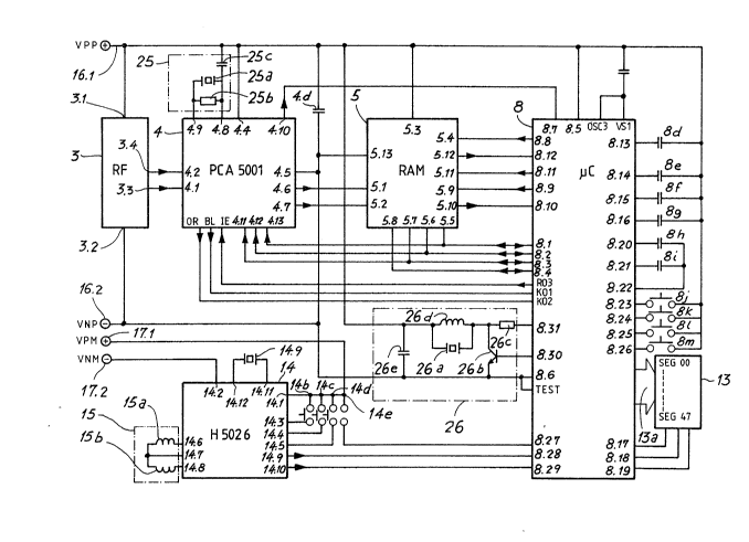
preferred embodiment of pager 1 according to the invention.
As already described hereinabove, pager 1 basically
comprises an antenna (not shown on figure 3), receiver
3, decoder 4, intelligent memory 5 and microcomputer 8.
The circuit 14 for control inputs intended for controll-
ing a timepiece 15 associated with the pager is also shown
on figure 3.
Receiver 3 is connected by terminal 3.1 to a positive
supply line 16.1 of the portable power supply 16 (not shown
on figure 3), its negative terminal 3.2 being connected
to a negative supply line 16.2 of the power supply 16.
In a known manner, radio broadcast coded message signals
are captured and demodulated by receiver 3 and the antenna
to which the latter is connected so that groups of binary
data such as those shown on figure 2A are generated at
the output 3.3 of receiver 3 and transmitted to the input
4.1 of decoder 4. Receiver 3 includes in its internal
circuitry an assembly (not shown on the figures but known
per se) for checking the tension of the energy source 16,
such assembly providing a signal indicating exhaustion
of such source on output 3.4 of receiver 3. The output
3.4 transmits in such case the exhaustion indication signal
,,
- 11 209~96~
to other circuits of pager 1 in order that a display read-
able by the user may be assured on the display 13.
Decoder 4 is connected to the positive supply line
16.1 by its terminal 4.4 and to the negative supply line
16.2 by its terminal 4.5. A voltage stabilization capacitor
4d is connected between terminals 4.4 and 4.5. The decoder
may be of the type PCA 5001 manufactured by Philips and
its task is to separate the selective call signal
information from the message information as such in the
coded message signals and to compare the call signal
information with the predetermined address information
stored in the decoder and individual to the pager under
consideration.
If the collective call signal information corresponds
to one of the stored addresses, every message code word
following the address code considered up to the following
address code word is transmitted in the form of serial
data from the output 4.6 to the input 5.1 of the intelligent
memory 5.
The output 4.7 from the decoder 4 furnishes a data
transfer signal in order to permit reading by the
intelligent memory 5 of data available at the output 4.6,
such signal assuming a high level or a low level at the
input 5.2 of memory 5. The message information furnished
to output 4.6 is introduced into the storage area 7 of
the intelligent memory 5 when a complete data byte has
been transferred from receiver 3 to decoder 4.
A resonator circuit 25 is connected to the decoder
4 through inputs 4.8 and 4.9 of this latter. It comprises
basically a quartz resonator 25a connected in parallel
to a damping resistor 25b and to the inputs 4.8 and 4.9.
The positive supply line 16.1 i.s connected to one of the
quartz resonator terminals 25a through a resonance capacitor
,
,
- 12 _ 2 09~g~l
25c. The resonator circuit 25 cooperates with the internal
circuitry of decoder 4 in order to form an oscillator
circuit which furnishes a periodic wave form of 32 kHz
for example to decoder 4 in order to determine the rate
of transmission of message signals from receiver 3 towards
decoder 4. As is well understood, other clock frequencies
may be used as a function of the transmission rate of
message signals. The resonator circuit 25 is also used
to furnish a clock signal to the microcomputer 8 and to
the intelligent memory 5. Such clock signal is furnished
to the microcomputer 8 via the output 4.10 of decoder 4.
The values of the resistor 25b and of the capacitor 25c
may respectively be 4.7 MQ and 10 pF.
Decoder 4 comprises a reprogrammable electrically
erasable memory of the EEPROM type (not shownl in which
are stored the system parameters of the decoder 4. Control
signals can be sent from the microcomputer 8 towards the
inputs 4.11, 4.12 and 4.13 in order to control the functions
of the decoder 4. One of the functions of the decoder
4 which may be controlled is the rate of bit transmission
between decoder 4 and the intelligent memory 5, such rate
going as high as 5000 bits/second. In such case, the message
information is stored in the circular buffer located in
the intelligent memory 5 without undergoing any other
processing ~such as comparison between the last two messages
which have just been stored).
The input 5.3 of intelligent memory 5 is connected
to the positive power supply line 16.1 while the input
5.13 is coupled to the negative line 16.2. The time base
for the intelligent memory 5 is determined by the clock
signal furnished by output 8.8 of the microcomputer 8 to
the input 5.4.
The intelligent memory 5 shows four terminals 5.5,
5.6, 5.7 and 5.8 respectively connected to corresponding
,
- 18 - 2~959~
terminals 8.1, 8.2, 8.3 and 8.4 of the microcomputer 8,
which assures a simple parallel connection with this latter
enab]ing the sending of control signals from the micro-
computer 8 to the intelligent memory 5 and the sending
back of message information stored in memory area 7 of
intelligent memory 5 towards the microcomputer 8 in order
that such message information can be displayed. Depending
on the nature of the control signal which is transmitted
terminals 5.5 to 5.8 may also control the intelligent memory
5 in order to furnish the microcomputer 8 with status infor-
mation in respect of the reception of message infarmation
by memory 5. Other control signals may control the latter
in order that it manipulates message information which
is stored therein as will subsequently appear herein.
A data transfer input 5.11 for memory 5 is also provided
in order to assure the simultaneous transfer of data towards
terminals 5.5 to 5.8.
An lnput 5.9 determines whether inputs 5.5 to 5.8
carry data or introduce control signals into the intelligent
memory 5. When a high level signal is present on input
5.9, the signals on inputs 5.5 to 5.8 are interpreted as
being control signals coming from the microcomputer 8,
while if a low level signal is present, the signals are
interpreted as constituting data.
A terminal 5.10 of intelligent memory 5 enables inform-
ing the microcomputer 8 that the memory is ready to receive
control signals. A high level logic signal on terminal
5.10 is interpreted by the microcomputer 8 as indicating
that memory 5 is ready for a further communication with
the microcomputer 8 while a low level logic signal is inter-
preted as signifying that memory 5 is still in the process
either of accomplishing a manipulation on the data or
another operation, or is transferring data to the micro-
computer 8.
~ :
,
_ 14 _ 2 09 ~ 6l
An output terminal 5.12 from memory 5 serves to provide
an interrupt signal to the microcomputer 8 in order to
indicate thereto its functional status in response to the
received message information or to the control signals.
A high level logic signal is sent to the microcomputer
8 if, for example, fresh or repeated message information
is received or if an unknown, forbidden or unperformable
function is required by the microcomputer. Such interrupt
signal may thus be used in order to indicate to
microcomputer 8 that a new operation is required, such
as for instance to announce the arrival of fresh message
information or the sending of a new instruction to the
intelligent memory 5. A low level signal indicates that
no new action is required by the microcomputer 8.
Such microcomputer 8 may be of a known type suitably
programmed. It is connected to the positive supply line
16.1 by its input 8.5 and to the negative supply line
by its input 8.6. An input 8.7 receives the clock pulse
train from the output 4.10 of decoder 4. An output terminal
8.8 furnishes a clock signal to the input 5.4 of the intel-
ligent memory 5.
Microcomputer 8 also comprises output terminals 8.9
and 8.11 in order to furnish control signals and to trans-
fer data as described hereinabove respectively to inputs
5.9 and 5.11 of the intelligent memory 5, while input
terminals 8.10 and 8.12 are provided in order to
receive respectively the acceptance and interrupt signals
of the intelligent memory 5 as described hereinabove.
A liquid crystal display 13 is connected to micro-
computer 8. It comprises segments numbered from 00 to
47 which are connected to the display driver circuit (not
shown on figure 3) of microcomputer 8 by a bus 13a such
that each segment may individually be controlled and that
the desired message information may be displayed by display
. - ,
209~961
- 15 -
13. Specialists in the art will understand that various
voltage values are necessary for the driver circuit in
order to control the various segments of the display 13.
Input terminals 8.13 to 8.16 are connected to the positive
supply line 16.1 through capacitors 8d to 8g in order to
provide these various voltages. Capacitors 8d to 8g may
have respective values of 220, 100, 100 and 100 nF.
Microcomputer 8 also comprises output terminals 8.17, 8.18
and 8.19 in order to furnish, in a known manner, control
and time base signals to the display 13 coming from the
driver circuit.
The input terminals 8.20, 8.21 and 8.22 are provided
in order to stabilize and smoothe the internal voltage
levels of the microcomputer 8. One of the terminals of
a capacitor 8h is connected to the input 8.20 while one
of the terminals of another capacitor 8i is connected to
the input 8.21. The other terminals of capacitors 8h and
8i are connected together to terminal 8.22.
The microcomputer 8 is also provided with user control
inputs 8.23 to 8.26, each one of which is connected to
the positive supply line 16.1 through switches 8j, 8k,
81 and 8m which may be actuated by the user. When this
occurs, a high level logic signal is applied to the control
inputs by the user, for instance when he wishes to put
the pager 1 into or out of operation, render it silent,
protect the message displayed by display 13 or delete a
displayed message as will be explained hereinafter.
It will be understood that various other user control
functions may be provided in this manner and that a separate
input is not necessary for each of such functions thus
provided; for example one or several switches or
push-buttons can be actuated according to a special sequence
in order to indicate to microcomputer 8 that a certain
function is to be performed.
209S9~l
- 16 -
The circuit 14 for control inputs and the timepiece
is connected to the positive supply line 17.1 from the
portable energy source 17 (not shown on figure 3) by
terminal 14.1 and to the negative supply line 17.2 from
supply 17 by terminal 14.2.
Circuit 14 also comprises inputs 14.3. 14.4 and 14.5
which serve to form supplementary user inputs in order
to enable the pager 1 to perform certain functions ordered
by the user and also to control the operation of the
timepiece 14 which is controlled by circuit 14. A special
sequence of signals applied to inputs 14.3, 14.4 and 14.5
or signals initially sent to other inputs may be used in
order to determine whether inputs 14.3, 14.4 and 14.5
control the operation of the pager or the timepiece 15.
Inputs 14.3, 14.4 and 14.5 are respectively connected to
one of the terminals of switches 14b, 14c and 14d, their
other terminals being connected together at input 14.1.
The switches may be provided under any form usable by the
user. Another switch 14e is connected between the positive
supply line 17.1 and an input 8.27 of the microcomputer
8 in order to indicate thereto whether it is the pager
or the timepiece which is being controlled.
Circuit 14 further includes two outputs 14.6 and 14.8
respectively connected to one of the terminals of the two
windings 1Sa and 1Sb of the timepiece 15. The other termin-
als of such windings are connected to a common return
connection 14.7. Those skilled in the art will understand
that in the example chosen herein windings 1Sa and 15b
belong to a bidirectional motor of an analog quartz time-
piece well known moreover, but that any other type of time-
piece may be provided, including a digital timepiece in
which case, as is well understood, a watch motor is not
necessary. Various other inputs may be provided for circuit
14 in order to control any other function of the timepiece.
: . :
~.
- 17 - 2~
Two other outputs 14.9 and 14.10 of circuit 14 are
respec:tively coupled to inputs 8.28 and 8.29 in order to
furnish the microcomputer 8 with data representing the
signa]s applied to inputs 14.3, 14.4 and 14.5. A quartz
resonator 14.9 is coupled to input 14.11 and to output
14.12 of circuit 14 in order to constitute a timebase for
the latter.
Pager 1 also comprises a warning device 26 coupled
to the microcomputer 8 in order that new message information
received by decoder 4 may be announced. An electrical
acoustic transducer 26a (buzzer) is connected by one of
its terminals to the collector of a switching transistor
26b and by its other terminal to the positive supply line
16.1. The collector of transistor 26b is also connected
to the output 8.31 of the microcomputer 8 through a polariz-
ation resistor 26c which may have a value of 18 kQ .
Normally, this output is maintained at a high logic level.
The emitter of transistor 26b is connected to the negative
supply line 16.2 and to terminal 8.6 of the microcomputer
8. The base of transistor 26b is connected to the output
8.30 of the latter. A choke 26d having an inductance of
45 mH, for instance, is connected in parallel with the
buzzer 26a. Finally, a voltage stabilizing capacitor 26e
having a value of 4.7 ~F, is connected between the positive
16.1 and negative 16.2 supply lines. In normal operation,
the output 8.30 is maintained at a low level and transistor
26b is non-conducting.
When pager 1 is to announce reception of a call or
the accomplishment of another function, a signal which
can have a variable wave form is transmitted by output
8.31 which generates a voltage at the terminals of the
buzzer 26a which thus will produce a first sound. A
different sound may be produced by the transducer 26 when
a signal is s-ent by the output 8.30 to the base of
transistor 26b which then begins to conduct. A different
~'.: ,-': " :
209~961
- 18 -
voltage is then generated at the terminals of the buzzer
26a and a second sound is produced. Such different sounds
can be used in order to announce performance of various
functions by pager 1.
Figure 4 shows a simplified schematic of the intellig-
ent memory 5 which basically comprises the unit 6 for data
processing, memory area 7, ROM 27, register stack 28,
the microprocessor interface 29 and the decoder interface
30. Terminals 5.5 to 5.12, already described, are
connected to the microprocessor interface 29 while terminals
5.1 and 5.2, also hereinbefore described, are connected
to the decoder interface 30. The input providing the clock
signal of 32 kHz to the intelligent memory 5 is connected
to the data processing unit 6. Furthermore, the micro-
processor interface 29 comprises a test input 5.13, a
capacitor 5d which may have a value of 15 nF being connect-
ed between the negative supply line 16.2 and an input
5.14 of memory area 7.
Intelligent memory 5 also comprises address and data
buses Se to Sk connected between the various internal elem-
ents of memory 5 in order to assure communication and data
transfer among themselves. ROM 27 contains the programs
necessary in order to bring about operation of memory 5.
In the embodiment described herein, memory area 7 is a
RAM having a capacity of 512 octets and intended to memorize
the message signals coming from decoder 4 and the internal
variables of the system, the stack of registers 28 forming
on the one hand a memory for temporary storage of data
used for manipulating message information in the memory
area 7 and on the other hand the stack pointer and program
counter.
It will be understood by those skilled in the art
that calls are normally transmitted more than once from
a central station to a given pager in order to guarantee
~' '
20~5961
1 9 --
good reception by such pager. Consequently, before writing
message information from decoder 4 into the memory area
7, intelligent memory 5 may advantageously compare such
received message information with two preceding messages
which the pager has just received. If the new message
information corresponds to one or the other of the two
most recent messages, the new message is not written into
memory area 7.
As already indicated and as shown on figure 5, it
is envisaged, in the embodiment of the invention under
consideration, to give the memory area 7 a capacity of
512 octets. Such a capacity is sufficient for conferring
to pager 1 sufficient information manipulation possibilities
so as to render it user friendly.
A capacity of 512 octets requires nine bits in order
to permit addressing of octets 0 to 511 in memory area
7. This signifies that for each write-in or read-out oper-
ation in this memory area, two transfers each of eight
bits are necessary since buses 5e to Sk have a transfer
capacity limited to 8 bits at a time. The program stored
in ROM 27 is adapted to work with such a double eight bit
transfer of which in the present embodiment only nine bits
are used. In fact, one may thus, without substantially
changing the program contained in ROM 27, easily increase
the capacity of memory area 7 up to a maximum of 65 kilo-
octets, which is a value largely exceeding the capacity
o~ 4 kilo-octets, which would already constitute a value
giving a large degree of user comfort. Such an extension
of the memory capacity would give the pager the possibility
of carrying out more control functions by the user and
also a greater capacity of storing received message infor-
mation.
Memory area 7 comprises address segments 7a, 7b and
7c (figure 5), segments 7a and 7b of which comprise
`' . . ~' ` : '
addresses 0 to 489 and are available for the storage of
message information received from decoder 4 and segment
7c comprises addresses 490 to 511 and contains internal
variables of intelligent memory S.
Address segment 7a comprises addresses 0 to 300 and
is used by the data processing unit 6 as a circular buffer
in order to store message information coming from decoder
4 so that the memory location assigned to the circular
buffer is initially sequentially filled with received
message information. Following storage of the message
information in each available address of the circular
buffer, the oldest message information is transferred at
the moment when the most recent message information is
received by intelligent memory 5. By default address
segment 7b occupying addresses 301 to 489 is used as a
protection section in which is stored message information
coming from the circular buffer which the user does not
wish to have transferred.
Address segment c comprises the following addresses
which are used by the data processing unit 6 in order to
manipulate data found in the memory area 7:
Address Function
510 This memory location contains the
address of the end of the last protected
message in the protection segment 7b.
508 Starting address of the circular buffer
7a, or Top-Qf-RAM ~TO~).
By altering the value stored at this
memory location, it is possible to
change the capacity of the circular
buffer 7a.
503 This register contains a data value
,. .
~' : ; ,
209S9~
which sets the number of octets per
second at which data is transferred
from the decoder 4 to the intelligent
memory 5 without treatment or interpret-
ation.
S00 Contains the address of the last octet
read when the data processing unit
6 was performing the instruction "PFIN
read decrement", as will be subsequently
described.
499 The data stored at this address is
used to determine which newly received
message information will be compared
with the previous two. This address
is initialised with the data 01 Hex
and may be transferred with the value
03 Hex when it is desired to make such
a comparison with the two newest mess-
ages.
In addition the following codes which may be stored
in the memory area 7 are interpreted by the data processing
unit 6 to have special meanings:
Code Meaninq
08 Hex Start and end of the protection zone
7b.
04 Hex, 84 Hex Header for a newly received message.
05 Hex, 85 Hex Header for a message to be erased from
the circular buffer 7a.
06 Hex, 86 Hex Header for a message that has been
. . ~
:
- , : . : : : .. -;. ::
'
~: .
- 209~961
- ~2 -
treated by the user of the paging device
1.
02 Hex, 82 Hex Header for a protected message that
has been transferred from the circular
buffer 7a to the protected zone 7b.
Reference will now be had to the operation of the
data processing unit 6, and the functions that are
successively performed by the intelligent memory 5 when
various instruction signals are received from the
microcomputer 8. As described previously, the microcomputer
8 is able to indicate to the intelligent memory 5 that
it wishes to send an instruction signal, by placing a high
level logic signal at the output 8.9. When the output
5.10 is at a high logic level, an instruction signal placed
at the outputs 8.1 to 8.4 is read by the intelligent memory
5 when a low-to-high logic transition occurs at the output
8.11. ~nder these conditions, the following functions
may be performed by the intelligent memory 5, where each
function code represents the logic state of the outputs
8.4 to 8.1 respectively:
Code Function
0000 The hardware of the memory storage area 7 is
reset. This function is sent to the intelligent
memory 5 on turn on of the pager device 1. The
size of the circular buffer is set at 300 bytes
by default. The reset state of the chip must
be maintained over at least two clock periods.
0100 The entire contents of RAM 7 are copied with
"." or another uniform character without adjusting
the circular buffer 7a. RAM is initialised as
above, but without resetting of the size of the
circular buffer 7a. This may be advantageous
if a buffer size other than 300 octets is chosen
'
2~9~961
- 23 -
by replacing TOR.
1000 The intelligent memory 5 uses outputs 5.5. to
5.8 as status flags to inform the microcomputer
8 as to the message information received from
the decoder 4. The outputs 5.5. to 5.8 have
the following signification:
5.5 Repetition of message 1
5.6 Repetition of message 2
5.7 New message
5.8 Error
0001 Writing stack pointer (PTA).- The RAM address
containing the PTA is copied with new data sent
to RAM 7 in 3 packets each of 4 bits. A change
in the actual value of the PTA will only occur
if all the packets of 4 bits are entered
correctly.
1001 Reading stack pointer (PTA~.- The stored value
of the PTA is read by the data processing unit
6, in 3 consecutive packets each of 4 bits.
The following functions serve to read from and write
to the memory area 7. The actual address of the memory
area 7 at which the message information is to be stored
or read from must firstly be put into the PTA register.
With a high logic level at the output 8.9 of the
microcomputer 8, the data present at the inputs 5.5 to
5.8 are treated as instruction signals. The message infor-
mation can subsequently be transferred to or from the
intelligent memory 5 when the logic level at the output
8.9 again goes low.
When an entire octet (2 packets each of 4 bits) has
been completely transferred, the position of the pointer
PTA stays unchanged. It is therefore possible to copy
. , -;, - .:
.
~ ;
2~959~1
- 24 -
an already read octet in the RAM 7 without the need to
change the position of the PTA. It is only upon the
transfer of the flrst packet of 4 bits, which are the four
most significant data bits with the leading edge of the
low-to-high logic level transition of the output 8.11 that
the PTA will be incremented or decremented and the address
changed of the RAM 7 to which it points.
Code Function
1010 RAM increment after reading - the contents of
the address to which the PTA is pointing are
read and then the PTA is automatically
incremented.
1011 RAM decrement after reading - the contents of
the address to which the PTA is pointing are
read and then the PTA is automatically
decremented.
0010 RAM increment after writing - data is transferred
to the intelligent memory 5 and then written
into the address to which PTA is pointing with
an automatic increment.
0011 RAM decrement after writing - data is transferred
to the intelligent memory 5 and then written
into the address to which the PTA is pointing
with an automatic decrement.
1100 PFIN decrement after reading - PFIN is a stack
pointer which indicates the end of the circular
buffer in the RAM 7. The instruction 1100 causes
the contents of the memory having the address
of PFIN to be read. After each octet is read,
PFIN is automatically decremented, so that each
octet is read once only. If PFIN has reached
:
-
209S961
= - 25 -
the last octet of message information, as
indicated by a header 04 H or 84 H, the logic
level of the output 5.12 goes high with an error
indicated in the status word upon the reading
of the least significant packet of 4 bits. It
is therefore possible to read all the message
information stored in the memory segment 7a up
to the end of the circular buffer.
PFIN is initialised at the value of TOR.
The following functions concern a single complete
message, rather than separate octets of message information
comprising the message. In order to separate the messages
from one another, the code 04 H or 84 H is written with
the data packet at the end of each message, and at the
start of the following message (header). The PTA must
contain the address of the header of the message to be
manipulated by the data processing unit 6, so that the
following instructions can be executed. If the PTA does
not contain this address, an interrupt signal will be
provided by a logic high level at the output 5.12 with
an error included in the status word.
Code Function
0101 Change header - a message is marked as a treated
message by changing the octet at the start of
the message to 06 H or 86 H. This can
advantageously avoid conflict between old message
information and newly received message
information.
0110 Message protection - a message can be protected
against a writing fault by copying it into the
protected area of address segment 7b. The message
header in the circular buffer is firstly changed
to 05 H or 85 H and then copled octet by octet
into the protected area. After this the message
,, :
~ - 26 -
is deleted from the circular buffer 7a automatic-
ally (no new code is needed).
0111 Message deletion - a message can be deleted from
the circular buffer or the protected zone. A
message is firstly marked for deletion by changing
the header to OS H or 85 H. It is then checked
whether this message is needed to be compared
with new messages received by the pager 1 for
preventing the storage of a repeated message.
When the message can be deleted all octets of
that message will be erased. If deletion is
not possible immediately, the message stays marked
and when possible is erased (this however requires
a further deletion command).
As can be seen from the foregoing, the intelligent
memory 5 according to the invention is thus adapted to
receive message information from the decoder 4 in real
time, so as to compare the received message with the
previously received messages and store chosen message
information in a memory area. The intelligent memory 5
is also adapted to copy, delete, move and otherwise
manipulate the stored message information and to communicate
and exchange data with the microcomputer 8 in a manner
which frees the microcomputer 8 from some of the constraints
connected with message information reception, storage and
manipulation.
t
: