Note: Descriptions are shown in the official language in which they were submitted.
2~9'~J97g
GRAY LEVEL ADDRESSING FOR LCDS
BACKGROUND OF THE INVENTION
Field Of The Invention
This inventi~n relates to addre5sing liquid
crystal displays (LCDs~ to provide a plurality o~ gray
shades or level~ for the displayed image and more
particularly to an apparatus and a method for providing a
very high number of gray levels ~or a fast-responding
passive matrix LCD.
LCDs are bacoming increasi~qly useful for
displayinq images not only in projection systems but as
screens for television receivers and computers. As a
consequence, there is a demand for even fas~er resp~nding,
high inormation content LCDs that can provide a very
large number of gray levels between white and black or a
large color palette.
~iscussion Of The Prior Art ;
One method of providing gray scale for an LCD is
known as rame modulation, exemplified by U.S. Patent Nos~
4,752,744 and 5,062,001 and an article by Y. Suzuki, et
al., "A Liquid-Crystal Image Display,"~1983 QI~L~1
~- 2s Technical P~ers XIv 32-33 (1983). I~ these frame
modulated systems the pixels forming the image on thQ
screen are turned "oni' and "off" in dif~erent frames
correlated to the gray level or shade of color desired.
When applied to faster-responding LCDs, however, frame
modulation causes "~licker" and "swim." Tha former i5
perceived by the viewer as if the image were being rapidly
- turned on and of~, and in the latter, the image appear~ to
have ripples or waves passing through it.
The so-call~d "pul~e-width modulation" gray
scale system, exemplified by U.S. Patent No. 4,427,978
.,
PDXl-21583.1 20030 0003 ~ ~
. .
:: .
~'
. . .
', : ` , ,: ~ :.
~9a978
issued January 24, 1984 and an article by H. Kawakami, et
al., 'iBrightness Uniformity in Liquid Crystal Displays,"
1980 SID Dinest o~_Technical PaPers XXI, 28 29 (1980), is :-
limited in the number oP distinct gray levels that it can
produce. PU1SQ_Widt~1 modulation is phy5ically incapable
of providing a number of gray levels on the order o~ 256
which is desira~le to bring out the ~ine detail of image~
required in "multimedia" applications o~ LCDs. In puls~
width modulated systems, the pulse5 become narrower and
the high frequency content of the drive signals increases
with the number of qray le~els. These hi~her frequsn~ie~
are cut of f by the low-pass RC ~ilter action of the LCD
panel, which makes it diPficult to realize more than about
4 to 7 gray levels on the display.
1~
SUMMARY OF THE INVENTION
It is therefore an object of this invention to
overcome the difficulties of prior art systems hy
providing a very large number of gray levels f~r ~aster-
~o responding, high information, rms~responding, passiv~
~` matrix LCDs.
More particularly, the method and apparatus ofthis invention provide a number of gray levels for an LCD
by modulating the amplitude or pulse height of the display
column drive signals.
As will be hereinafter described, the "pulse~
: heiqht" or amplitude modulation addressing systems of this
invention may be accomplished either in a "split interval"
mode or in a "full interval" mode. Each such mode may be
employed in either "standard" addressing methods or th~
"Swift" addressing method described in applicants'
copending application for U.S. Patent, Serial No. 678,736,
~iled April 1, 1991.
:
PDXl-21583. 1 20030 0003 `
,
;'`
` : " : . , , :
2~3 J978
~11 these methods and the apparatus
implementations thereof have in common the provision o~
means for qenerating and applying column signals who~a
amplitudes at a~y given tim~ are directly related to the
~Igray~ level or shade of color de5ired to be dîsplayed ~y
the pixels o~ the LCD panel and which are applied to thQ
electrodes by mult.ilevel drivers.
T~e advantage of pulse-height modulation in any
of ths forms described is that no matter how many gray
levels are generated, there is no siqnificant increasa in
high frequency components in the column signals.
BRIEF DESCRIPTION OF T~E DRAWINGS
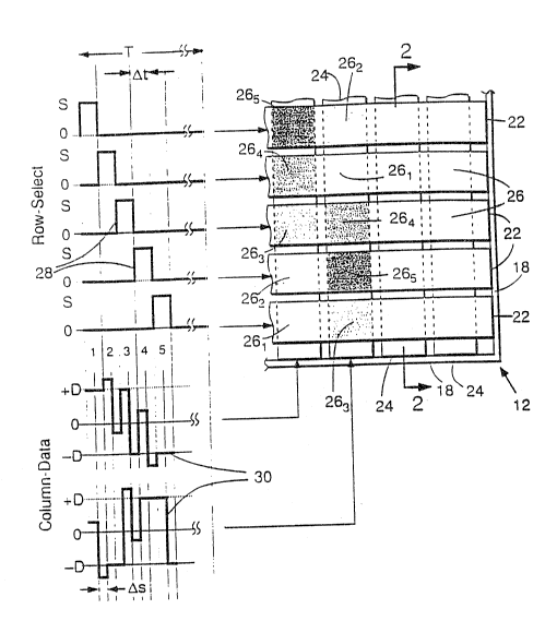
Fiq. 1 is a semi-diagrammatiC plan view of a
portion of an LCD panel with a schematic representation o~
idealized signal5 applied to some of the row and column
electrodes accordinq to the method o~ this invention.
Flg. 2 is a cross-sectional view as 5een from
line 2-2 of Fig. 1.
Figs. 3A and 3B are schematic representation~ o~
the idealized voltages across a pixel comparing the prior
art pulse-width modulation method (3A) with the puls~-
-~ height modulation method of this invention in the splitinterval, standard addressing mode (3B~, showing th~
different voltage levels resulting from the application of
signals to tha row and column electrodes of Fig. 1.
Fig. 4 is a qraph o~ the normalized column
voltages, plotted as a function of the gray level fraction
computed according to the pulse-height modulation method
of this invention in the split interval, standard
addressing mode.
Figs. 5A and 5~ are schematic representations o~
portions o~ idealized column signals respectively
comparing those of tho prior art pulse-width modulation
PDXl-21583.1 20030 0003
''; ~
- . '.: ' '~: ': ,, ~ . :
209a9rl~
m~thod (5A) with the method of this invention in tha split
interval, standard addressinq mode (5B) as applie~ to the
col~mn electrodes of Fig. 1.
Figs. GA and 6B are schematic representatlon~ of
portions of idealiz~d column signals respectivaly
comparing those o~ tha prior ar~ pulse-width modulatio~
method (6A) with the method of this invention in the split
intexval, "Swift" addressing mode (6B)~
Flg. 7 is a semi-dia~rammatic ~lan view si~lar
to Fig. 1 of a portion o~ an LCD panel with a schematic
repr~sentation of idealized row and column signals
generated and applied according to the method of thls
invention in the ~ull interval, s~andard addressing ~ode
and with a portion of a matrix of information elements
superimposed over the matrix of pixels.
Fig. 8 is a view 5imilar to Fig. 7 but with a
schematic representation of idealized signals generated
and applied according to the method o~ this invention ln
the full interval, "Swift" addressing mode.
~o Fig. 9 is a generalized ~lock diagram of
apparatus for generating and app}yinq signals to a passiv~
flat panel display, such as is shown in Fig. 1, in
accordance with this invention.
Fig. 10 is a block diagram of the controller o~
the apparatus of Fig. 9.
: Fig. 11 is a block diagram of the column driver
interface of the apparatus of Fig. 9.
Fig. 12 is a block diagram of the column signal
generator of the apparatus o~ Flg. 9 ~or operating in the
split interval, standard addressing mode.
Fig. 13 is a block diagram of the column signal
generator of the apparatus of Fig. 9 for operating in the
split interval, Swift addressing mode.
pDx~-2ls~3~l 20030 aoo3
::~
.
;
:
2i~ ~39'~
Fig. 1~ is a block diagram o~ th~ column signal
generator o~ the apparatus of Fig. 9 for opara~ing in tho
full inter~al, standard addressing mode.
Fig. 15 is a block diaqram of the column signal
generator of tha apparatus of Fig. 9 for operating in the
eull inter~al, swift ~ddressing mode.
Flg. 16 is a more datailed block diagram and
schematic representation of the dot product ~en~rator,
adjustment term generator and combiner of the column
lo signal generator of Fig. 15.
F~g. 17 is a more detailed block diagram and
schematic representation of a correlation sta~e o~ th~ dot
product yen~rator of Fig. 16.
DESCRIPTION OF THE PREFERRED EMBODIMiENTS
LÇD Panel Characterlstics
The method of this invention is applied to a
typical flat panel display 12 (Fig. 1) of the type
utilized in overhead projector panels, laptop computer
screens and the like. High information content panels o~
this type operate through direct multiplexed, root-m~an
square - responding (rms-responding) electro-optical
ef fects , such as the twisted nematic (TN), ~upertwisted
nematic (STN~ or superhomeotropic ~SH~ liquid crystal
display (LCD~ ef~ects.
Such panels typically comprise a pair o~ :
opposed, parallel, spaced glass plates or substrates 14
and 16 (Fig. 2) between which is a cell gap 20 where an
0 electro-optical material 21 such as a liquid crystal is
disposed. A seal 18 around the edges of substratPs 14 and
16 serves to confine th~ liquid crystal material withln
the cell gap 20.
P~Xl-21583.1 20030 0003
~ :~
20~a978
Liquid crystal d~splay panels are charactQriz~d
by an inhPrent time constant, i.e., the tim~ re~uired ~or
the liquid crystal director to return to its e~uilibrium
state after having ~een displaced away from it by a
dielectric torque induced by an electrical field. The
time constant, r ~ is defined by = ~d2/K, wherP ~ is an
averaqe viscosity of t~e liquid crystal materia}, d 1~ the
cell gap spacing or pitch len9th and K is an average
elastic constant of tha liquid crystal material. For a
conventional liquid crystal material in a ~-10 ~m cell qap,
the time constant r is on the order of 200-400 ms
(milliseconds). Also in typical multiplexed LCD , the
information is refreshed at a rate of 60 Hz corresponding
to a frame period of 1~60 seconds or 16.7 ms~
Relatively recently, LCD panel time con~tants
have been reduced to below 50 ms by makin~ the gap, d,
between the substrates thinner and by using newly
; synthesized liquid crystal materials which have lower
viscosities and higher elastic constants. These faster-
responding panels, genPrally designated as any pan~l wit~
a response time below 150 ms, make pos~ible high
; in~ormation content displays at video rates.
n one common embodiment of LcD panel, a matri~
comprised of transparent electrodes is applied to the
inner surfaces of the substrates, typically arranged in a
plurality o~ horizontal or row electrodes 22 on the inner
: surface of substrate 14 and vertical or column electrc~es
~:: 24 on the opposed inner surface of substrate 16 (Figs. 1
and 2~. The areas where the row and column electrodes
overlap or cross create a matrix of picture elements or
pixels 26 by which information is displayed on the p~nel
12. The arrangement of overlapping electrodes may take
:~ many forms, such as concentric rings and radial llne~,
although a matrix of row and column electrodes as
, ~
PDXl-21583.1 20030 0003
., .
,- , . - . ~ `
' . -
2~93~7~
disclosed is the mo5t common pa~tern. High information
con~en~ displays require large number5 of pixels to
portray text and/or graphic imayes. Matrix LCDs having
480 rows and 640 columns forming 3Q7,200 pixels are not
uncommon and have provided high in~ormation content panels
of approximately lO~-inch ~27cm~ diagonal size.
Information is displayed on panel 12 by the
relative degree of transmittance of li~h~ through the
pixels, either from a light source on a side of panel 12
opposite from a viewer or by virtue of r~flected light.
The optical state o~ a pixel, i.e., whether it appears
dark, bright, or an intermediate shade is determined by
the orientation of the liquid crystal directors in the
pixel ~rea 26 ~Fig. 2). The direction of orientation of
the liquid crystal material 20 in the pixel area 26 and,
hence, the transmittance of the pixel is changed by th~
application of an electrio31 field across the pixel. In
direct multiplexed addressing techni~ues commonly used
with matrix LCDs, the pixel ~Isees~l an electrical field
proportional to the difference in the signals, or
volta~es, applied to the electrodes 22 and 24 on opposit~
sides of t~e pixel. Those signals o~ appropriate
frequency, phase and amplitude are determined by the
information to be displayed from a video signal or other
source.
"Sta~dard" Addressinq
In standard addressing of an LCD panel of N-
number of rows and M-number of columns without gray
levels, row select pulses o~ amplitude +S and width ~t are
sequentially applied to the row electrodes, which are
otherwise held at no signal or zero voltage during the : :
remainder of the frame period (Fig. ll. As used herein,
~ "select" means that a non-zero voltaqe is applied to the
.~
pDxl-2lsa3~l 20030 0003
:~
:
:
row. Width ~t is the ~chara~Q~i~t9i~time interval" ~or
standard addressing and is equal to the frame period, T,
divided by the number of row electrodes, N, thus T/N.
During the same frame period, the oolumn
ele~trodes are each driven with a signal which is
determined by the info~mation to be displayed. For an
"on" or select pixel determined to appear bright or ha~e
high transmittance, the column voltage is -D during t~e
time interval that the row containinq the pixel is
addressed with a select pulse. For an "off" or non-select
pixel determined to be in a dark or low or non-
transmittance state, the column voltage is ~Do Sinc~ the
voltage applied to the pixel ls the difference between the
row and column voltages, a select pixel will "see" a pulse
height or amplitude of S~D and a non-select pixel will
"see" a pulse height of S-D during one characteristic tim~
in~erval each frame period. During the remaining
characteristic time intervals of the frame period, the
pixels "see" voltage levels switching ~etween +D and D.
For maximum selection ratio, which is the ratio
of the select or "on": rms voltage applied across the pixel
divided by the non-select or "o~f" rms voltage applied to
- the pixel, the signal amplitude, S, of the row select
signal is optimally related to the amplitude D of thQ
column signal by:
9 = ~ D,
and D is related to the non-selec~ rms pixel voltag~ Vn,
by: :
D=~nll~ I
; 30 where N is the number of multiplexed row6 in the display.
The addressin~ tech-~Lque referred to h~rein a~
~: '/standard~' addressing is described in detail by P. Alt and
PDXl-25503.1 20030 0003
~ ` , .
: . ' .
:, . . . : . .
' ' . ' ~
~0 9 3978
P. Pleshko, "Scanning LimitationS of Liquid Crystal
Displays" in IEEE Transactions of Electron_Devices
Vol. ED-21, No. 2, February 1974, pages 146-155.
Subsequent improvements that have been made to eliminat~
D.C. voltages across the di5play and ~o decrease the power
supply voltages and maximum voltage limits of the driv~
circuitry do not alter the basic principle of operation or
its applicability to the gray level mathods of this
; invention.
rn the prior art pulse-width gray scale
addressing system (Fig. 3A), a column signal of amplituda
-D, correspondinq to an 'lon" pixel, is applied for only a
fraction, f, of the row select time interval, ~t, and a
column signal of amplitude +D, corresponding to an llof~l'
pixel, is applied for the remainir~ fraction, l-f. During
t~e row select time interval, ~t, the amplitude of the
: signal ~Iseen~l by the pixel is s+D for the fraction, f, and
S-D for the remaining portion, l-f, of the time interval
(Fig~ 3A). Since the pixel see~ a signal amplitude of
2~ either +D or -D over the remainin~ time intervals of th
frame, the rms voltage across the pixel averaged over one : :~
~rame period is intermediate between the rms voltage when .
:~ the pixel is "on" and the rms voltage when~ the pixel i
off." The result is a pixel response in an inte~mediate
optical state of transmittance or gray level. The
fraction, f, also des~ribe~ the relative position o~ the
intermediate pixel voltage between the rms "o~f 1I pixel
: voltage and the rms 'lonl~ pixel voltage; that is, f i~ th~
gray level fraction varying between zerc and 1 (Fig. 4~.
It will be noted in Fig. 3A that the pulses :~
become narrower and the high frequency content of the :~
column drive signals increase~ with the number of gray
levels. Because the higher fre~uencies are removed by the
~ inherent low-pass RC ~ilter action of th~ LCD panel, it i~ --
-,:',
PI~X~.-215~3.1 20030 000
~ ';
: . ,' .: , ~ :
, : ' .. ~:: , ' . .
~: , :
2 b9 39~
very difficult to r~alize mora than about four to seven
real gray levels on a display with the pUlse-width
modulation method.
"Swiftl'_Addressinq
The aforementioned U.S. Patent application
describes a Swift addressin~ system for LCD panels, whlch
doe not require the single, high amplltude row s~lact
pulse that is utilized in standard addressing and ca~s~s
o ~rame re~ponse. The row signals of swift addressing are
characterized by:
1. A common ~rame period, T, and signals that are
pre~erably orthonormal;
2. More than one row select pulse per frame period,
the pulses pre~erably uniformly distributed over
the frame period; and
3. Sl~nals phased in such a way that a plurality o~
rows are "sel~cted" (l.e., recaive non-zQro
voltage) at any one time.
The most general kind of functions satisfying
the above Swift criteria are continuous functions where :
the voltage levels are a continuous function of time. An
example of such functions would be tha orthonormal sin~
; and co~ine functions o f various frequencies. For the~o
types of functions there is no characteristic time
interval ~nd the sampling must be done on a continuou~
basis. These types o~ functions are well suited for
analog implementation of Swift addre~sing.
Another class o~ function~ whi~h are
particularly amenable for digital implementation o~ Swift
addressing are the orthonormal bilevel functions which
alternate over discrete time intervais, at, between two
constant non-æero voltage l~vel~, preferably of tha sa~e
magnitude but opposite sign. These functlons can be
PDXl-21~83. 1 20030 0003
'
~ .
''` . , , : '
- ,
~1~9~7~
represented by Hadamard matricas, which are s~,~uare
orthoqonal matrices with the elements -1 and -~1. Th~P
characteristic time in~erv~al, ~t, of such a function is the
frame period T divided by the order o~ the Hadamard
matrix. The order of any Hadamard matrix is divisible by
4, anA thus can be represented by 4t, where t is a
positive integer. Thus the characteristic time int~rv~al ~t
is given ~t=T/(4t~.
Walsh ~unctions are a subset of Hadamard
matrices haYing an order that is a pow~r o~ 2, i.e., there
are 2s time interv~als where s is an integer, such that 25
~<N<2s. The characteristic time interval in this casa is
~t=T~2s. Walsh ~unctions are particularly useful for Swi~t
addressing because fast Walsh transforms (FWT) are known
which can considerably simplify the number of computatlons
required to generate the column signals.
Another subset of the Hadamard matrices which
are particularly use~ul ~or Swift addressing are thosQ
that are constructed fro~ maximal length pseudo-rando~
binary sequences. Except f or one row and column, tha~e
: are circulant matrices in which a new row function can be
~enerated Prom a previous one simply by phase shifting it
by one time interval. Like Wal~h functions, this special
type o~ Hadamard matrix has an order that is a power of 2,
and thus the characteristic time interval is also given by
: ~t=T/2s. Almost circulant ~adamard matrices Gan also be
generated from Legendre ~equences which have matrix orders
that are given by (p~l)=4t, where p is a prime number. In
this case the characteristic time interval would be g~ven
by ~t-T/(p+l). Almost circulant Hadamard matrices can also
: be qenerated from twin-prime sequences which have matrix
orders of p(p+2)+1, whare p and p+2 are both prime
numbers. Here the characteristic time interv~al would b~
given by ~t=T/[p(p+2)+1~-
: .
PDX7.-21Sr33.1 20030 OOU3
.'
'
!. :
.
~ ?
2 ~ 7 ~ :
Another class of Swift functions are the
multilevel orthonormal functions where the row voltage can
~ttain three or more different volta~e levels during
discrete time intervals. Exampl~s of these types o~
functions are the Haar functions and the slant ~unctions
which are both well known in diqital signal processing for
image transmission. Other multilevel functions can be
derived by appropriately combinin~ other orthonormal
function sets. An example of thi5 would be the mixed
Walsh-Haar series. Multilavel pseudo-random sequences are
also known.
Three-level Swift function~ can be generated
erom the two-level Hadamard ~unctions by expanding the
si~e of the matrix and adding time intervals where the
voltage lev~l is zero instead of ~1 in such a way that the
matrix remains orthogonal and the row is selected at
uniform times over the frame period, referred to as tho
sparse matrix expansion. This can simpli~y th~ hardware
implementation of the method because the product of
information element and row voltage need not be taken over
those intervals where the row voltage is zero.
For example, a 4x4 Walsh matrix could be
transformed into an 8x8 Swift matrix by inserting a colu~n
of zeros after each Walsh column for the upper half and
repeating this configuration for the lower half by
cyclically shifting it by one column.
Larger matrices can be similarly generated by
adding more columns o~ zeros between the Hadamard columns
and appending an equal number o~ cyclically shifted
versions to the bottom of the matrix. For example, adding
two columns of zeros after each Walsh column of the 4x4
;~ matrix and appending two shi~ted matrice~ onto ths bottom
results in a 12x12 Swift matrix.
PDXl-2158~.1 20030 0003
, ' :
,'
: .,
.
2~9 ~9 78
It should be apparent that this operation
preserves the orthonormality condition as well as
uniformly distributes the selection intervals throughout
the frame period, as per Swift conditions 1, 2 and 3,
S above. The characteristic time interval for these types
of Swift fu~ction i5 tha frame period divided by the ordQr
of the matrix (e.~., t~ number of ~atrix rows),
Even more Swift row function5 can ba gen~rat~d
from the ab~ve ~entioned one~ by interchangin~ matrix
rows, neqatin~ matrix r~ws (i.e., multiply.ing them by ~
inter~hanging matrix columns, negati~g matrix columns, or
any possible combination of ~ll eOur of these operations.
For Swift row addressing signals der.ived from : :
other sequencPs, the characteristic time interval ~t is
def.ined as the frame period divided by the number of
elements in the sequence. The Swift column voltage at any
time interval, ~t, is proportional to the sum of the
products of the row voltage5 at that time interval and the
desired information states (+l for "off" or -1 for "on")
of the corresponding pixels at the intersection of that :: -
column and those rows. The Swift column voltages thu3 can
assume many values, not just the two, +D and -D, which
char~ct~rize standard addressing. ~:
Although prior art pulse-width modulation can b~
ZS applied to Swift addressing to achieve gray levels, it
suffers from the same problem, namely that the ~arrower
pulses are too severely attenuated by the low-pass RC
filter action of the LCD panel to ever reach the pix~l.
The end result is that an insuf ~icient number of gray
levels are available on the display to portray images to
the desirPd fidelity.
PULSE-HEIGHT MODULATION
pDxl-2lsa3~l 2~03a 0~03
,, '.
'
,~, . .:, , . :
: -. ~ :
~Q4~ 3978
In order to provide a substantially greater
number of disp}ayable gray levels without the concomitant
increase in high frequency content of the column driv~
signals, the present invention provides method o~ and
means for applying variable voltage levels to the display
columns which levels are constant over time intervals
subs~antially longer than the shortest time intervals that
would have been utilized in generating the same number of
gray levels by pulse-width modulation techniques. ~h2
~0 methods and means o~ this invention are used to determine
the values of the column voltage levels and their timin~
in order to ensure that each pixel of the display will
ad~pt its predetermined gray shade without interacting
with the gray levels of other pixels of the display.
The gray level mathods and apparatus of this
invention encompass two different modes to determine th~
values of column voltage levels and their timings in order
to render the desired gray levels ~or each pixel on th~
display. In the split interval mode, two column voltage
levels are computed for each characteristic time int~rval
~t. I~ the full interval mode, one column voltage level is
compu~ed for each charactaristic time interval and at
least one row is designated as a "virtual" or phantom row
across whose virtual pixels voltagas are determined by the
~ 25 information states or elements of all the other pixels in
: its column.
. ' .
: Split Interval Mode - Stand~rd Addressinq
In the split interval mode (Figs. 1, 3B, 5B) th~
characteristic time interval, ~t, i5 divided into two ~:~
subintervals, as and a different column signal or voltage
is applied over each subinterval. Preferably the two
subintervals are of equal length to maintain the 10WQSt
possible frequency content of the column signal.
POXl-21583 . ~ ~0030 0003
';:;
` :
- ~ `` - ; :, .
.
- : ~ ,' , : , .
- . . : -
': : , ' ~ : : -
2 ~ 7 ~
For the split interval mode, the amplitudes or
voltage levels of the column signals, X and Y, 3pplied
durinq the two subintervals are chosen to provide the same
rms voltage across the pixels durinq each time interval,
~t, ~hat would have been applied if ~ulse-width modulation
had been used. The resulting rms voltaye across the
pixels averaged over the entire frame period, T, ~ill also
be the same as if pulse-width modulation had been used
and, hence, the gray levels will be the same.
The X and Y column voltages according to the
method of this invention will satisfy the two conditlons
that the rms pixel volta~es durin~ both the selected and
non-selected intervals match the rms pixel voltages during
the corresponding intervals according to the pulse-width
modulated method if they are determined by the equations:
:,
X=D(1-2~+2~f~1-f)),
Y=D(1-~-2 ~ )-
Flgs. SA and 5B compare a portion of a pulse-
20 width modulated column signal with the pulse height
modulated column signal o~ this invention. The values o~
the X and Y column voltages are obtained from ths graph o~
Fig. 4 which plots the normalized column voltages, X/D and
Y/D, as a function of the gray level fraction f. E:very
25 gray level fraction, f, i~ a~socia~ed with two voltage
levels, X and Y, except for the special cases where ~-0
~"off") and f=l ("on"; in which X=Y (Fig. 4). Voltag~ X
is arbitrarily applied over the first tima subinterval,
~s~, and voltage Y is applied over the second time
30 subinterval, QS".
In operation accord.ing to the method of this
invention in the standard, split intenral mode, th~ rows
PDXl-21503.1 20030 0003
a ~ ri 8
of display 12 (Flg. 1) defined by row ~lectroda~ 22 axe
selected sequentially by thP application of the pulses of
amplitude S of row signals 28. t;uring the first time
interval, at, that the uppex~nost row in Fig. 1 i5 being
selected, column signals 30 of amplitudes X and Y (both
equal to D, for example), related to the desired gray
level of the ~ppermost lePt pixel of dlsplay 12 are
respectively applied to the left mos~ column during the
first two subintervals, ~s. The result is that the voltage
that the upper, left pixel 26 sees has a pulse height o~
S-D during the first time intPrval, and, therefore is
"off" or dark, as denoted by reference numeral 265.
Coincidentally, as a row select si~nal is
applied to each successive row in the display during
sucoessive time intervals, the appropriate column signals
X and Y related to the desired gray levels of the
respective pixels will be applied during successive
su~intervals, ~s, to the respective columns. In the
example of Fig. 1, the desired grav levels vary from 1 Por
"on" or bright to 5 for "off" or dark, with 2, 3 and 4
rapresenting intermediate gray levels. The correspondinq
values o~ "f" ~Fig. 4~ are respectively 1, 0.75, 0.5, 0.25
and 0. The shading and the subscripts for pixels 26 in
the two lePt columns of Fig. 1 are representative of the
desired gray levels resulting from the generation and
application o~ row and column signals of proper magnituda
and timing according to the above described method.
Fig. 3B shows a portion o~ the idealized pix~l
voltage wave~orm, transformed according to the gray level
method of this invention from a corresponding portion o~
the pixel voltage wave~orm o~ the pulse-width modulated
gray level method of the prior art, as shown in Fig. 3A,
In the example given above, the number of time
subintervals in the frame period and hence the f~equen~y
PDXl-2151i3.1 20030 0003
'
' : . , ' , ' . ~ . :' ' " ` ' ` .
: . ": ' ' , ' ` -
::
2Q7~ ~37~
content of the column signa~s is twic~ that of the
standard LCD drive without gray levels. Even though most
of these frequencies are low enough to be passed by the RC
filter action of the LCD, under some circumstances it may
be advantageous to halve such frequency by doubling th~
width of the time subintèrvals and using two ~rame periods
to supply the required voltage levels to the di5play. For
example, the X and Y levels could be supplied alternataly
to the columns, as indicated above or alternatively, all
of the X voltage levels and all of the Y voltaqe l~vel~
cuuld be alternatiYely applied to all the time interYals
of successiva rame periods. In such cases the frequency
content of the column signals would be the same as in
standard LCD drive methods without gray levels.
Split Interval Mode - Swift Addressinq
As mentioned above~ one method to achieve gray
levels with Swi~t addressing is to employ a pulse-width
modulation technique. U~ing this technique the
characteristic time interval, ~t, is broken up into un~qual
subintervals, ~s, whose lengths successively increase by
powers o~ two ~nd where the voltage level in each
subinterval is determined by the information states of the
respective bits in the gray level "words" for a:Ll pixels
in the display column.
For example, Fi~. 6A illustrates the column
voltage level~ in one characteristic time interval for a
4-bit gray scale, corresponding to 16 gray levels. tThare
are o~ course many such time intervals in the frame period
3~ of tha column signal, and aach one will generally have a
di~ferent set of voltage levels.) In the time interval
illustrated in Fig. 6A, the four voltage levels are
symbolically represented by A, B, C, and D, where A
corresponds to the least significant bit (~S~) o~ the gray
~; Pl~Xl-21Sa3.1 20010 OOU3
~ - .
,~
:: ' ~ , .. : : , :., :: ., ., : :
2 ~ 91~9 7 8
scale and D corresponds to the mQst significant bit (MS~).
The narrowest time subinterval corre5ponding to the LSB,
~SL~ has many high frequency components which reduce it~
effectiveness as determining a gray level because o~ the
S inherent RC ~`ilterin~ action oP the LCD panel.
The gray level method ~f this invention avoids
such hiqh frequency components by employing a column
signal as illustrated in Fig. 6B, which signal has only
two voltage levels, X and Y distributed over much longer
lG time subintervals, ~s.
Similar to the procedure used for standard
addressin~, the values o~ ~ and Y are hasad on the column
signal that would have been produced had the pulse-width
modulation system been used.
In one implementation of Swift addressing, the
display rows are driven with bilevel Swift signals during
characteristic time intervals, ~t, where the row voltag~
levels are either ~D or -D but are never zero (Sse Fig. 8
~or example). The resulting pixel voltage is the
difference between the column and row voltages, so in
dete~mining the rms pixel voltage over the characteristic
time interval two cases must be considered: one when the
row level is -D and the other when the row level is +D.
In order that the rms pixel voltage of the gray
2S level method of this invention illustrated in Fig. 6B, be
the same over the characteristic time interval, ~t, as the
pulse width modulated mathod of Fig. 6A, the column ::
voltages, X and Y of the former are calculated by:
X=2 [P+~] '
and
Y-2 ~P-~]
where p and q are related to A, ~, C, and D by:
PDXl -21Sa3 .1 20D30 0003
.
:
:. : . '. :` :' :
:` . ~ . . ' . . ' :~
: ' - ' ': ,' ' - ' ' ' ' : '-' -' ' : ' ' ': ' ' ' ' : ' :` ' -: -
:':: .
~: ~ ' : :
'` , ',: ~
2a t~ ~ 7 ~
19
~=125l A~2B~4C~8DlI
2 {~2~2B2~C2~8D2)-
For the example illustrated in Figs. 6A and 6~,
A = ~ 88, B = 0.944, C = 2.~60 and D = -1.416. Fro~ th~
S above equations, p = 0.252 and q = 5.822 and, finally/ X
= 1.576 and Y = -1.828. The above e~uations can easily be
extended to include more gray levels. For example, for 8
bits of gray scale, i.e., 256 gray levels, E, F, G and H ~
terms would be added to the above equations with ~ :
respective multipliers of 16, 32, 64 and 128, and the
fraction 2/15 chanqed to ~/255.
A more ~eneral statement of the above equations
for determining p and q which would accommodate varying
numbers of qray levels is:
p_ '2 ~2~-lG~,
and
2 1~
where n is the numher o~ gray bits in the gray level word,
g is the position of t~e gray bit in the gray level word,
and G~ is the column voltage level for the geh gray ~it.
In the case of 16 gray levels.illustrated in
Figs. 6A and 6B, the narroweat pulse width in the colu~n
signal of this invention (Flg. 6B) is 7.5 times wid~r than '.
the narrowest pulse in the pulse-width modulation m~thod
of Fig. 6A, resulting in 7.5 t~mes lower fr~quency
components in the column signal an~ much less filtering by
the LCD panel. This ~actor for the general case of n bits
of ~ray scale is equal to (2" 1)/2 and would be 127.5 for
the example of 8 gray bits or 256 gray levels. ~;
;~ PDX~-215~. 1 20030 0003
~' : ' ~," : ' -
:` : : : ' .: :: . ' ::- ~ ' . ''
: ' ' ' , ' : '`'`' ... , : '
; .~ .
2 0 ~3 ;~ ~ 78
As in the standard addressin~, split interval
mode, row signals which are independent o~ the information
to be displayed are applied to the row electrodes
coincidentally with the application of column signals
S represen~ative of such information to the column
electrodPs, resulting in the pixels displayinq the de~ired
information in the appropriate gray levels.
Full Enterval Mode_- St~ndard Addressin~
one of the charact~ristics of the Swift
addressing method described in applicants' pending
application, U.S. Serial No. 678,7~6, is a provision o~ an
information matrix (generally desiqnated 31 in Figs. 7 and
~). Matrix 31 is made up o~ pixel information elements 41
~5 which correspond one-to-one to the matrix of pixels 36
shown in Figs. 7 and 8 at the intersections of rows 32 and
columns 34. The pixel information element 41
correspanding to the pixel 36 at each of said
intersections designates the desired "state" or gray level
of the associated pixel.
In the full interval moda o~ the gray level
addressing system of this invention, the values, I, of
pixel information elements 41 may vary between ~1 for "on"
(or, for example, bright transmittance) to ~1 for "off'~
(or, for example, dark transmittance). Any value betweQn
these lower and upper limits desig~ates a gray level which
it is desired that the associated pixel display.
In addition to the pixel information elements
associated with the "real" rows 32 and columns 34 de~ining
"real" pixels 36, the information matrix 31 of thi
invention for operating in the full interval mode requires
at least one "virtual" or phantom row 39 ~Figs. 7 and 8)
which crosses or overlaps extensions o~ columns 34 to
provide virtual pixels 37.
PDXl-21583.1 20030 0003
:.
', ' :' `' ` ' ~ ' ::
: :
., , '' ~ '
'
2 ~ 9 7 8
Wlth every virtual pixel 37 there is associated
a virtual information element 42 whose value, V, i5
determined hy the values, I, of pixel in~ormation elements ~
41 of all the ot~er pixels in that column. For the ca3e ~ :
of one virtual row, the value of the virtual information :~:
element, V, associated with each column, is determin~d
~rom:
V=~
i l .
where N is the number of rows in the display, and Il is the
lo value of the plxel in~ormation element o~ the i-th real
row.
From the above equation it can be seen that the
virtual information element i3 zero when there are no
pixels with gray levels in the column (i.e., all pixels
are "on" or ~off").
The column signals depend upon the information
to be displayed. In the full interval mode with standard
addressing the column signal at any time is proportional
to the value of the information element of the selected
row, real or virtual (I or V). More precisely, the column
signal, G, for each column at the time interval, ~t, when a
real row is selected i5 given by:
G=DI ,
and during each time interval that a virtual row is
selected, ths amplitude of said column signal G is
dete~nined by:
G=DV .
When the gray level method of this invention
operating in the full int~rval mode is applied to displays
using standard row addressing signals (Fig. 7) the
characteristic time interval, ~t, is t~e frame period, ~,
divided by the sum of the number o~ real display rows, N,
PDXl-21.$~3, 1 201:\3D 0003
.
. . ~
- , ' . -' ' .. . :. . ': ,,. ' ' ' '
~ , . . . .
:' . ,: :'
~9~97~
and the number of virtual display rows, n, thus,
~t=T/~N+n).
In the Fig. 7 example the display has 6 real
rows 32, numbered 1-6 and one virtual row indicated by
( 7 ) . The row signals are sequential block functions which
have zero level everywhere except during the row select
interval where the level is S. The rms value o2 these
functions is D.
The desired gray levels of thP piX21S 36 in
Fiy. 7 are represented by the pixel information elements
41. In colu~n l those elements are -l in row l
r~presenting "on" or white, -Is representinq light gray in
row 2, 0 representing medium gray in rows 3 and 4, +'~
representing dark gray in row 5 and +l repreaenting an
"off" or black pixel at row 6. The corresponding shades
or levels of gray to be displayed at pixels 36 in column l
- are represented by the subscripts, 1-5. The information
elements in column 2 correspondingly represent the white,
black and ~edium yray shade for the pixels 36 in that
column.
From those examples the virtual in~ormation
elements 42 for each o~ the columns l and 2 may be
calculated according to the previous equations as:
for column l, V= ~ = ~ =1.871:, and
~or column 2, V= ~ = ~ -1.732.,
The column signal G~, for the first column over
: the 7 time intervals of the frame period is there~ore -D,
-~D, O, O, +~D, +D, and l.871D. For column 2 the column
signal G2, over the 7 time intervals is -D, ~D, O, O, O +D
and l.732D, respectively.
It will be noted that the amplitudes of the
column signals in Fig. 7, normalized by D, are identlcal
in value, sign, and sequence to the in~ormation elements
of the respective pixels in the columns. The final time
Pl)X1. -21~B3 . l 20030 0003
'. ~ . ,, . ,. ~ ` :~
.' " ' ' . ' ' . '' `, "': - ,,: ~ ~ ' ' ,: .'
: ........ .. : ,
, - ' '. ,'. ,- ~ ' : '~: "''' : .
'
; ! ~ ~ .
'2~9J9'7~
23
interval in the column signal is the adju~tment term
derived from the respective virtual information element
that appropriately adjusts the rms voltage appearing
across all the pixels in the column so that they will
display the appropriate ~ray levels.
A simplified version of standard LCD addressing
has been designed for the sake of clarity. In the LCD
display industry it i5 common practice to periodically
of~set and invert both row and column signals in order to
reduce the voltage swing requirement for the row driver
electronics and to prevent net D.C. voltages from
appaarin~ across the pixels, which voltage~ could
potentially damage the liquld crystal material. These
measures affect neither the rms voltages appearing across
the pixels nor their optical states. One skilled in the
art will realixe that the5e measures can be applied to the
row and column signals of the present invention to achi~ve
the same results.
Full Interval Mode - $wift Addressinq
The concept of in~ormation elements associated
~pixel~ and having value~ that vary between -1 for "on" and
+l for "off" with intermediate values designating
intermediate states, or gray levals, can also be applied
for the case of the full interval method used with Swi~t
addressing. The concepts o~ virtual rows, virtual pixel~
and virtual information elements apply as well.
Swi~t addre~sing uses different row addressing
waveforms than the sequentially pulsed row addressing
waveforms of standard addressing. Like standard
addressing waveforms, Swift row addressing waveforms form
an orthonormal set. The di~ference is that each row in
: Swift addressing is "selected," i.e., has a non-zero
voltage applied to it, by pulses applied to it a plurality
PDXl-21$03.1 20030 0003
., . . - , ~ ~ ., , . ~ .. .
: .: ', . .': ~' , .......... .: ~ :
.- . : . . - : . . :. '
~Q~ ~9~
of times during a frame periodt and more than one row is
selected at any one time.
In the full interval mode with Swift addre~sing
the amplitude of the column signal at any time, t, is
proportional to the sum of the products of the real and
virtual information alements of the pixels in that column
and the amplitude or level of the row signal assooiated
with that pixel at that tim , t. The signal for each
column at any time t, G(t), equals:
~ ~IjF;
:`1 + n
~r ~ VkFk
Nk=?i~
wher~ N is the number of multiplexed real rows, I~ is tha
pixel information element at a particular row, Fl is the
amplitude of the row signal applied to that row at said
time, Vk is the information element at a particular virtual
row, and Fk is the amplitude of the row signal associated
with that virtual row at that time.
In this equation, the normalized, or rms values
,: 20 of the row signals are equal to ~. The first or "dot
product" term is the sum, taken over the N real rows of
the dlsplay, o~ the proZucts of the gray level in~ormation
state, I, of a pixel and the voltage applied to its row.
:~ The second or "adjustment" term is the sum, taken over the
n virtual rows of the display, o~ the products of the
virtual information elements, V, and their corresponding
virtual row voltages~ The second tarm is added to th~
first in order to adjust the column slgnal to obtain th~
. proper rms voltage across th~ pixels.
..
PDXl-~15a3.1 20030 0003
- . . . , : . , : ' -
.
~ . .
:
`: ~ ' '
~ 9 5 9 rl ~
Fig. 8 show5 the same displa~ and matrix 31 wit~
the same information pattern as in the example o~ Fig. 7,
exc~pt that Swift row addressing signals 48 are applied to
the six real matrix rows 32. In this example, bilevel
Swift row signals based on the s~cond through seventh
sequance-ordered Walsh functions are applied to the six
real display rows, but other swift row functions would be
equally applicable. The virtual display row 39 (7) is
assocîated with ~he eighth Walsh function. The amplitudes
of the row signals are either +D or -D and are orthono~mal
to each other. In contrast to the previous example of
Fiq. 7, the row function for the virtual row ~9 in Fig. 8
does not involve ~ additional characteristic time
interval. This is because the Walsh functions are part of
a complete or closed orthonormal set whereas the
sequential block functions used in standard LCD addressing
are part o~ an incomplete or open set.
For the full interval, Swift addressin~ system
o~ Fig. 8, the virtual information elements 42 are
computed as in the previous example~ and have the sam~
values since the desired display information pattern for
pixels 36 is the same.
The amplitudes, G~Qt), of the column signa~s 50 ~:
for this operation are determined for each of the 8 tim~
intervals, ~t, by calculating the first component related
to the sum of the products of the amplitudes, +D, of the .
row signals 48 and th~ pixel i~formation elements 41 ~or
each row 32 and adjusting that component by the ad~u~tment
term related to the product of the amplitude, +D, o~ the
row signal 4a associated with virtual row 39 and its
virtual in~ormation elements 42, since only one virtual
row is present.
The r~sulting column signals are shown in Fig.
8. The dotted line levels 51 indicate what the amplitudes ;~
PDXl-215113. 1 20030 û003
.. ~.
~ . .
, .' ! . ~ . .
' '. ' . ' ~ ' ' ., ~ , :
' . . " ' ' ' ' .' ' ' ' '
, ' " ' . . ~ . ~ ' ' ,
" , ' ' ' ' ' " .~ ~ '
2a~rl~
26
of the column signals would be wi~hout the ad~ustment
ter~. Such signals would not produce the rms voltage
across the pixels 36 necessary to provide the desired
optical state. The solid line levels 50 include the
virtual row adjustment term and therefore give the proper
rms voltages across the pixels. It is worth noting that
in Fig. 7 the column signal adjustment term manifests
itself as an additional time interval, whereas in Fig. 8
the adjustment is spread out over all the time intervals.
o~ course a practical high in~ormation content
display has many more than 6 multiplexed rows~ Th~ VGA
resolution screens used in laptop and notebook computers,
for example, typically hav~ 240 n~ultiplexed rows. The
above example could easily be extended to this case by
setting N at 240 in the various aquations.
APPARATUS IMPLEMENTATION
Genera 1
The pulse-height modulation method described
above for providing gray level addressing may be
implemented in apparatus for converting video signals into
signals for addressing an LCD panel, as generally shown in
Fig. 9. Video signals 70 comprising both in~ormation or
data components and control or timlng components are
received by a controller 69. Most generally, the video
signals may be either in digital representation, as i3
typical for a dedicated computer system, or in analog
representation, as is typical for computer monitor outputs
or television systems. In addition, the video signals
typically are presented in a succession o~ horizontal or
vertical rows of data, or scan lines, similar to the scan
lines o~ a raster scanned CRT, although in a dedlcated
computer system, the video signals may be presented in an
arbitrary progression.
PDXI-215a3. 1 20030 0003
- ~ :
: , , . '
.
.
` ' ~ . ' .. ~ '
~9 ~7~
Controller 69 formats the in~ormation or data
components 76 and present~ these components to a frame
buffer 71 which receives and stores the data. Controller
6~ also derives control signals 68 ~rom video signals 70,
and control signals 6~ are pre~ented to the other blocks
in the apparatus to control the sequence of operations,
including the addressing of the display panel 12.
The data stored in the frama buffer 71 is
presented to a column signal generator 72 which, under
diraction of control siqnals 68, compute~ column signals,
G(t), in accordance with the split interval ~standard,
split interval Swift, full interval standard, or ~ull
interval Swi~t modes of the method described previously.
The column signals are presented to a second frame bu~fer
82, stored ~herein, and thereafter presented to a column
driver interface 85, whiçh converts them to signals
compatible with multi-level column drivers 63. The column
drivers 63 apply the converted column signals to the
column electrodes 24 of the display matrix 12.
Meanwhile, ccntroller 69 generates and pres~ntæ
row signals, S or Fl to the row drivers 64 which, under
direction of control siqnal~ 68 provided by the controller
69, receives the row signals and applies them to the r~w
electrodes 22 of the display matrix 12. Ths raw signals
are independent of the data to be displayed and depend on
the particular method implemented. Row signals include
the block pulse functions, ~, typical of standard
addressing, or Swift functions, F, a~ described previously
for Swift addressing. The coincidence o~ the row ~ignals
on the row electrodes and the column signals on the column
electrodes cause the display matrix to display the da~ired
gray level image represented by the in~ormation component~
of the video signals.
PDXl-215~33.1 20030 0003
:,
-: ' ` . : ' ' ' , ' ~ : '
~ - . ' .
: . ~ :., ::: '
, .
. ~ . . .
2~9397~ ~
In general, the controller 69, frame buf~ers 71
and ~2, and column signal generator 72 are comprised of
digital circuitry, although analog circuitry may be u ed.
Generally, column drivers 63 are capable of delivering at
least ~ distinct levels of signals to the column
electrodes, or more commonly at least 8 distinct levels,
whereas the row drivers 64 are generally capable of
delivering at least 2 distinot levels of signals.
Depending on the particular mode of the method that is
implemented, some of the blocks shown in Figure 9 may not
be necessary. For example, either or both of the frame
bufers may not be necessary, as in the split and full
interval, standard mode, when not implementing a split
screen system.
In the general embodiment o~ the apparatus o~
this invention as we.ll as those speci~ic to the dlfferant
. modes, controller 69 (Fig. lO) is comprised of thre6
blocks or components: data formatting 53, control and
timing generation 54, and row signaI generation 73. Data
formatting block 53 recaives the information or data
components 16 o~ the video signals and presents thess data
to frame buffer 71. In some embodiments of the split and
full interval, Swift addressing modes, the data may
undergo a predetermined sequence of inversion to 5i~pli~y
` 25 the archîtecture of other parts o~ the apparatus. This
: data inversion is accounted for by the controller 69 where
the row signals corresponding to the inverted data are
similarly inverted.
; Control and timing generator or block 54
receives the control and tim~ng components of the video
signals and from these darives control or timing signal~
a nece~sary to sequence the apparatus through the proper
series of operations. Row signal generator 73 provides
- the proper row signal to t~e row drivers 64 (Flg. 9) as
. , .
PDX1-21583.1 20030 0003
.
- ` ~ ' ,. ,, ` :
,: ~' ' ,, ., : . . :' ' . " ,
:' , , ; ~ ., '' , . ~ ' , . ..
,~ , ,: - .
' ~ , ' '' ' ~
- ~
: . - , . -
::
209~J97~
29
determined by the particular mode in which the apparatus
is operated.
In all the embodiments of the apparatus of this
invention, column driver interface 85 (Fi~. 11), where
needed, translates the column signals, G(t~, from the form
in which it recaives them into a form compatible with the
column drivers 63. As shown in Fi~. 11, typically dlgital
column signals, G(t~, from signal generator 72 are
conv~rted to analog signals ~y a digital-to-analog
converter (~AC) 57, amplifled by a gain block 58 and
offset by an offsatting ~lock 590 In some embodiments,
column drivers 63 ~Fig. 9~ have a built-in digital
interface, in which case the column signals may be
directly interfaced to the column drivers. In such a
case, the column driver supply voltages are selected to
cause the column drivers to output scaled and offset
: signals represented by the digital column signals.
The representation of row 22 and column 24
electrodes in Fig. 9 is illustrative only; it will be
understood that in practice the row drivers 64 and column
drivers 63 each apply signa}s to many electrodes,
respectively.
. .
Split Inter~ral~_Standard.Addressin~
- ~5 The apparatus for implementing the split
interval, standard addressing mode is generally the same
as described with respect to Figs. 9-11, except for the
composition o~ column signal generator, desi~nated 72A
(Fig. 12~.
In this embodiment, information or data
:~ components 76 of the video signal 7G are received from
: ~rame buffer 71:(or directly from the controller 69) by
means for generating at least two column signals of
; different amplitudes or a "lookup table" (LUT) 60
:: `:
PDXI-21583.1 20030 0003
:' ' . '
,:
23~o~'3~
(Fig. 12~ in the form o~ a read-only mem~ry (ROM). LUT 60
contains two precalculated X and Y values for every ~
possible datum, calculat~d in accordance with the split ~ -
interval, standard addressing mode previously described
with respect to Fiqs. 3-5. Each X value corresponds to
the column signal during time subinterval QSI, and each Y
value corresponds to the column signal during time
subintl3rval ~s2.
A multiplexer 61 (Flg. 12) in column signal
generator 72A selects between the X and Y values during
the two time subintervals and presents the resulting
column signals to the inputs of multilevel column driv~rs
63 (Fig. 9) via connection 83. The column drivers queue
tha incoming signals and apply them in parallel to the
column electrodes 24 of the display matrix 12.
In this embodiment, controller 69 g nerates the
row signals in the form of the block pulse functions, S,
typical o~ standard addressing (Fig. 1). The row signals
are presented to the inputs of row drivers 64 from
controller 69, which drivers queue the row signals then
apply them in parallel to the row electrodes 22 of the
display matrix 12 (Fig. 9).
~ Under the control of timing signals 68 to LUT 60
:~ and multiplexers 61 (Fig. 12), row drivers 64 sequentially
select or strobe the row electrodes of the d.isplay matrix
during each characteristic time interval ~t, while the
column drivers apply th~ X signals during time
: subintervals ~51~ and Y signals during time subinterval
as2. The coincidence of application of the row and column
30 siqnals causes ths di~play matrix to display the desired
gray level image.
Selit Interval, Swift Ad~L~ssi
Pt~Xl-21~5~3. 1 20030 ~003
.~
~'
`.' ` : . : ~: : : :' ` ~:
I . '
`.,:: : '- ` : ,
`' ' '' ' , ' . ~ ~ -
,: `' . ~ . ~ ,: ~:
~Bi33978
In the apparatus for implementing the method o~
this invention operating in the split interval, Swift
addressing mode, the column signal generator of Fig. 9 is
modified as shown at 72B in Fig. 13. In this model it is
S more convenient for the information or data 76 to arrive
in a succession of vertical columns or scan lines as
opposed to the mora conventional horizontal rows of data.
Such vertical colu~ns of data represent successive
information vectors composed o~ information elements, I,
and the conver~ion to vertical columns may ta~e place in
buffer 71 (Fig. 9).
Tha information components of the video signal~
70 are routed to the data formatting block 51 (Flg. 10),
which pre~erably per~orms an inversion to a predetermined
selection of information or data elements, I. The data
are then presented to the column signal generator 72B
(Fig. 13), where they are used in accordance with the
split interval, Swift addressing mode to generate column
signals, G~t~. Meanwhile, the row signal generator 73 of
controller 69 generates and presents predetermined row
signals in the form o~ Swift function~, F, as shown in
Fig. 8, to the row drivers 64 (Fiq. 9) and to the control
and timing signal generator S4 ~Fig. 10) to generate
control signals 6~ therefrom.
~5 In this embodiment, the column signal generator
72B includes a pluraIity of dot product genarators or
blocks 67 (Fig. 13) connected to LUT 60 and multiplexer
61. Generators 67 receive and per~orm a dot product of
the information or data elements, I, with the Swift
functions, ~, under the direction of controL signals 68 in
accordance with the Swi~t addre~sing method. Each dot
product generator 67 operates on one of the bit planeR
zero to n, comprising the in~o~mation vector o~ element~,
: I, representing the data 76 received by signal generator :: -
~ '
PDXl-;!1583.1 20030 0003
. .: : ` . .-:
:: ' -
~ O 9 ~ 9 ~ 8
32
72B. As a result several dot products, "A'~ ", ..., "D"
are computed, one for each bit plane of each information
vector. The resulting dot products, A, B, ..., D, are
used to address LUT 60 which contains two precalculated
S values X and Y for all combinations o~ A, B, ..., D,
calculated in accordance with the split interval, Swift
addressing mode previously described.
A~ was the case with the split interval,
standard addressing mode, the multiplexer 61 rPceives the
X and Y values from LUT 60, selects the X values followed
by the ~ values and presents the resulting column signals
to the frame buffer 82 (Flg. 9) via connecting means 83.
The frame buffer 82 receives and stores the column signals
and presents them to the multil~vel column drivsrs 63
(Fig. 9), which apply the X signals during tim~
subinterval QS~ (Fig. 6B)) and then the Y signals during
; time subinterv~ 52-
At the same time, the row drivers apply the
Swift functions to the row electrodes 22 of the display
matrix 12 for each characteristic time interval, ~t. As
before, the coincidence of the applications of the row
signals with the column signals causes the desired
information from the vid~o signal to be displayed on
matrix 12.
The em~odiment of the apparatus ~or implementinq
the full interval, standard addressing mode is as shown ~n
and described with respect to Figs. 9~11 and includes the
specific column signal generator 12C of Fig. 14. As
described with respect to the mode illustrated in Fig. 7,
this embodiment of the apparatus includes at least one
additional characteristic time interval (7) and the
virtual row or rows 39 with respect to which the virtual
PDXl-21583 . } Z0030 0003
: - . , .
2 0 ~ ~9 ~
33
information elements 42 are generated and used to
calculate an additional column signal.
In this example, the inormation or data is
assumed to arrive in a succession of horizontal rows or
scan lines as .is typical of th~ scanning lines ~f a raster
scanned CRT. The data 76 is received by column signal
generator 72C (Fig. 14), where it follows two paths. The
first path 87 presents the data to one of the inputs of a
multiplexer 102, and the second p~th 7g presents the data
to both inputs of a squaring block or multiplier 113.
Multiplier 113 performs a squaring operation on the
information elements, I, o~ the incoming rows of data and
presents the squared data to one input of an adder 109.
The other input of adder 109 receives p~eviously stored,
squared data from the output of a first-in, Eirst-out
tFIFO) memory 118, and the adder 109 performs a summing
operation of the present data and the stored data.
The resulting sum is presented to the input of
FIEO memory 118, where it i~ stored. As data is being
received and squared the FIFO memory is shifted in such a
way as to accumulate the squared data corresponding to
~ each column o~ the display matrix. When all the rows o~
; data for a frame period, T, have been processed, each
location in the FIFO memory contains the sum of the ~:squares of the info~mation elements, I, of each column.
; The FIF0 memory 118 sequentially presents it~
contents to a square root block or lovkup table (LVT) 116,
which contains precalculatad virtual information elements,
V, corresponding to every sum of data, squared. LUT 116,
in conjunction with multiplier 113, adder 109, and FIF0
memory 118, all under the control of control siqnal~ 68,
comprise means for generating the virtual info~matien
elements in accordance with the full interval, standard ~-
addressing mode previously described with respect to Fig.
~DXI-21S~33.1 20030 0003
.
; '' ~ ' - :, ` ~- ' :
- ~ . . . . .
., , ~ . ~:
' :, ' -, ~ . ~ ' ' ' `' '~ '' :`' ., ' : '
: ~' .: , ' : '
-. :, , - . '.' : .
: . ' , ~ .:
:,
' ' " : '
2~9S~7~
3~t
7. LUT 116 presents the virtual information elements to
the other input of multiplexer 102, which, under direction
of control signals 68 from controller 69, select~ between
the incoming data or "real" information elements, I, and
the calculated virtual information elements, V, resultlng
in the output to line 83 of column signals, G(tj.
As was the case for the split interval, standard
addressing apparatus, row si~nal gPnerator 73 of
controller 69 (Fi~s. ~, 10) generates row signals in the
form of the block pulse functions, S, typical o~ standard
addressing. The row signals are presented to the inputs
of row drivers 64, which queue t~e row signals and apply
them to the row electrodes.
In this embodiment, row dri.vers ~4 sequentially
select or l'strobell each row 22 of t~e display matrix 12,
while the column drivers 63 apply signals repres~ntative
of the data corre~ponding to the selected or strobed row
o~ the d~splay matrix. A~ter all the row electrodes haYe
been strobed and during the additional time interval (7)
when no l'real" rows are strobed (Fig. 7J, the calculated
virtual informa ion elements 42 are loaded into the column
drivers 63 and applied to the column electrodes of thQ
display matrix 12. The coincidence of the row signals
applied to the row electxodes with the column signals
applied to the column electrodes causes the display of the
information from the.video signal in the desired gray
level.
Full Interval, Swi~t Addressing
In the apparatu~ emhodiment of the full interval ,-
Swift addressing mode, the column signal generator 72D
(Fig. 15) is incorporat~d with the other components of
Figs. 9-11. As was the case for the split interval, 5wi~t
apparatus (Fig. 13), it is convenient to assume that the
PDXl-21583.1 20030 0003
: ,
'
' '
:
- ,.
2 0 9 ~ 9 7 ~
data 76 arrives in a.succession o~ vertical columns of
data, or vertical scan lines, and that the data formatting
block 53 of the controller preferably performs an
inversion to a predetermined selection of infor~ation or
data elements, I.
In this embodimant (Fig. 15), data 76 is
received from the controller 69 ~Fig. 9) and is presented
to a correlation score or dot product generator or block
78, for computing a dot product, and to ~ multiplier-
accumulator (MAC) 114. Dot product block 78 perfo~ms a
dot product of the information vector represented by the
information elements, I, of the incoming data with the
Swift functions, Y, in accordance with the full interYal,
Swit addressing mode described with respect to Fig. 8.
15 The resulting dot products are presented to one input o~ a
combiner 81 via path 95.
MAC 114 receives the incoming data, and after
all the information elements of an information vector
representad by the incoming column of data have been
20 squared and accumulated, the accumulated sum is presented
to LUT 116. As was the case ~or the full interval,
standard addressing apparatus of Fig. 14, LUT 116 contains
precalculated virtual information elements for every sum
of data squared. The combination of the LUT 116 and the
2S MAC 114 provides an ad~ustment term generator 80 (Fig. 15) : -
which performs the calculation of the virtual in~ormation
elements, V, in accordance with the full interval, Swift ::
addressing mode of Fig. 8. LUT 116 of generator 72D
: presents the calculated virtual information element or
: 30 adjustment term to the other input of combiner 81.
Under directlon of oontrol signals 68 from
-; controller 69 via path 107, combiner 81 adds the
adjustment term to ths dot product term signal generated
in the dot product generator 78.
PDXl-21583.1 003Q 0003
'` . '
' ' ' , ~ ' ' .
~: S
:' ' : '' ~ ~ :
, ' . , . ~, :' .' ; ~:-
,':
: ~ ,,, : '; ., - ' :
2 0 !¦ r ~3 7 ~3
The combined dot product and virtual information
element or adjustment term from the column signals, G(t),
are presented by combiner 81 to frame buffer 82 (Fig. 9),
wher~ they are stored. Under direction of c~ntroller 65,
frame buffer 82 presents these signals to the multilevel
column drivers 63, which queue the incoming signal~ and
apply them in parallel to the column electrodes 24 of the
display matrix 12.
As was the case ~or the split interval, Swi~t
addressing apparatus of Fig. 13, row signal generator 73
of controller 69 generates predete~mined row signals in
the ~orm of the swift functionsl F (Fig. 8), typical o~
Swift addressingO The row signals are presented to the
inputs of row drivers 64, which queue the row signals and
apply them in parallel to the row el~ctrodes 22 of the
display matrix 12 coincidental with the application of the
column signals to the column electrodes. Thus the display
matrix 12 is caused to display the desired gray scale
image represented by the .information of the video signal.
In both the split and full interval, Swift
addressin~ apparatus descriptions, use is made of a "dot
product" generator or calculation block to perform a dot
product of the information vectors, I, with the Swift
functions; F. The specific embodiment of the dot product
~5 calculation may take many forms. For example, if Walsh
function-based Swift functions are used, one skllled in
the art will recognize that the dot product i5 in ~act a
Walsh transform operation for which much electronic
ha~dware has been developed. Al~ernatively, the dot
product may be performed as a correlation o~ the
in~ormation vector with the Swi~t ~unction, or by using
adder and subtractor hardware.
In the more spaci~ic example o~ the full
interval, Swi~t apparatus, hereinafter describPd with
,'~ '.
PDXl-21583.1 20030 0003
`:
.:,
,
' : - "
-: . . -
~,:
:
7 ~ :
respect to Fiqs. 16, 17, display 12 is considered ~o
include 480 rows and 640 columns ~orming 307,200 pixels.
As is common practice, the display may be divided into
upper and lower sections of 240 rows each and
simultaneously addressed to provide a high selection
ratio. In this example the number of mu}tiplexed rows, N,
of the display is assumsd to be 240.
For this example it will also be assumed tha~.
the pixel information elements, I, have 64 qray shades or
le~els, i.e., 2n, where n is the num~er of gray bits or
plane~ of the information vector, in th.is example, n=6.
It will also be assumed that the 5wift ~unctions, Fl, are
bi-level and almost cyclic, and have elements which are
~ither +D or -D (Fi.g. 8). For purposes of simplifying the
lS processinq thereof, elements of both the in~ormation ; .
vectors and the Swift functions may be transformed into
digital representations: each in~oxmation element, I,
being a binary integer from 0 to 63, and each Swift
function, FL~ into ten~s R,~ in which 1 represents -D and 0
represents +D~
In this specific example, the dot product term
of G(t) for each column is performed as a correlation o~ ~ :
the information vector with the Swi~t function vectors.
With the binary transformation of the info~mation elements
and the Swift functions, the dot product term become~:
- 2~a -s ~I
D 1 ~ ~r28(l ~RjC~ .5]
~ 31.5 ; ~=0 ~t
where ~ indicates the logical exclusiYe-or ~unction and Ils
is the gth bit plane of the in~ormation element I~. The
ad~ustment tenm ~or each column is given by:
: , 24~ 240-
D 1 [2~24lct)-l] ~ 63Ij- ~rj2
PDXl-21583.1 200311 0003
'
- : .
,
~ ' ' ' . ~' ' ' '
', ' . :' ,, . ' : ; ~ ~ :
- : : ., : ' ~ '': '' .'
' '
. ~ , :. ..
-;. . - . . .:
'.:- ', '.
3~B9~97~
and this example is based on one virtual information
element and one corresponding virtual row.
The data components of vidPo siqnals 70 (Fig. 9
arrive in horizontal lines of data composed of pixel
information elem~nts, I, including the desired gray levels
for each pixel, and are stored in ~rame buffer 71 in the
form of a matrix 31 correspondin~ to the matrix of pixels
in display panel 12 (See Figs. 7 and 8). The column
signal gen~rator 72 (Fi~. g) receives the pixel
information elements from storage means 71 in terms of
vertical lines or information elements and generates
column signals, G, thsre~rom.
In the specific form of column signal generator
72D (Fi~s. 15 and 16), dot product generator 7~ comprises
six correlation stages, each generally designated 86 (Fiq.
16). Each bit plane of the six-bit information elements
making up the information vectors is routed to a dedicated
correlation stage. Each correlation staye 86 (Fig. 17) is
comprised of a 240-bit data register 88, a 240-bi~ data
latch 89, 240 exclusive-~r (XOR) gates 92, a 240-bit
referenca register 93, and a 240-input bit counter 94.
The data (one bit plane of the six-bit
information vector) is presented via path 76 to the input
of each data register 88, where it is sequentially loaded
by a register data clock signal, DCLR, 120. After one
information vector i5 loaded into the data register 88, it
is transferred to data latch 89 by clock signal, DLATCH,
121, leaving data register 88 free to receive the next
~ information vector. ~oth clock signals DCLK and DLA~CH
: 30 are provided ~rom a control compon~nt from controller S9
via path 68. The 240 output9 of each data latch 89 are
presented to one of the inputs of the 240 XOR gates 92.
The 240-bit re~erence register 93 o~ ea~h
correlation stage 86 is sequentially loaded via l.ine 75
PDXl-215a3.1 20030 0003
: ' .
: ~ - :
' ,
.. ': .
.. ' ::
- ., ~ -
2 0 ~I t~ 9 ~ ~3
39
(Flgs. 10-16) with rePerence Swift functions from
controller 69 using reference clock signal, RCLK, 1~2,
provided by controller 69 via path 6~.
The 240 outputs of the reference registers 93
~Fig. 17) are presented to the other inputs of the 240 XOR
gates 92. When the first Swift function vector is loaded
into reference register 93, the 240 XOR gates 92 compare
each pixel information element, I, in data latch 89 with
each corresponding Swift function el~ment, F. The outputs
of the XOR gates 92 are presented to 240-input bit counter
94, which c~unts the number of logic high bits present at
its 240 inputs and encodes this num~er as an ei~ht-bit
binary word which is presented via path 95 to combiner 81
(Figs. 15 and 16). This eight-bit word i5 re~erred to as
a "correlation score" between the in~ormation vector and
the Swift function vector.
For every info~nation vector latched in data
latch B9 (Fig. 17), 255 Swift function vectors are loaded
into each reference register 93, resulting in ~55
correlation scores between the in~ormation vector and th~
: 255 Swift function vectors. In this exa~ple, the Swit
functions are almost cyclic, which allows the 255 SWift
functions to be loaded with as few as 255 RCLK pulses
(because each RCLK pulse cyclically shifts the previous
Swift function vector by one, resulting in the next Swi~t
function vector).
The 256th correlation score is the dot product
o~ the infarmation vector aild a constant Swift functlon
: vector and is calculated simply ~y summing the elements o~
the in~ormation vector. This is performed by an
: accumulator 110 in association with ad~ustment term
qenerator ~0 (Figs. lS and 16)o Data is presented to th~
accumulator llO, which accumulates the information
PDXl-21533.1 Z0030 0003
. :'
.
- ` ` : . :
: .; " . -
: ~
2'~ 5fi7 ~
elemen~s of the information vector rasulting in the 256th
correlation score, ~hich is pre5ented to combin~r 81.
The adjustment tarm generator ao (Figs. 15 and
16 receives data signals 76 from frame buffer 71 via paths
77 and 79 and computes the adjustment term therefrom,
From path 77 (Fig. 15) the data is conv~rted by
accumulator 110 into a base summation, which is also the
last correlation score.
The base summation is also multiplied hy 63 by a
simple left shift of 6 places (x64), in conjunction wi~h a
subtractor 111, and is then fed to a subtractor 112~
From path 79 the data is processed throu~h
squaring bloc~ (Figs. 14 and 16~ followed by an
accumulator 114 and thence to subtractor 112 where the
results are combined wi~h those from path 77.
The combined result is presPnted to the input
115 of square root bloc~ 116 which results in the
derivation of the final adjustment term. From square root
block 116 the adjustment term is presented to combiner 81
via line 117 tFlgs. 15 and 16), which combines the
adjustment term with the correlation s~ores from generator
78 and results in the desired column signals, G.
Combiner 81 receives the correlation scor q from
the six correlati~n stages 86 of dot product generatsr 78,
the 256th correlation score and the adjustment term, both
from adjustment term generator 80, and combines them to
result in the column signals. Combiner 81 (Fig. 16)
binary weights and sums the corralation scores from thQ
six correlator stages 86 by adders 100. The weighting is
~o accomplished by a le~t shift of 0, 1, , 5 of the
correlation score5 from th~ least- to the most-signi~icant
correlation stage , respactively. Adders 100 add tha
w~ighted correlation sc~r~-~ and present the total to on~
input of a multiplexer 103 via connection 104. The other
PDXl-215al. ~ 20030 0003
: ~ :- ,; : :
,,
:.' ' . . -''
.. . : ' : :, .
: : . . ~ ' . ; :
:: :
~9~7~
input o~ multiplexPr 103 receives the 256th correlation
score from adjustment term generator 80 via line 106.
Multiplexer 103 selects between the 255 su~m~d
correlation scores g~nerated ~y the dot product generator
78 and the 256th correlation score generated by the
adjustment term generator 80 and presents all 256
correlation scores via line 105 to one input of an
adder/subtractor 91 (Flg. 16). The other input of
adder/subtractor pro~ides the adjustm~nt ~rm which iS
adds to or subtracts from the correlation scores in
re~ponse to a control siqnal 107 (Fig~ 15) supplied by
controller 69. Control signal 107 is generated by
controller 69 based on the virtual row of the Swift
functions. ~ :
From combiner 81 (Fi.g. 16) the adjusted column
signals, G, are received in ~rame buffer 82 via line 84
(Fig. 9). If the signals are processed as digitally
encoded signals and the column drivers 63 are of the :: .
analog input type, the column signal must first be
processed through a digital-to-analog converter 57 (Fig.
1 1 ) .
: The pulse-height modulation method and apparatus
of this invention require multilevel LCD column driver~.
In general, the number of simultaneously accessible
voltages required of the column driv~rs at any one time
depends on the particular mode of addressing implemented,
the number of gray levels to ~e displayed, and the
accuracy of image portrayal required in the application.
In practice, currently available multilevel driver~ uged
~or pulse-height modulation addressing ~all inte two
categories: digital input type (such as the Hitachi
H~66310) which are suitable for applications requirlng up
to 64 simultaneously accessible voltages, an~ analog input
type (such as the Seiko Epson SED1770) which are suitable .
~-
PDXl-21583.1 20030 0003
' ~:
2 0 9 5 ~J I 8
42
for applications requirin~ in excess of 256 simultaneously
accessible voltages. In general, th~ split interval,
s~andard addressing mode requires fewer simultaneously
accessible voltages than the other modes and can require
as f~w as M simultaneously accessible voltages for
displaying M gray levels.
Column si~nals, G, presented to th~ inputs o~
drivers 63, are queued by the drivers in internal sa~ple-
and-hold registers. When all tha samplas are load~d for a
particular time interval, the drivers apply all the
samples to the corresponding column electrodes o~ the
display 12 through the driver outputs simultan~ously a~
regulated by control signals from controller 69. While
the present samples are heinq applied to the electrodes,
the next set of samples are queued into the drivers for
the next time interval. This process repeats ~or all 256
time intervals of this example, at which time a new Prame
cycle begins.
The row drivers 64 apply the Swift functions, F,
received via line 74 from row signal generator 73 o~
controller 69 to the row electrodes of the display in
synchronicity with the signals applied to the column
electrodes by the column drivers 63. The row drivers may
be o~ th~3 bi-1~3vel digital type similar to ths SED1704
25 model available from Seiko Epson Corporation of Japan.
The Swift functions are queued by drivers 64 in shi~t
registers internal to the arivers. After each Swift
~unction vector is loaded, the drivers apply those signals
simultaneously to the row ~lectrod~s through the driver
30 outputs. The ~iming of the row driver outputs corre~ponds
to the timing of the column driver outputs so that both
the row drivers and column drivers apply their outputs
simultaneously, per control sign~ls from contrcller 69.
PDXI-21583.1 20030 0003
., ` `:, . , :
: . ';:
.:- , ~ ' ::
2~9~78
43
Where lookup tables (LUT) have been referred to :
herein (Figs. 12-16) those skillad in the art will
recognize that electronic hardware such as arithmctic
logic units (ALU) exists which can perform the requir~d
calculations according to the applicable equation~ at the
appropriate times.
. ' .
''
:'
.,: '
- pDxl-2l5a3.1 20030 0003 .`
: .
:" :'
., -
:, -': ,~ . , : . . ' : ~:
~',:, :
`: , ' . ~, ' . : ,:':,'' ' - '. :
- . ~ . : , .