Note: Descriptions are shown in the official language in which they were submitted.
23~6~ 5~
PERFORMANCE MONITORING AND FAULT LOCATION
FOR ~PTICAl, ~QWMENT, SYSTEMS AN~ NETWORKS
Technical Field
The invention relates to perform~nre monitoring, m~int~n~nce, and fault
5 location in optical co.~ icatio~ or data networks.
Back~,round of the Invention
The performance of modern optical co..~ icatioll equi~n~cnt deployed
within a com~ml-niration network must be monitored in a fashion which allows
failures to be detected and located quickly and reliably so that imm~Ai~te measures
10 may be taken to bring the failed equipment back on-line. This minimi7es the loss of
service experienced by network users, and any loss of revenue to the network
provider. Ideally, this monitoring should be capable of localizing any detected faults
to a particular module within the network (a module being the smallest unit within
the network that can be readily replaced in the event a fault associated with it is
15 detected). In most applications a built-in automatic fault location scheme is
esse,lti~.l.
In general, two basic ~lrol~ance monitoring techniques rnay be
employed which allow for quick detection and loc~li7~tion of faults within multi-
module optical co.. -.. nication systerns and nelwolks. A first technique provides a
20 de~ic~ted pclrol~l~ance monitoring system within each module. This technique
typically provides the fastest fault locating ability, but requires accessing electrical
or optical signals at each system module so that various fault parameters can bemeasured. The cost of such performance monitoring systems is very high as
separate monitoring eql~il,l~ent must be provided for each system module.
25 Furthermore, this type of monitoring system is very lossy. The optical signal within
the system must be accessed or "tapped" at each module so that it may be measured
by the llor~ g equipment, and every such tap introduces optical losses.
A second technique of perforrnance monitoring utilizes a two-level
monitoring system. In this system a rnaintenance signal of known characteristics is
30 either added to the primary inforrnation signal being tr~ncmitted within the optical
system on the same or slightly different wavelength as the prima~y information
signal, or alternatively modulated on the primary inforrnation signal at a signal
source prior to entering the system. This maintenance signal may, for exanple, be
added at a previous transmitter or a previous optical amplifier. A preferred metho~
35 of transmitting such a signal is disclosed in U:S. Patent No. 5,229,876,
issued to M.T. Fatehi on July 20, 1993. The first level of performance
~ . ~,; ~
2096151
, .~O~ - ;ng is açco- ~ .plished by a ~ cated ~ ~ .onilor at the input and output ports of
the co~..n~ c~i~;on system. When this de~ir~ted ...onito~ detects a ~Çu....~l~redeterioration or a failure (in~lirate~ by an anomaly in the ~ llt~n~nce signal), an
inter-module Ino~ or is activated and s~ue~.lially connect~l to the input and output
S of each module within the failing co.. ~n;c~ti~n system. This se~lu~lllial ~wilclling
and monitoring process goes on until the faulty module is i~e~ ed The fault willbe located at the module which shows the proper .nAinten~llce signal at its input, but
not at its output. Obviously, this two- level technique is more cost effective than a
system in which each module has its own de~licated Illonitor. However, this two-10 level technique is relatively slow in loc~ting a fault as a conse.luence of the
~vi~hing which must be pe.~ol~-led to conne~ l the inter-module .--. nil~r the
dirÇ~;ent mod~lles within the system. In ,1dition, the co.n...~n;r~tiQIl system must
still be tapped at the input and output port of each modl11e, and these taps add~ignifir~nt optical losses to the system.
lS Summary of the Invention
The afol~ ;one~l problems are solved, in rr c~ nce with the
princirles of the invention, by employing one or more signal ~r.~ 'trJ' ~ to
controllably insert ...~;nh ~~An~e signals at the input and output of each module within
an optical co~ nir~tion system, and ...on;~ p the output of the opdcal system
20 from a fixed point within the system, via a single ,.~nl-i~o~ so as to receive the
in~.t~,d .~ ntenAnce signals, and, in lcs~nse, d~t~ -e the 1Oc~tion of faulty
modl1les The n~C~nilQr analyzes the received inserted mqinten~nce signals, and
locates faults by pinl)ointing mo1-1les at which a .n~inh ~l~nce signal inserted at the
module output is received uncolluplcd by the n.o~ilo(~ but which return a cc,~ cd
25 .nAin~en~nre signal when the insertion is made at the module input. The intr~ ction
of optical losses by tapping the input and output ports of each module is e1imin~ted
in a par~cular realization of the invention in which the ...Aint~ nee signal is
introduced via pre~Yieting control drivers within each modl11e
Brief Description of the Drawin~
In the drawing:
FIG. 1 shows, in ~implified block diagram form, an optical
co... nic~tion system incol~ ling a particular e ~ nt of the invention;
FIG. 2 shows, in .~implified block diagram form, an optical
cu~n~nic~tion system incorporating a second embo lim~nt of the invention;
- ~0961~1
- 3 -
FIG. 3 shows, in simplified block diagram form, an optical
col....---ni~ation system incorporating a third e.~ ;n~e -l of the invention;
FIG. 4 shows, in simplified form, the intPmql ~- hite~l..." of one of the
photonic m~l~ s of FIG. 3;
FIG. S shows, in simplified form, a scheme for coupling a signal
intenrle~l to mod~ qte a n~inlenqnce signal to a control electrode within an opto-
electronic integrated wave-guide photonic modv1e; and
FIG. 6 shows, in simplified form, an alt~rn-q-te scheme for coupling a
signal int~ncled to mod~ll,q,te a .~ n~.~qnre signal to a control electrode within an
10 opto-electronic integrated wave-guide photonic m~dllle~
Deta;l¢ l Description
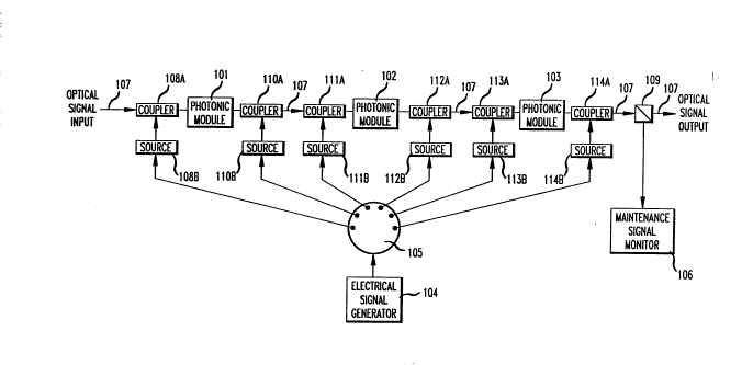
FIG. 1 is a cimrlifiecl block diagram showing an optical co....n~nicq-tiQn
system inco,~,~ting a particular emwiment of this invention. As shown, three
photonic modllles (101, 102, and 103), rlectrirAl signal g~ alO~ 104, clc~ !- ;cAl
signal co.. ll~. 105"~in~nAI~ce signal ,n- ni~r 106, and opdcal tr~ncmi~sjQn
line 107 are included in the system. A primary h~fc.... AI;-.n bearing optical signal is
1 along opdcal llnnc~;ssjon line 107 from input to output. In practiCing
the invention, a m~lllAted analog n.~;nle--An~e signal is i~jeclcd into the optical
signal traveling along optical trAncmiccion line 107, prior to the input of photoni~
20 module 101. This mod~llAte~ signal is produced by optical source 108b and injected
via coupler 108a. Optical source 108b produces the modlllAted optical signal in
respo~se to an analog e1ectri< ~l signal produced by e1ectricA.1 signal genel~alol 104,
and dil~l~;d to opdcal source 108b via elestricA1 signal distlibutor 105. As theinjected ms~1lllAted opdcal signal prop~tes along opdcal mAncmiS~iQn line 107
25 toward the opdcal signal output, it passes through opdcal tap 109. Opdcal tap 109
routes a pordon of the mo~lllAtPcl signal to ...Aint~ ~A'~ce signal Illonilol 106.
~Ai~lt~ nce signal ~--onilor 106 analyzes the received optical signal and d~ ---in~s
if the mod~1lAted signal illje~ l~d at coupler 108a has been s~lccescfully trAnemitted
through the opdcal co....n~n;c~t on system.
Another en~oded .nAinten~nce signal is then injected by coupler 110a
into the primary opdcal signal traveling along optical trAnsmicsion line 107
following the output of photonic module 101. This .nAintenAnce signal is genel~led
by optical source 110b in response to an analog electrical signal pl~luc~l by
electrical signal ge.-e.i ~OI 104, and directed to optical source 110b via e1ectri
35 signal distributor 105. The resultAnt mo~3nlAted opdcal signal propagates along
optical trAnsmi~sion line 107 toward the opdcal signal output. As the m~dulAtrd
20961Sl
- 4 -
signal passes through optical tap 109, a portion of the signal is routed to .,.~ t~ -~nce
signal n~or ;lor 106. ~inten~nre signal monitor 106 analyzes the received optical
signal and delc ...ines if the mod~ tç~l signal inll~luced at coupler 110a has been
succe-ssfully lli.n~ ;d through the optical co~ unic~tion system.
S If .~;nt~nsnce signal ~.~oni~or 106 s~lcces~rully receives the
-hE nance signals inl~uduce~ at both coupler 108a and coupler 110b, photonic
module 101 is ~u~-~ed to be OpC~ati~lg plo~.ly. Lf, hu..~ ,r, ~ ;n~n~nce signal
l~lonilor 106 receives the signal injected at coupler 110a, but fails to receive the
signal injected at coupler 108a, photoni~ module 101 would be cqn~i~çred faulty.The above clessribed tesdng ~luc~lul~ can be applied to photonic
m~lles 102 and 103 (employing opdcal sources/couplers 11 la/b and 112alb for
pho~c~nic module 102, and optical sources/couplers 113alb and 114alb for photonic
module 103), so as to ~lete..nil-e if these m~lnlçs are faulty. The same ~ C~
can be used to check the integrity of opdcal tr~n~mi~sion line 107 as well (by
15 employingcoupler/sourcepairs 110a/b, llla/b, 112alb, 113alb,and 114a/b). The
ele~tric~l signal provided tû a pardcular opdcal source by electnc~l signal generator
104 may be mn~ te~1 in a manner which ~listin~lishes that source from all others~tt~hed to the optical co~ n~nir~tion system. This may be ~ccon~ hed by pre-
progr~mming electric~l signal gen~.~tol 104 to employ a unique modul~tion pattern
20 or frequency for each of the sources within the co~ ni~tion system.
FIG. 2 is a ~implifie~ biock diagram showing an opdcal co~ ni~qtion
system incorporating a pardcular emlx)~limpnt of this invendon. As shown, three
photonic m~ul~s (101, 102, and 103), two opdcal couplers (201, and 202), two
inter-module opdcal light sources (203 and 204), electrical signal ~.-~ o~ 104,
25 electrical signal ~ trib~tQr 105, .~ nte~n~e signal ...oni~o~ 106, and optical
tr~n~mi~siQn line 107 are included in the system. A primary inf4~ ;011 bearingopdcal signal is t~ ed along opdcal tr~n~m~ n line 107 from input to outpu~
In practicing the invendon, a ~ inl~ n~llce signal is mod~ ted onto the opdcal signal
traveling along opdcal tr~n~mi~ion line 107, prior to the input of photonic module
30 101. This opdcal modlll~tion is accomrlished by opdcal m~ul~tor 205 which
controllably attenll~tes or amplifies the primary i~ tiQn bearing signal traveling
along tr~nsmi~siQn line 107. Opdcal modul~tor 205 is controlled by an electricalsignal which is produced by electlic~l signal ge.le.~lor 104, and directed to opdcal
m~ul~tor 205 via electrical signal distributor 105. As the mod~ te~ optical signal
35 propagates along optical tr~n~mission line 107 toward the optical signal output, it
passes through opdcal tap 109. Optical tap 109 routes a portion of the m~lll~ted
2096151
signal to .~ nlenanre signal ...oniloi 106. l~-a-in~ nce signal .nrJI.;l~ 106 analyzes
the ~ ;v~d optical signal and d~ t~ - ...;n~s if the mo~ ated signal introduced at
- optical mo~ulatnr 205 has been suGcescfully ~ snnlt~ through the optical
co.... ~ n;r~tion system.
S Another enro~ed .. ~in~enqnre signal is then mn~lllat~A by optical
m~i-lla,tor 206 onto the optical signal traveling along optical trancmiccio~ line 107
following the output of photonic module 101. This ~ n~e ~qnl e signal is ~.~rl;.le~
in .e,,~l-~c to an analog elçctrical signal produced by electrical signal ge. ~ ~r 104,
and directed to optical m~~ tor 206 via electrir~l signal ~lictributQr 105. The
10 res~lt~nt modlll~ted optical signal propagates along optical tr~ncmission line 107
toward the optical signal output. As the mrx~ ted signal passes through optical tap
109, a portion of the signal is routed to n~int~ nce signal ~ nito~ 106.
en~nce signal monitor 106 analyzes the received optical signal and ~ t~ ~--;nes
if the tnrxllllated signal introduced at optical ~o~ tQr 206 has been suçcessfully
15 ll~nc~n;l~ed through the optical con~ n~ir~tion system.
If .~ nty-n~nce signal .~o~ 106 succes~rully ,~ce.~es the
n~in~en~nre signals introduced at both optical m~nl~tnr 205 and optical m.~dlll~tor
206, photonic module 101 is ~csumed to be o~.~ g plu~lly. If, ho~
inlf nAnce~ signal ~ n;lol 106 receives the m~lulAteA signal introduced at optical
20 modlll~tor 206, but fails to receive the m~1ul~ted signal introduced at optical
m~lnlA~or 205, photonic module 101 would be c-:?n~idçred faulty.
By employing optical modlll~tors 207, 208, 209 and 210 the above
desçrihe~l testing p,ocedu~ can be applied to phQtQnic mot~ çs 102 and 103 so as to
dete. ,,~ine if these modllles are faulty. The elpctricAl signal provided to a particular
25 optical modul~tor by electricAl signal generator 104 may be m~dul~ted in a manner
which ~ tin~liches that optical modlllA~I~r rom all others flttA~hed to the optical
con-.-. ~;c-~;on system. This may be accomrli~h~ by pre-pro~ ..~-~nh~g electr
signal ~.~--e-nlor 104 to employ a unique modul~tion pattern or enroded ~ uency
for each of the optical modlllAtors within the co~ nir~hon system.
In the event of a severe line fault which prohi~ite~ t-h-e optical input
signal from proFAg~hng to ~~ n~f~Ance l ~n;~J~ 106, inter- module light sources 203
and 204 can be employed to aid in locating the fault. Upon de~ AIion that
"~Ainh~Ance l.~n;lor 106 was not receiving the optical input signal, light from inter-
module light source 203 is injected into tr~n~mission line 107 via optical coupler
35 201. A m~int~nAnce signal is then mod~ ted onto this injected light by mo~llllAtor
207. Lf .~Ain~ nre signal nu~nilor 106 succes~fully receives the n~ Ance signal
209~151
- 6-
introduced by modnlAtor 207, the fault can be ~c ~v~ d to be located in a portion of
trancmicsion line 107 prior to optical coupler 201, or within photonic module 101 or
modulAtors 205 or 206. If the light inie/cted by inter-module optical source 203 fails
to proFags-te to "~int~.~9n~fJ ~ itm 106, light is inject~ at optical coupler 202 by
S inter-module light source 204. MQd~ s~tor 209 msdlllst~s a .~Ainh l~ncfJ signal onto
this injecled light. If .~A;n~ellAnce signal n-oni~o~ 106 ~ccep~rully rtceives this
~~A~ f--~A~ce signal, the fault is Acsllmçd to be in a portion of the co~ fi~Ation
system located ~~ optical couplers 201 and 202. If the light injected at opticalcoupler 202 fails to propagate to ms,intenance ,~oni~Qr 106, the fault is located
10 ~I~._en coupler 202 and optical tap 109.
Another ~.efe.l~d technique of praçti~ing the invention is facilitated by
the co~ nicstionc system shown in FIG. 3. As shown, three photonic modlllçs
(301, 302, and 303), electrical signal gençr~s~tor 304, electnc-sl signal distributor 305,
."Ai~,t~.~Anre signal ,..o~ " 306, and optical trsncmicsion paths 307, 309, 310, and
15 311 are included in the system. E~ill~ y infc~ A,l ;on bearing optical signals travel
along these optical trAncmicsiQn paths from input to output. The photonic m~llles
within this system are each opto- ele~ onic inte~tell guided-wave switching
devices of the typc shown in FIG. 4. The optical ~vilclling within such guided-wave
devices is controlled by the applying voltages to control elecl.odes internal to the
20 devices. Such swilching devices (e.g., directionAl couplers) are typically fahric~te~
from lithium-niobate, and are well know-n in the art.
FIG. 4 shows, in cimplified form, the internAl architecture of photonic
module 301 of nG. 3. Photonic module 301 (a 4 x 4 switch) accepts optical input
signals from optical tranc-micsil~n paths via input lines 401, 402, 403, and 404, and
25 outputs optical signals via lines 405-408. TrAnc-mic-cion path 307 is col-l-e~lçd to
photonic module 301 via input line 401. A switch point having a control electrode is
ACS(xi~t~ with each of the input and output lines in photonic module 301.
~A/litionsl control ele~,~odes are also associat~l with the sixteen int~ ,1;Ate
optical switch points within photonic module 301. A detpilp~ depiction of switch30 point 409 (which is asso.;ialed with input line 401) is shown in FIG. 4. A voltage
applied to el~lludc 410 reglllAtçs the trAncmiccion of optical signals through switch
point 409. The trAnsmicc7ion of optical signals at each input and output can be
similArly regulated by applying a voltage to the AcsociAted control clecll~de. Each of
the control electrodes Acsoci~ted with an input or output line within photonic module
35 301 is CO~ f cled to electricAI signal ~;ene.ato~ 304 via electric~l signal distributor
305. Photonic m~nles 302 and 303 are each configured similarly, and the control
2096151
-- 7 --
el~l,odes ascoci~teA. with the input and output lines of these photonic modllles are
similarly col-nect~d to electric~l signal generator 304.
In l,l~ing the invention within the optical co.-~.. ni~ation system of
FIG. 3, an encoded ...~inlen~ e signal is mo~ teA onto the optical signals
S traveling along optical tr~ncmis~iQn path 307 at the input of photonic module 301.
This optical mn~ tion is accQmrliched by tran~ g modlll~teA voltages to
control electrode 410 (FIG. 4) from ele,ctric~l signal gen~,-dtO~ 304 (FIG. 3). In
ol~ce to these m~xllll~ted voltages, control ele.,llode 410 causes the optical signal
being tï~ncmitteA along path 307, and entering photonic module 301 via input line
10 401 to be mo.1lll~teA The switch points within photonic module 301 are biased to
allow the mod~ teA. optical signal to exit photonic module 301 at output line 405.
The m~~ ted signal prop~gates along optical tr~ncmiccion path 309. The switch
points within photonic module 302 and photonic module 303 are biased so that them- dlllat~A. signal on tr~mmission path 309 is propagateA. to tr~n~micsi~n lines 310
15 and 311, and optical tap 308. Optical tap 308 routes a portion of the modlll~teA,
signal to ...~h~le.~n~e signal monilor 306. ~int~A~ce signal ...onilor 306 analyzes
the received optical signal and ~letermines if the m~~ teA, signal introduced at the
input of photonic module 301 has been ~.lcces~l'ully tr~n~n;l~d through the optical
co--.... .....-ir~tion system.
Another encodeA~ m~int~n~nce signal is then m~lnl~te~ onto the optdcal
signals traveling along opdcal tr~n~mission path 307 at switch point 411 (FIG. 4) of
photonic module 301. This opdcal m~1lll~tilm pe rO- - - -~ in respo~,~e to a
m~ t~A voltage produced by çlectric~l signal g. .~ lo. 304, and directed to the
control el~,ode within switch point 411. This control ele.i~lode lece;~,~s the
25 m~lll~trd voltage from electrical signal gen~.ator 304 via el~tric~l signal
distributor 305. The reSult~nt ,mo~ ted optdcal signal exit~s phot~l-ic module 301
via line 405, propagates along optical tr~n~m~ on path 309. Switch points withinphotonic m~dules 302 and 303 are biased so as to f~cilit~te the tr~n~mi~sion of the
modlll~t~A optical signal along tr~n~mi~c;~n paths 310 and 311 to optdcal tap 308.
30 As the modlll~t~ signal passes through opdcal tap 308, a pordon the signal is routed
to ~--~ n~e signal l--ollitQ 306. ~int~n~nce signal ...~ to~ 306 analyzes the
received optdcal signal and determines if the modlll~çA signal ihlll~luced at the
output of photonic module 301 has been successfully tr~n~mitted through the optical
co.~.. i-ic~tion system.
20961~1
-
- 8 -
If .~s;t~tçnqn~e signal n~onitol 306 succes~fully receives the
"lainten~nce signal introduced at both input 401 and output 405 of photonic module
301, then the paths within photonic mndnles 301, 302, and 303 traversed by the
m~inten~n~e signal are a~sum~l to be ~,Ç5,..-.;ng ~.o~ly. If, however,
5 ,..~h-~en~nce signal ...o~ or 306 receives the mod~ teA. signals rigin~ting at the
output of photoni~ module 301, but fails to receive the m~~ t~A signals l~rigin~ting
at the input of Fhotonic module 301, the path within photonic module 301 would be
co~sidered faulty. ~ltern~tively~ if ~y~a jnle,n~n~e signal mnnitor 306 fails to receive
both the modul~ted signal origin~ting at the input and the output of photonic module
10 301, fault is a~sllmeA. to be "dow"~ a,.." (i.e., within photonic modllles 302 and
303).
The above AescribeA testing procedure can be applied to various
p&lllwdyS within photonic module 301 so that each possible pdlh~a~ through the
module may be ev~ t~A In ~lclitil?n~ the overall plocedul~ can be le~ l for
15 pholonic m~llles 302 and 303 so dS to ~let~,----;n~ if the various pa~-ways within
either of these m~llles are faulty. The input and output lines of each of the pholonic
mC dlll~s shown in nG. 3 may be selectively co,~ ~ to other photQnie modllles
using known ~wilchi..g and control techniques to allow all possi~le ~ h.. à~S
~l~. ce.l the modulçs to be ev~ teA. As is shown in FIG. 3, an optical tap is
20 provided for each output line of photonic module 303 so that each of these output
lines may be .n~ ed by ",~ hn~l~a~ce; signal ...on;tc,r 306.
The rl~ ;c~l signal provided to a particular control ele~llodc within
any of the photonic modules shown in FIG. 3 may be m~ul~tçd in a ~ which
tingl-i~hes that particular control module from all others within the optical
25 co.... ~;~ation system. This may be acc-.. plished by pre-prog~.. ;n~ electric~l
signal gene~ 304 to employ a unique mo~ ti~n pattern or frequency for each of
the m~~ tors within the co~ nication system.
By employing the pre-existing control electrodes within the opto-
electronic integrated guided-wave swilclling devices to pc.ro..-- the ".Ail,t~ ~Qnce
30 signal modlll~ti~n, the need for external ~ nlJAIrJ-s or modlll~t~rs is elimin~te(1
This reduces the cost of implçmenting such a ~ - ro~ nce ~ol~itc~ g system~ and
removes a ~ iricAIlt source of optical signal losses. The application and practice of
the invention with respect to opto-electronic integrated guided-wave swilchitlg
devices is not limited to those f~bri~ated from lithium-niobate. It may be practiced
35 with switching devices fabric~te~ from indium-phosphide, as well as other types of
guided-wave s~vilcl.ing devices. In ~ddition, the invention may also be applied to
2096151
free-space optical swilchillg devices by directing the modulA~ed voltages produced
by the electrical signal g~n~,lato~ to the control mechAni~m~ coh~ n~ within these
swilching devices. Furthçrmore, the particular configuration and complexity of the
opto cle~,~o.1ic illte~aled guided-wave swilchillg devices with which this invention
S is practiced is imm~q~tçr~ as long as a control electrode or .nechA~ m is provided
for each optical line ent~rin~ and exiting the device. Note that in the above
described example there is no need to transmit a m~dul~q~te~l voltage to the control
electrodes a~ociAtç~l with the sixteen intr....~Aiq,te optical switch points within
photonic module 301.
One scheme for conpling a signal intenA~l to rnc~lul,q,te a ,~Ah~l~ nAnce
signal to a control electrode within a photonic module is shown in FIG. 5. The
signal (such as one generated by electr~ signal genel~lo~ 304) is input on line 501
and capacitively coupled via cap~itor 502 to ~wilching control line 503. Switching
control line 503 is connecl~ to control ele~ ode 504 within photonic module 505,15 and serves to carry signals (received via inductor 506) which control optical~wilching on line 507. This arrngement permits one col-n~ ;on to carry the signals
which control s.vi~hing and ...Aillt. -A~-ce signal m~llq~ion cim~ eo..cly.
An qltçrnAte scheme for coupling a ".Ail~ nAI~e m~dlllAtion signal to a
control ekcllode within a phot~ni~ module is shown in FIG. 6. The signal (such as
20 one ge.~ t~l by electrir-ql signal ~nc,.~lol 304) is input on line 601 to the gate of
FET 602. Switching control line 603 is conn~cted via the channel of FET 602, to
control electrode 604 within photonic module 605, and serves to carry signals
(received from a switch controller) which regulate switching on line 606. Resistor
607 serves to provide a path to ground so that absent a signal from the switch
25 controller or input line 601, the potential across control electrode 604 is essçntiAlly
zero. Only one col.~-c~ .n is needed to carry the signals controlling both switching
. nd l..q-inlnnA~e signal modulAtion
In any of the above described emhodh~e ~l~ the mo~ lq~ted n~ t~ e
signals may be encodçd to carry such inÇ,..n~l;on as input/output port identity,30 module identity, circuit pack identity, as well as a test pattern dçsignçrl test specific
tr~n~mi~sion ch&l~te- ;~I;cs of particular photonic moflnles and/or tr,qn~mi~si~n
paths. The modlllAted signals could also carry info....-qtio~ related to factorseffecting the general ~. . . ~Ance of the modllles within the co~n~ -----lic~tion system
(i.e., ambient temperature at any given module). The mr~ul~tion employed may be
35 any type (e.g., amplitude shift keying, frequency shift keying, phase shift keying,
etc.), and the sub-carrier fre~uency may be any within practical limits.
2096151
- 10-
The above~esrribe~l invention provides a practical p~.r~ nçe
Illoni~ ing technique which allows faults within an optical co~ nic~tion system
- to be ~l~tçctçd and located. It will be unde.~lood that the particular metho-3s
~esçribe~l are only illustradve of the prinçirles of the present invention, and that
5 various mo~3ifiç~tion~ could be made by those skilled in the art without dep~ g
f~om the scope and spirit of the present invention, which is limited only by theclaims that follow.
One such mo~ifiratiQn would include ~nera~ing the analog e1ç~trir~1
signals provided to the optical sources and m~~ tors in the above ~les~ibe~
10 examples at a plurality of individual elec~ical signal ge~l~tors; each of these
gen~,~a~ being ~leAir~ted to a particular photonic modllle~ photonic module port, or
group of photonic module ports.