Note: Descriptions are shown in the official language in which they were submitted.
WO 92/11554 PCT/GB91/02131
1
INl'BriSIT>< DIVIDING DEVICE
This invention relates to an intensity dividing device for use in division
of radiation.
Radiation intensity dividing devices are known, such as for example
optical fibre Y-junctions. Y-junctions may be symmetrical, for division
of one input beam into two substantially equal intensity beams. Such
devices are discussed by Z Weissman, A Hardy and E Marom in "Mode-
Dependent Radiation Loss in Y Junctions and Directional Couplers", IEEE
Journal of Quantum Electronics, Vol 25, No 6 (1989) pp 1200-1208. Active
symmetric Y-junctions which employ electro-optic effects to achieve
asymmetric splitting are also known. An example is described by H Sasaki
and I Anderson in "Theoretical and Experimental Studies on Active Y-
Junctions in Optical Waveguides", IEEE Journal of Quantum Electronics, Vol
QE-14, No 11 (1978) pp 883-892. However, symmetrical Y-junctions, both
active and passive, suffer from high losses, particularly for split angles
greater than a few degrees.
Asymmetric Y-junctions capable of dividing an input beam into two beams of
differing intensities are also known. One such device is described by x
Shirafuji and S Karazono in "Transmission Characteristics of Optical
Asymmetric Y Junction with a Gap Region", Journal of Lightwave Technology,
Vol 9, No 4 (1991) pp 426-429. Zt is considerably more efficient than
more conventional Y-junctions since it uses total internal reflection to
redirect radiation to one of the two output parts. Radiation reaches the
other output port by coupling across a gap. This radiation is not
deviated from the input direction of propagation. The power splitting
ratio is determined by the width of the gap.
All Y-junctions, however, suffer from the disadvantage that they can only
provide two way splitting. Therefore, to achieve higher order splitting
Y-junctions are used in series, thus multiplying the losses incurred at
each stage.
PCT/G B91 /02131
WO 92/11554
2
Many other forms of intensity dividing device are also known. In
International Patent J~pplication No PCT/US89/00190, published under
International Publication No. WO 89/06813 E xapon describes optical
waveguide junctions. One incorporates a single input waveguide with four
single mode output waveguides of differing widths and/or differing
refractive indices, radiating from an end. The output waveguides are
therefore characterised by different propagation constants. For a given
input wavelength, different modes of the input waveguide will couple to
different output waveguides, as a result of the different propagation
constants. However, this is an inefficient device with high transmission
losses, since energy from each mode will in general enter each output
waveguide but will be lost from those with unfavourable propagation
constants.
An alternative device described by E Kapon incorporates four single mode
input waveguides of differing widths and/or refractive indices, converging
into an area from which three single mode output waveguides radiate. The
modes excited in the cosson area are dependent on which input waveguides
are providing radiation beams. The output waveguides operate as described
for the single input devices. These devices enable radiation to be
divided according to the ratio of excitation of modes in the waveguides
feeding the output waveguides. However, as previously stated they are
highly inefficient.
1n US Patent 4,693,546 J P Lorenzo and R 1~ Soref describe a "Guided Wave
Optical Power Divider". It is in the form of an X-junction. Two input
waveguides converge on an input end of a crossover region and two output
waveguides diverge from an output end of the region. The input and output
waveguides are single mode and of width W. The crossover region supports
two modes, one odd and one even, and is of width 2W. The device is formed
from crystalline silicon and the crossover region is doped. In an undoped
device radiation passes through the crossover region substantially
undeviated, and enters the first output waveguide. In a doped device
waveguide modes are perturbed and a fraction of the input radiation is
deviated whilst passing through the crossover region and enters the second
output waveguide. The proportion of light deviated is determined by the
WO 92/11554 3 ~ ~ ~ ~ ~~ ~ PCT/GB91/02131
level of doping and may be in the range 10 to 20~. Lorenzo and Soref do
not mention the losses suffered in these devices, other than to state that
the addition of dopants increases absorption by a small amount.
In order to produce more cooplex devices a number of the X-junctions are
combined. They may, for instance, be used to fore a predetermined optical
signal distribution network. However, such networks are quite complex,
for even a modest number of inputs and outputs.
Another form of intensity dividing device is described by A Mahapatra and
J h Connors in European Patent Application 88108258.0, Publication
No 0 301 194. The devices described incorporate one or more input
channels, and a number of output channels, provided on opposite sides of
a planar waveguide. Essentially, radiation input to the planar waveguide
fans out and is thus incident on apertures of the output waveguides. The
patent application describes how the devices may be constructed to improve
uniformity of coupling. That is to obtain substantially equal intensity
in each of the output wavegufdes. These devices will be inherently
inefficient, since much of the radiation input to the planar waveguide
will be incident on portions of waveguide wall between output waveguide
apertures. As a result it will either be absorbed or reflected back to
interfere with radiation in the planar waveguide.
Yet another form of device is described by T P Young and I R Croston in UK
Patent Application 2 215 482A, which is entitled "Optical In-line filter".
It incorporates a first multimode waveguide whose output end is coupled to
an open end of a second, narrower waveguide. The coupling and the length
of the first waveguide being such that light entering the first waveguide
undergoes interference between at least two of its modes. This causes
light from the first waveguide of a predetermined waveband, or wavebands,
only to enter the second waveguide. Light of other wavebands is provided
with alternative means by which it may leave the first waveguide. Thus
the device is capable of separating one waveband (or a set of harmonic
wavebands) from others using modal dispersion. It thereby divides the
intensity of the input radiation, but that is purely a by-product of the
purpose of the device, the proportions of power in the various output
WO 92/11554 ~ ~ ~ ~ 4 ~ '~ PCT/GB91/02131
4
beams are determined by the proportions of different wavelengths in the
input beam. There is no means by which the contribution from one
wavelength may be divided.
1~ further form of waveguide intensity dividing device using modal
dispersion is described in UR Patent No 1 525 492 entitled "Self Imaging
System Using a Waveguide". This describes many different devices using
multimode waveguides supporting at least fifty modes. Figure 33(a)
illustrates a device for dividing a single input image into a number of
identical images of differing intensities. 1~n input waveguide feeds an
image into a first rectangular waveguide, of width eZ and length L.
large number of modes are excited in the first rectangular waveguide,
modal dispersion occurs and after a length L five images, each
substantially one fifth the intensity of the input image, are produced.
t5 Three of the five images pass to a second rectangular waveguide of width
and length L', whilst the remaining two pass to a third rectangular
waveguide of width e=" and length L". Modal dispersion also occurs in the
second and third rectangular waveguides. Thus after a length L' the three
images are recombined. Likewise after a length L" the two images are
recombined. The second and third rectangular waveguides each feed an
output waveguide of like dimensions to the input waveguide. The images
entering these waveguides have intensities in the ratio 3:2.
The device described in Uic Patent No 1,525,492 is more efficient than
previously described prior art devices. However it suffers from a number
of disadvantages. It requires waveguides capable of supporting a large
number of modes, and these are difficult to produce. In addition it is
fairly complex, and inconveniently long for many applications.
It is an object of the invention to provide an alternative intensity
dividing device capable of producing a set of different intensity outputs
fros input radiation.
P~1~ '~ 2 ~ 0 2131'
2996 X22 ~ 5 l5 FEBR
U~RY 1993
The present invention provides an intensity dividing wherein:-
(A) the device includes:
(a) a multimode waveguide,
(b) at le,3st one input port arranged to relay input
radiation of a single wavelength to excite both
symmetric and antisymmetric modes of the multimode
waveguide, and
(c) a set of output ports which are spaced apart across
a transverse section of the multimode waveguide; and
(B) the multimode waveguide and the input and output ports have
geometries and a spatial relationship therebetween which are
in combination arranged such that input radiation
propagating as a fundamental mode to the multimode waveguide
would, due to modal dispersion, produce intensity
distribution maxima of differing magnitude at respective
output ports, each maximum being substantially a reproduction
of the input radiation fundamental mode.
The invention provides the advantage that it provides radiation division
into unequal intensity outputs, and is capable of high efficiency if
correctly made. It is applicable inter alia to light beating equipment
requiring a low intensity beam for use as a local oscillator and a high
intensity beam for output to and backscattering or reflection from a
sample or region under investigation.
The invention may incorporate a set of input ports, and the input and
output ports may be connected to input and output waveguides respectively.
The input waveguides may contain phase shifters, and be arranged to
receive like intensity radiation. In this case, the phase shifters are
controllable to vary intensity levels received by respective output
waveguides.
United Kingdom Patent Office
PCT International Application
PCT/GB91 /02131
WO 92/ 11554
2 6
The invention may include a second eultiaode waveguide with associated
input and output ports, this waveguide being arranged in series with the
multimode waveguide referred to above. In this case, the two multimode
waveguides are arranged to apply two successive stages of selectable
intensity division to radiation propagating between a device input and a
device output.
In order that the invention might be more fully understood, embodiments
thereof will now be described, by way of example only, with reference to
the accompanying drawings, in which:-
Figures 1 and 2 are respectively horizontal and vertical sectional
views of an intensity dividing device of the invention;
Figure 3 shows modal amplitude distributions for various lower order
waveguide modes;
Figure 1 illustrates changes in transverse electric field intensity
distribution with distance along a aultimode waveguide;
Figure 5 illustrates changes in transverse electric field intensity
distribution with distance along a multimode waveguide, for division
of a single input into H maxiaa, where N is (a) 6, (b) 5, (c) 4,
(d) 3 and (e) 2;
Figure 6 illustrates changes in transverse electric field intensity
distribution with distance along a multimode waveguide, for division
of a single input into 6 aaxima, where each of (a) to (f)
corresponds to a different input location;
Figure 7 is a schematic sectional plan view of an electro-optically
programmable device of the invention;
Figure 8 is a schematic sectional plan view of a device of the
invention incorporating cascaded, transversely movable multimode
waveguides; and
WO 92/11554 ~ ~ ~ ~ ~ ~ ~ PCT/GB91/02131
7
Figure 9 is a scheaatic drawing of a device of the invention
incorporated in a laser vibrometer.
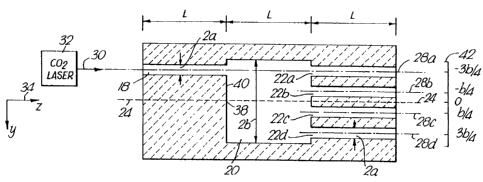
Referring to Figures 1 and 2, an intensity dividing device of the
invention indicated generally by 10 is shown in a sectional plan view and
a sectional side view respectively. It is in the form of a beamsplitter,
and it incorporates three layers or strata 12, 14 and 16. The strata 12
to 16 are lower, central and upper layers respectively. The lower and
upper layers 12 and 16 are continuous sheets of alumina. The central
layer 14 is a sheet of like material which has been Billed to provide
slots through its thickness. Slot sides so formed provide waveguide
sidewalls. The lower and upper sheets provide lower and upper waveguide
walls.
Figure 1 is a horizontal section through the central layer 14 parallel to
its surfaces 14a and 14b. The slotting defines an input waveguide 18, a
beamsplitting waveguide 20 and a set of four output waveguides 22a to 22d
(referred to collectively as 22).
The beamsplitter 10 has a central longitudinal axis 24 (dotted line), and
the output waveguides 22 have respective longitudinal axes 28a to 28d
(chain lines). The axes 24 and 28 are coplanar and parallel. In Figure
2, the axes appear superimposed, the latter being referred to collectively
as 28.
The input waveguide 18 is coaxial (axis 28a) with an outermost output
waveguide 22a. it receives input radiation 30 of 10.59 um wavelength from
a C02 laser 32. The laser 32 is focussed to a beam waist of diameter
equal to 1.42a between 1/e2 intensity points. The beam waist is located
at the centre of the left hand (input) end of the input waveguide 18. The
laser beam waist profile in planes perpendicular to the axis 24 is
Gaussian.
The input and output waveguides 18 and 22 are all of square transverse
cross-section with side 2a. The beamsplitting waveguide 20 is of height
2a and width 2b. The parameters a and b are employed to preserve
WO 92/11554 ~~ ~ ~ ~ PGT/GB91/02131
8
generality and assist mathematical analysis. in one embodiment of the
invention, 2a = 1 mm and 2b = 8a = 4mm. The waveguides 18, 20 and 22 are
each of length L, given by:-
L = 2nb2/~o (1)
where: n = refractive index of waveguide core material, ie. air in
the waveguides 12, 20 and 22;
b - beamsplitting waveguide half width as defined above, and
~10 = free space operating wavelength = 10.59 um for the C02
laser 32.
Alternatively, replacing n/x0 by .1, the operating wavelength in the
beamsplitting waveguide, Equation (1) becomes:-
L - 2b2/J1 (2)
with 2b = 4 mm and a = 10.59 um, L = 755 mm. It should, however, be noted
that the lengths of waveguides 18 and 22 are not of great significance to
the operation of the device 10. They were chosen to be of length L purely
for simplicity of description and construction.
Coordinate axes 34 and 36 are shown in Figures 1 and 2 respectively, these
defining yz (horizontal) and xz (vertical) planes. The z axis is the
central longitudinal axis 24; x, y and z are defined as zero at 38 where
the axis 24 intersects a left hand transverse wall 40 of the beamsplitting
waveguide 20.
The locations of the waveguide axes 28, ie their offsets in the y
direction with respect to the z axis 38, are shown on a scale 42. The
axes 28a to 28d have y coordinates -3b/4, -b/4, +b/4 and +3b/4
respectively. The beamsplitting waveguide 20 may be notionally treated as
divided longitudinally into quarters bounded by axes (not shown) with y
coordinates -b, -b/2; -b/2, 0; 0, +b/2; and +b/2, +b. The axes 28 are
WO 92/11554 ~ ~ 4 ~ ~ PCT/GB91/02131
9
therefore located periodically in space across the horizontal transverse
y dimension of the beamsplitting waveguide 20. They are located centrallv
of respective waveguide quarters. In general, and in accordance with the
invention, it can be shown that input and output waveguides, ie coupling
waveguides, should have axes located centrally of respective equal
subdivisions of the beamsplitting waveguide's transverse cross-section.
In a device of the invention having N output guides, the latter would be
located centrally of respective beamsplitting waveguide cross-sectional
Nths.
The theoretical propagation characteristics of a rectangular waveguide
will now be briefly analysed. It is assumed that the waveauide has height
2a, width 2b and is bounded by a hooogeneous dielectric material with
complex dielectric constant E. It is also assumed that this dielectric
material (which provides the waveguide walls) is highly reflecting and not
significantly attenuating for required propagating modes. The waveguide
has height, width and length dimensions which are parallel to the x, y and
z axes respectively. It has normalised linearly polarized modes of the
kind EH~. The electric field contribution E~(x,y,z) of the ninth mode
Et~ at the point (x,y,z) has been calculated by Laakmann et al in ~ppl.
Opt. Vol. 15, No. 5, pages 1334-1340, Ilay 1976 as follows:
Emn( x~ Y. z ) = 1 [cos m~ cos nrty eiY~z ( 3 )
(ab) lsin (~~,[sin (~,,
where
m is the mode number relating to the field dependency along the x
axis,
n is the mode number relating to the field dependency along the y
axis,
z is the distance along the z axis,
1r~ _ (S~ ~ ia~), the propagation constant of the mnthe mode,
and a~ being the mnthe mode's phase and attenuation coefficients,
and
PCTI68 ~ 1 l 0 2131
~0~~
15 EtB~iuAK~ v~~
"cos" above "sin" indicates the former applies to odd mode numbers
(m or n as appropiate) and the latter to even mode numbers.
The phase coefficient ~~ is given by:-
5 ~
amn - -~[1 ~~ ~a~2 + ~~b~2~~ (4.1 )
If the negative term in parenthesis in Equation (4.1) is small compared
with unity (paraxial radiation approximation), which is satisfied in
10 practice, then the binomial theorem may be used to rewrite Equation (4.1)
as:-
amn = ~[1 ~~~~a~2 + ~~b~2~~ (4.2)
where a, b, m and n are as previously defined, and l is the free space
wavelength of the radiation propagating in the waveguide.
Equation (3) sets out the electric field contributions obtainable from all
linearly polarized modes of a rectangular waveguide. It is calculates on
the basis that the electric field contribution of each mode is zero at the
side walls of the waveguide, ie at y = +b and -b, where y = 0 on the
axis 24. This is satisfied if the central waveguide has reflecting side
walls. Not all central waveguide modes are necessarily excited by a given
input. In the case of the device 10 of Figures 1 and 2, the heights of
the input and beamsplitting waveguides 18 and 20 are matched and equal to
2a. The input waveguide 18 supplies an excitation in the form of its
fundamental or lowest order mode EH11. This is coupled to the various
EH~ modes of the rectangular beamsplitting guide 20. The input EH11 mode
consequently becomes decomposed into a linear combination of the EH~
modes with respective complex multiplicative coefficients Ate. This is
expressed by:-
EH 1 1 = ~ A~ . EH~ ( 5 )
Essentially the A~ amplitude coupling coefficients are the coefficients
of a Fourier series which represents the field passing from the input
United Kingdom Patent Office SUBSTITUT:~ S~E~
Dr'T Infnrrv~iinn~l ~nn~il~atfnrl
WO 92/11554 11 ~ ~ 9 ~ (~ ~ ~" PCT/GB91/02131
waveguide into the beaasplitting waveguide 20. The EH~ modes are
mutually orthogonal, and in consequence the coefficients 1~ can be
calculated from overlap integrals of the fore:
tb ~a
j EH 1 1 . EH~ . dy . dx . ( 6 )
-a
The forms of some of the lower order EH~ waveguide modes are shown as
electric field amplitude distributions in Figure 3. These were obtained
by computation, and are shown as graphs 1~ to F in quasi-three dimensional
form. The coordinate axes are shown at G. The axes x, y and z
correspond to transverse vertical, transverse horizontal and longitudinal
directions in the multimode waveguide 20 as before. The graphs 1~ to F
correspond to modes as follows:-
J~ : EH11; H : EH21; C : EH31%
D : EH12; E : EH13; F : EH22.
Of these, ~, C and E are symmetric modes and B, D and F are antisymmetric
modes. To clarify this, let E(x) and E(-x) respectively be the
electrical field amplitude distributions associated respectively with
positive and negative parts of the x axis in Figure t; E(x = 0) is on the
z axis 24. Let E(y) and E(-y) be the equivalents for the y axis.
For a symmetric mode:-
E(x) = E(-x) and E(y) = E(-y) ~ (7.1)
For an antisymmetric mode, either one of or both of (7.2) and (7.3) below
apply:-
E(x) _ -E(-x) (7.2)
E(Y) - -E(-Y) ~ (7.3)
WO 92/11554 ~ ~ ~ ~ PCT/GB91/02131
12
In the device 10, the fundasental mode input offset from the axis 24
provides for symmetric and antisymmetric modes of the multimode waveguide
to be excited.
The transverse electric field distribution in an xy plane distant z from
the input to the rectangular waveguide is Ez given by:-
Ez = ~ A~ . EH~ ( B )
The field intensity distribution IZ in xy planes distant z from the input
to the rectangular waveguide is ~Ez~2, the square of the modulus or
magnitude in Equation (8).
Referring now to Figure 4, there is shown a family of graphs of electric
field intensity Iz(y) as a function of y calculated for a multimode
waveguide (not shown) of length 8L. This waveguide has like cross-section
to that of the besmsplitting waveguide 20. Coordinate axes 50, a z axis
scale 52 and y axis scales 54 and 56 indicate the waveguide disposition,
and are rotated with respect to those in Figure 1. The location z = 0 and
y = 0 occurs at a point equivalent to 38 in Figure 1, ie. where a
longitudinal waveguide axis intersects a waveguide wall associated with an
input waveguide. The graphs appear at intervals L/2 apart on the z axis,
eg graphs 58 and 60 at z = 0 and z = L respectively.
For clarity, the graph 60 is reproduced at the upper left of Figure 4. It
has four maxima 60a (just discernable), 60b, 60c and 60d with relative
magnitudes (intensities) 1, 4, 12 and 17 respectively, these being centred
on y values - 3b/4, -b/4, +b/4 and +3b/4. Between these maxima Iz(y) goes
to zero.
The graph 58 consists of a single maximum 58a centred at y = -3b/4 and
zero values away from this maximum.
The intensity dividing device 10 operates as follows. The Gaussian
profile laser beam waist at the left hand end of the input waveguide 18
excites the fundamental mode EH11 of this waveguide. Very little of the
PCT/GB91 /02131
WO 92/11554
13
laser radiation appears in higher order modes of the input waveguide 18.
The division of the radiation intensities guided in various modes of the
waveguide 18 are approximately EH11 98~, others 2~. In consequence,
substantially only the fundamental EH11 mode of the input waveguide 18 is
excited. This passes along the input waveguide 18, and produces an in-
phase, half-cycle sinusoidal intensity distribution in the plane of the
left hand waveguide wall 40. It is equivalent in shape, phase and
location to the maximum 58a in Figure 4. It excites symmetric and
antisymmetric modes EH~ (m = 1, n = 1, 2 ...) of the beamsplitting
waveguide 20, which operates multimode in the transverse horizontal y
dimension. The latter operates in lowest (m = 1) mode in the transverse
vertical x dimension, since it is matched in size to the height of the
input waveguide 18 supporting this mode.
The modes EHIn (n = t, 2, 3 ...) propagate at different rates along the
beamsplitting waveguide 20, ie modal dispersion occurs. In consequence,
their phases vary relative to one another giving rise to interference.
This produces variation in Iz(y), as illustrated for a longer waveguide in
figure 4. At z - L in the beamsplitting waveguide 20, intensity
distributions equivalent to maxiaa 60a to 60d are produced. These
intensity distributions are centred on the axes 28a to 28d respectively,
and are located at the left hand ends of associated output waveguides 22a
to 22d. They excite the fundamental modes EH11 of the output waveguides
22, higher order modes being of negligible intensity. This produces
relative intensities 1, 8, 17 and 24 at the right hand ends of the output
waveguides 22a to 22d respectively. Expressing these relative
intensities as percentages, the radiation intensity division is
approximately 24, 16~, 34~t and 48~.
The intensity dividing device 10 consequently produces radiation division
into a range of differing intensity outputs which are spatially separated.
It therefore provides a choice of beam intensities without the need to
employ a variable optical attenuator. It is particularly relevant to
heterodyne light beating apparatus; here a low intensity light beam is
required as a local oscillator signal. l~ high intensity light beam is
PCT/G B91 /02131
WO 92/11554
14
also required for output to a test region, for subsequent reflection or
scattering.
The device 10 offers a significant advantage over the prior art in that it
requires relatively few modes to be supported in the rectangular waveguide
20. In particular the field distribution illustrated in Figure 4 is
substantially fully described by the seven lowest order EH modes, EH11 to
EH1~. Thus the device 10 will operate satisfactorily, as described above,
provided the seven lowest order EHIn modes are supported by the waveguide
20.
To obtain light beam division into further numbers of intensities, the
beams output from the output waveguides 22 may be selectively recombined.
Moreover, these beams may be further divided by cascading a plurality of
devices 10 connected in series.
Referring to Figure 4 once more, further graphs 62, 64 and 66 are shown at
z values 3L, 5L and 7L respectively. These have respective maxima (eg.
62a) of like intensity to those of the graph 60, but arranged in differing
orders along the respective graphs. As before, they are located at y
values -3b/4, -b/4, ~b/4 and ~3b/4. Por example, the aaxima of graph 66
are in inverse order compared to those of graph 60. This demonstrates
that the order of maxima of differing intensities varies with distance z
along a multimode waveguide employed in accordance with the invention. It
can also be shown that the locations of these intensity distribution
maxima along the y axis is variable by altering the position of the input
maximum 58a. In particular, relocating the maximum 58a to a y value
of -b/4, ~b/4 or ~3b/4 would produce similar effects to those shown in
figure 3, but maxima (eg 62a, 66a) on graphs 60 to 66 would be rearranged
in position. These positions would still be at respective y values
selected from -3b/4, -b/4, ~b/4 and ~3b/4 and at z values L, 3L, 5L and
7L. In consequence, the positions of intensity maxima such as 60a on the
graph 60 ( z = L ) may be altered by changing the location of the input
maximum 58a from a y value of -3b/4 to -b/4, ~b/4 or ~3b/4. The input
maximum 58a is located at the centre of a longitudinal subdivision (one
quarter) of the multimode waveguide. It may be located at the centre of
WO 92/11554 15 ~ ~ ~ ~ ~ ~ ~ PCT/GB91/02131
an Nth subdivision, in which case it will give rise to division into N
maxima at z = L.
Devices similar to the device 10 may be constructed for different orders
of beam division. In particular, if N beams each of different intensity
are required, as in the device 10, then the following criteria may be net.
hirstly the rectangular waveguide should be sufficiently wide for N output
ports to be appropriately located to accept the required output maxima.
That is each output waveguide should be of like cross-section to the input
waveguide and should be located at the centre of an Nth subdivision of the
waveguide width 2b. Secondly the length L, of the beamsplitting waveguide
should be given by:
L ~ 8b2 (9)
Thirdly the input waveguide should be appropriately located. For all
values of N a single fundamental mode input beam may be located at
y = s(N - 1)b/N. For some values of N other input locations may also be
appropriate. Por instance when N = 4, as described earlier there are four
appropriate locations y = :(N - t)b/N and y = t(N - 3)b/N.
Referring now to higure 5, there are shown fasilies of graphs of electric
field intensity Iz(y) as a function of y calculated for a multimode
waveguide, of width 2b = 12a. Each of the families (a) to (e) indicates
division of a single input beam located y = -(N - 1)b/N into N maxima of
different intensities at a length of L - 8b2/NA, for N - 6 to 2
respectively. Cartesian co-ordinates are used as before and relevant axes
are indicated by 80.
In Figure 5(a) (for which N = 6) graph 82 represents an input radiation
beam intensity distribution located at y = -(N - 1)b/N = -5b/6. This
input beam is a fundamental mode beam, and it excites both symmetric and
antisymmetric modes of the rectangular waveguide. As these modes
propagate along the waveguide in the z direction modal dispersion occurs.
After a distance z = 8b2/Na = 4b2/371, the dispersion produces an electric
field distribution incorporating six maxima 84a to 84f (collectively 84)
PCT/GB91 /02131
WO 92/11554
16
located at y values -5b/6, -3b/6, -b/6, +b/6, +3b/6 and +5b/6
respectively. The maxima 84 are each of a different intensity, the
intensities ascending from 84a to 84f, a1s a percentage of input
intensity, and to a first approximation, the intensities of 84a to 84f are
it, 5~, 13~, 2111, 28~ and 31; respectively.
Similarly for N = 5, illustrated in Figure 5(b), a single fundamental mode
input beam located at y = -4b/5 is represented by graph 86. ~t a distance
z = 8b2/5~ five maxima 88a to 88e are produced. They are located at
y = -4b/5, -2b/5, 0, +2b/5 and +4b/5, respectively. To a first
approximation, their intensities, as a percentage of input intensity, are
88a 1~, 88b 8~t, 88c 2011, 88d 32~ and 88e 39~.
Input Output
Figure-
N Via- 5 Figure 5 Intensi-
tion Refer- Locations References ties as
1t
ence of input
intensity
6 -5b/6 82 -5b/6 -3b/6 -b/6 84a to 84f 1, 5, 13,
+b/6 +3b/6 +5b/6 21,28,31.
5 -4b/5 86 -4b/5 -2b/5 0 88a to 88e 1, 8, 20,
+2b/5 +4b/5 32, 39.
4 -3b/4 90 -3b/4 -b/4 92a to 92d 2, 16,
+b/4 +3b/4 34, 48.
3 -2b/2 94 -2b/3 0 +2b/3 96a to 96c 4,33,62,
2 -b/2 98 -b/2 +b/2 100a and 15, 85.
100b
Table 1 Summarv of beam division illustrated in Figure 5
WO 92/11554 ~ ~ ~ ~ 4 ~ ~ PCT/GB91/02131
17
Tha bear division illustrated in Figure 5(a) and (b) is summarised in
Table 1. Details of the beam division for N = 4 to 2, illustrated in
Figure 5(c) to (d), is also given in Table 1.
Referring now to Figure 6, there are shown six families of graphs of
electric field intensity Iz(y) as a function of y calculated for a
multimode waveguide of width 2b = 12a. Each of the families (a) to (f)
illustrates division of a single input bean, located at the centre of an
Nth subdivision of the waveguide width, at a length of L - 8b2/N~l -
t0 4b2/3)1. Cartesian coordinates are used as before and relevant axes are
indicated by 110.
In each of Figures 6(a) to (f) a single fundamental mode input beam is
divided into six maxima located in the z - 4b2/3~1 plane at
y = -5b/6,-3b/6, -b/6, fb/6, :3b/6 and ;5b/6. Figure 6(a) illustrates the
same input beam location, at the centre of a first Nth subdivision, and
beam division as illustrated in Figure 5(a), and features are like
referenced. Figure 6(b) illustrates a fundamental mode input 112, located
at z = 0, y = -3b/6, that is in the centre of a second Nth subdivision.
After a distance z = 4b2/3a six maxima 114a to 114f are produced. The
maxima 114a, 114d and 114e are of one magnitude whilst the maxima 114b,
114c arrd 114f are of a second magnitude.
Figure 6(c) illustrates a fundamental mode input 116 located, in the
centre of a third Nth subdivision, at y - -b/6. After a distance
z = 4b2/3x six maxima 118a to 118f (collectively 118) are produced. The
maxima 118 are each of a different magnitude, these being like to the
magnitudes of the maxima 84, but differently located. The following pairs
of maxima have like magnitudes; 84a, 118c; 84b, 118e; 84c, 118a; 84d,
118f; 84e, 118b and 84f, 118d.
Figures 6(d) to 6(f) illustrate beam division when an input is located in
fourth, fifth and sixth Nth subdivisions respectively. Due to the
symmetry of excitation of the multimode waveguide Figures 6(d) to 6(f) are
mirror images, each about the z-axis, of Figures 6(c), 6(b) and 6(a)
WO 92/11554 2 0 9 6 4 ~ ~ PCT/GB91/02131
18
respectively. They will therefore not be discussed in detail but are
included for completeness.
Figure 6 illustrates that, for N = 6, an input fundamental mode intensity
distribution located at the centre of an Nth subdivision of the multimode
waveguide width will result after a length L = 8b2/Nl in division into N
maxima each located at the centre of an Nth subdivision. The N maxima
will not all be of like magnitude. When the input location is :(N -
1)b2/N.l or tb2/N~ then the N maxima will be of N different magnitudes.
Referring now to Figure 7, there is shown a sectional plan view of a
further embodiment of the invention indicated generally by 140. This
embodiment is an electro-optically controlled intensity varying device.
The device 140 is of alumina in which the following waveguides have been
formed by milling (as described for the device 10):
(i) a square (2a x 2a) transverse section input waveguide 142 of
side 2a;
(ii) a rectangular (2a x 2b) transverse section beamsplitting
waveguide 144 of length L/2;
(iii) four square (2a x 2a) transverse section phase control
waveguides 146a to 1464 (collectively 146) containing
respective electro-optic phase shifters 148a to 148d
(collectively 148);
(iv) an intensity control waveguide 150; and
(v) four square (2a x 2a) transverse section output waveguides
152a to 152d (collectively t52).
l~ppropriate values for 2a and 2b are 1 mm and 4 mm respectively.
The device 140 has a longitudinal axis of symmetry 154, with which the
input, beamsplitting and intensity control waveguides 142, 144 and 150 are
WO 92/11554 ~ ~ ~ ~ ~ PCT/GB91/02131
19
coaxial. Each of the phase control waveguides 146 is coaxial with a
respective one of the output waveguides 152; 1e waveguides 146k and 152k
share a respective common longitudinal symmetry axis 156k, where k = a, b,
c or d. The axes 156a to 156d (collectively 156) are parallel to and
coplanar with the device axis 154, but are offset from it transversely and
horizontally by y values -3b/4, -b/4, ~b/4, ~3b/4 respectively. 1~ set of
axes 158 indicates the y and z directions. The device axis 142 is the z
axis, on which y = 0.
The device 140 operates as follows. A C02 laser (not shown) excites
substantially only the fundamental EtIl1 mode of the input waveguide 142.
This mode propagates to the beamsplitting waveguide 144, where it provides
a coaxial fundamental mode excitation. It can be shown that this
excitation generates only symmetric modes in the beamsplitting waveguide
144. l~s stated before, these modes are EEi~ modes where m is 1 and n is
odd. Because only symmetric modes are excited in the beamsplitting
waveguide 144, it can be shown that four intensity distribution maxima of
equal magnitude are created at this waveguide's right hand end distant L/2
from the input. The maxima are centred on respective ones of the axes
156. They are well defined and separated by zero intensity regions, but
are not of like phase. They excite fundamental modes of respective relay
waveguides 146.
The phase shifters 148 have respective electrodes connected to DC bias
voltage sources (not shown). They apply respective phase shifts to
radiation propagating along respective relay waveguides 146.
Referring now also to Figure 4 once more, there are shown four equal
intensity maxima (with unlike phase) incorporated in graphs 71 at z = 2L
and 73 at z = 6L. These respectively convert to graphs 62 and 66 of
unequal intensity (equivalent to graph 60 with exchanged maxima) at z
values of 3L and 7L. In consequence, four equal intensity maxima with
appropriate phase differences are convertible to four maxima with
differing intensities in a length L of multimode waveguide of 2a x 2b
cross-section.
WO 92/11554 . 2-~ 9 ~ ~ ~ ~ 20 P~/GB91/02131
This phenomenon is implemented in the device 140. l~pplication of a series
of sets of bias voltages to the phase shifters 148 produces a
corresponding series of sets of intensity maxima at the output waveguides
152. Each maximum in a set is centred on a respective output waveguide
152. The sets differ only in that the order of size of their maxima
differ. In figure 4 for example, graphs 60, 62, 64 and 66 have equivalent
but differently ordered maxima such as 60a and 62a. Switching between
bias voltage sets consequently produces electrically controlled switching
of the respective intensities in the output waveguides 152. Moreover,
since the device 140 employs modal dispersion for radiation intensity
division, it is capable of high efficiency. To achieve high efficiency,
the requirement is to provide low loss, accurately made waveguides 142
etc. Phase shifters 148 should be of negligible absorption, and should
have antireflection coatings on longitudinal end surfaces through which
radiation passes.
The output waveguides 152 may be connected to respective optical fibres to
route individual radiation intensities to different regions.
Referring now to figure 8, there is shown a sectional plan view of a
further embodiment of the invention indicated generally by 180. It is an
intensity varying device. The device 180 incorporates a support 182 on
which are mounted an input waveguide 184, first and second beamsplitters
186 and 188, and an output waveguide 190. Of these, the input and output
waveguides 184 and 190 are fixed, and the remainder 186 and 188 are
transversely moveable by respective first, second and third screws 192 and
194. The input and output waveguides 184 and 190 are formed as hollows in
respective alumina blocks 184' and 190'. The output waveguide block 190'
has carbon inserts 191.
The first beamsplitter 186 has four input coupling waveguides 200a to
200d, a bypass coupling waveguide 202 and an output coupling waveguide
204. The input and output coupling waveguides 200a to 200d (referred to
collectively as 200) and the output coupling waveguide 204 are connected
to a first beamsplitter multimode waveguide 206, which has an internal
wall region 208 of graphite.
WO 92/11554 21 ~~~~ ~~~'~~ PCT/GB91/02131
The second beamsplitter 188 has four input waveguides 210a to 210d and
four output waveguides 212a to 212d, these being referred to collectively
as 210 and 212 respectively. It also has a bypass waveguide 214. 7~
second beamsplitter multimode waveguide 216 connects the input and output
waveguides 210 and 212.
The waveguides 200 to 216 inclusive are formed as hollows in the material
of which the beamsplitters 186 and 188 are made. The material is alumina
with, in the case of the first beaasplitter 186, a carbon insert 208 as
has been said.
The waveguides 184, 190, 200, 202, 204, 210, 212 and 214 are straight, and
have square transverse cross-sections with side 2a. They are collectively
referred to as coupling waveguides, and are similar to waveguides 18 and
22 in Figure 1. The multimode waveguides 206 and 216 have rectangular
transverse cross-sections with sides 2a x 2b. They are similar to the
waveguide 20 of Figure 1.
The locations of the waveguides in each set 200, 210 or 212 with respect
to y and z axes 217 are at y values -3b/4, -b/4, ~b/4 and ~3b/4. Here the
z axis is along the centre of the input waveguide 184. Locations in the
movable elements 186, 188 and 190 are seasured from the z axis with the
multimode waveguides 206 and 216 and the output waveguide 190 disposed
symmetrically about that axis. The first beamsplitter output waveguide
204 is located at a y value of ;3b/4. l~s indicated by longitudinal scales
220 and 222, the multimode waveguides 206 and 216 are of length L.
The device 180 operates as follows. The first screw 192 is adjusted to
bring one of the first beamsplitter waveguides 200 and 202 into alignment
With the input waveguide 184. l~s illustrated, waveguide 200d is aligned
in this way. A C02 laser (not shown) is employed to excite the
fundamental mode EH11 of the input waveguide 186. Radiation from the
laser is thereby relayed to whichever of the waveguides 200 and 202 has
been aligned as described. If the bypass waveguide 202 is so aligned,
substantially all of the input radiation is relayed to the second
beaasplitter 188. This ignores minor radiation losses within waveguides
WO 92/ 11554 c~ ~ ('~ :~ ~ 22 PCT/G B91 /02131
or at interfaces 218 between adjacent eleaents. With one of the first
beamsplitter input waveguides 200 so aligned, an intensity distribution
having four aaxima appears on the first multiaode waveguide's right hand
side 206'. The distribution is as in one of graphs 160 to 166 in Figure
4, and which of these is appropriate depends on which of the waveguides
200a to 200d is aligned with the input waveguide 184. Only one of the
intensity maxima is located axially of the first beamsplitter output
waveguide 204, and results in radiation being relayed to the second
beamsplitter 188. The remaining maxima appear against the carbon block
208, which absorbs radiation therefrom.
Operation of the first screw 192 brings successiwe waveguides 200a to 200d
into alignment with the input Waveguide 184. It therefore superimposes
successive maxima (see eg maxima 60a to 60d) of differing intensity on the
first beamsplitter output waveguide 204. The combination of the
beamsplitter 186 and screw 192 therefore acts as an intensity varying
device. It allows for 2~, 16~, 34;, 48~ or 100 of the radiation from the
input waveguide 84 to be relayed to the second beamsplitter 188 (ignoring
intra-waveguide and interfacial losses).
Similar effects are implemented by the second beamsplitter 188, the
operation of which will therefore be described briefly. Alignment of any
one of the waveguides 210 or 214 with the input waveguide 184 (via the
first besmsplitter 186) results in a further stage of division of
radiation into maxima of differing intensity. Since the output waveguide
190 is fixed, operation of the screw 194 to align a second beamsplitter
input waveguide 210 with the input and output waveguides 184 and 190 also
produces alignment of an associated second beamsplitter output waveguide
212. In other words a pair of second beamsplitter input-output waveguides
210k-212k (where k = a, b, c or d) become aligned as described.
Alignment to the second beamsplitter input waveguide 210a is equivalent to
maximum 58a in Figure 4. The associated beamsplitter output waveguide
212a receives an intensity maximum equivalent to 60a, because these are
both located at y values corresponding to -3b/4. In consequence, about 2~
of the radiation intensity input to the second beamsplitter 188 passes to
WO 92/11554 ~ ~ ~, PCT/GB91/02131
23
- the output waveguide 190. 11 siailar reduction in intensity occurs if the
other outer waveguide pair 210d/212d is selected.
If one of the inner beamsplitter input/output waveguide pairs 210b/212b or
210c/212c is selected, the relative intensity reaching the output
waveguide 190 will be 48~.
The intensity reaching the output waveguide 190 will be 48i~ or 2~ of that
input to the second beamsplitter 188 according to which of the waveguides
210b to 210d is selected. Unwanted radiation output from non-selected
waveguides 212 is absorbed in the carbon blocks 191.
The second beamsplitter 188 therefore provides a further intensity
division stage with a choice of 2;, 48>E or 100 (waveguide 214 aligned) of
the radiation input to it. Such radiation has undergone like division in
the first beamsplitter 188. In consequence, their combined effect
provides radiation intensity variation in the output waveguide 190 from
about 0.041 to 100 of that in the input waveguide 184 (ignoring losses).
For high power applications, the absorbing carbon blocks 191 and 208 may
be inadequate. In this case the first beamsplitter 186 and the output
waveguide block 190' may include reflectors and/or guides arranged to
divert unwanted radiation to an absorption region.
J~n embodiment similar to the device 180 may be constructed with a fixed
second beamsplitter and a transversely movable output waveguide
(equivalent to 188 and 190 respectively). This would not have the
advantage of the device 180 of fixed input and output locations 184/190,
but would provide a greater number of intensity proportions.
Referring now to Figure 9, there is shown a sectional plan view of a
further embodiment of an intensity dividing device of the invention, this
device being indicated by 250 and being part of a laser vibrometer
indicate generally by 252. The device 250 incorporates a rectangular
multimode waveguide 254 of cross-section 2a by 2b and length 4b2/.1, where
~l is an operating wavelength for radiation within waveguide 254. The
WO 92/11554 24 PCT/GB91/02131
2~g6422
waveguide 254 has a central axis 256 and two quartering axes 258a and 258b
arranged centrally of respective longitudinal waveguide halves. The axes
256, 258a and 258b therefore delidit longitudinal quarters of the
waveguide 254.
The rectangular waveguide 254 is connected at an end 260 to two subsidiary
waveguides 262a and 262b, and at an output end 264 to two further
subsidiary waveguides 266a and 266b. These subsidiary waveguides are of
square cross section with side 2a, and are aligned with respective
quartering axes 258a and 258b; ie subsidiary waveguide 262x/266x has a
central axis along quartering axis 258x, where x is a or b.
A detector 268 and a laser 270 are aligned with the axes 258a and 258b
respectively of input end subsidiary waveguides 262a/266a and 262b/266b.
An optical telescope consisting of a lens pair 272 is aligned with upper
output end subsidiary waveguide 266a. l~ fibre optic waveguide 272 is
inserted into lower output end subsidiary waveguide 266b, and is connected
to an acousto-optic modulator 276.
The vibrometer 252 operates as follows. Coherent radiation of wavelength
x and frequency f is output by the laser 270 and is coupled into the
fundamental mode of the lower input end subsidiary waveguide 262b. This
radiation becomes asymmetrically divided in intensity by virtue of
multimode propagation and modal dispersion within the rectangular
waveguide 254. In consequence, ignoring losses, 85~ of the input
intensity passes into the upper output end subsidiary waveguide 266a, and
then passes through the telescope 272 to a remote target zone (not shown).
Radiation backscattered or retro-reflected from moving objects within the
target zone undergoes a Doppler frequency shift fD (assumed negative for
convenience) and returns to the upper output end waveguide 266a.
The lower output end waveguide 266b receives 15~t of the intensity input to
the rectangular waveguidew 254, and this intensity passes through the
fibre optic waveguide 274 to the acousto-optic modulator 276. The
modulator 276 provides a frequency decrement fH to the radiation frequency
WO 92/11554 ~ ~ ~ ~ ~ ~ 2 PCT/GB91/02131
f, and returns a decreased frequency (f - f~) signal along the fibre optic
waveguide 274 to the lower output end waveguide 266b.
The output end waveguides 266a and 266b consequently supply return
5 radiation inputs of frequencies (f - fD) and (f - fM) respectively to the
rectangular waveguide. The modulator 276 is arranged such that fM is
greater than the maximum value of f~ of interest. The return signals both
provide contributions at the upper input end waveguide 262a due to modal
dispersion during a return transit of the rectangular waveguide 254.
10 These contributions vary in phase with respect to one another at a beat
frequency fH given by:-
fH ' (f - fD) - (f - fM) _ fM - fD (10)
15 In consequence radiation with intensity varying at a beat frequency
(fH - fD) becomes coupled to the fundamental mode of the upper input end
subsidiary waveguide 262a and passes to the detector 268. Output signals
pass to signal processing circuitry (not shown) in which a single value of
fD of interest may be isolated or a Doppler spectruu of various values of
20 fD may be analysed.
The vibrometer 252 aay be employed to monitor motion such as vibrations of
objects in the target zone.