Note: Descriptions are shown in the official language in which they were submitted.
2096476
RECEIVER CIRCUIT FOR DIGITAL AND ANALOG MODULATED SIGNAL
BACKGROUND OF THE INVENTION
Filed of the Invention:
The present invention relates to a receiver circuit
for receiving an analog modulated signal as well as a
digital modulated signal.
Description of the Related Art:
Cellular communication systems that are curre~tly in
service as mobile radio communication systems are required
to increase system capacity as the number of subscribers
increases. To meet this need, a switch from the
conventional analog cellular communication systems to
digital cellular communication systems is taking place in
various countries in North America, Europe, and in Japan.
In North America, both analog and digital cellular
communication systems employ the same frequency band, and
cellular terminals must therefore be dual-mode devices
capable of connecting with analog and digital cellular
communication systems.
Fig. 1 of the accompanying drawings shows a receiver
circuit of a conven,tional dual-mode device. The receiver
circuit comprises a high frequency amplifier 1, a bandpass
filter 2, a down conversion block 16, intermediate
frequency bandpass filters 8, 10, an intermediate
frequency signal linear amplifier 9, a limiter amplifier
2096476
11, an analog demodulator 12, an automatic-gain- control
amplifier 19, a digital demodulator 14, and a received
signal intensity detector 15. The received signal
intensity detector 15 outputs received signal intensity
information SRss. The down conversion block 16 comprises
mixers 3, 6, local oscillators 4, 7, and a bandpass filter
5.
The receiver circuit shown in Fig. 1 operates as
follows: _
A digital modulated signal that has been received is
amplified by the high frequency amplifier 1 and then
limited to a certain received frequency band by the
bandpass filter 2. The digital modulated signal is
thereafter converted into an intermediate frequency signal
by the down conversion block 16. The digital modulated
intermediate frequency signal from the down conversion
block 16 is passed through the intermediate frequency
bandpass filter 8 and applied to the intermediate
frequency signal linear amplifier 9, which linearly
amplifies the applied signal. The amplified signal from
the intermediate frequency signal linear amplifier 9 is
again limited to a frequency band by the intermediate
frequency bandpass filter 10. The digital modulated
intermediate frequency signal from the intermediate
frequency bandpass filter 10 is then linearly amplified by
the automatic gain control amplifier 19. The digital
3 2~96476
demodulator 14 produces I and Q signals from the amplified
signal from the automatic gain control amplifier 19. The
I and Q signals pass through respective root Nyquist
filters (not shown), which output orthogonally demodulated
signals. An analog modulated signal that has been
received is processed into an intermediate frequency
signal by the same circuit components as the digital
modulated signal up to the intermediate frequency bandpass
filter 10. The intermediate frequency signal prod~ced
from the analog modulated signal is then limited to a
certain amplitude and amplified by the limiter amplifier
11 and demodulated into an analog demodulated signal by
the analog demodulator 12.
A conventional receiver circuit capable of receiving
both digital and analog modulated signals is composed of
many parts and is complex in circuit arrangement because
for digital signal demodulation it requires the automatic
gain control amplifier for linearly amplifying the in-
termediate frequency signal and the bandpass filter having
characteristics approximating root Nyquist characteristics
to limit the frequency bands of the I and Q signals, and
for analog signal dpmodulation, it also requires the
limiter amplifier for limiting and amplifying the
intermediate frequency signal.
SUMMARY OF THE INVENTION
It is therefore an object of the present invention to
2096476
provide a receiver circuit for receiving both digital and
analog modulated signals which is made up of a relatively
small number of parts and is of a relatively simple
circuit arrangement.
To achieve the above object, in accordance with the
present invention, there is provided a receiver circuit
for receiving both digital and analog modulated signals
that comprises a frequency converter for converting
digital and analog modulated high frequency signals into
respective intermediate frequency signals, a root Nyquist
bandpass filter for limiting an intermediate frequency
signal from the frequency converter to a frequency band
based on root Nyquist characteristics, an intermediate
frequency signal linear amplifier for linearly amplifying
the intermediate frequency signal that has passed through
the root Nyquist bandpass filter, a limiter amplifier for
limiting to a constant amplitude the intermediate
frequency signal from the intermediate frequency signal
linear amplifier, a digital demodulator connected to the
limiter amplifier for demodulating a digital modulated
intermediate frequency signal from the limiter amplifier,
and an analog demodulator connected to the limiter
amplifier parallel to the digital demodulator for
demodulating an analog modulated intermediate frequency
signal from the limiter amplifier.
The receiver circuit may further comprise a received
2096476
signal intensity detector for detecting received signal
intensity information from the intermediate frequency
signal amplified by the intermediate frequency signal
linear amplifier.
The receiver circuit may further comprise a first
synchronizing clock signal generator for generating a
synchronizing clock signal from the received signal
intensity information detected by the received signal
intensity detector and applying the synchronizing clock
signal to the digital demodulator.
The receiver circuit may further comprise a second
synchronizing clock signal generator for generating a
synchronizing clock signal from the digital modulated
intermediate frequency signal from the limiter amplifier
and applying the synchronizing clock signal to the digital
demodulator.
The receiver circuit may further comprise a high
frequency amplifier for amplifying the digital and analog
modulated high frequency signals and applying said
amplified high frequency signals to said frequency
converter.
The receiver circuit may further comprise a bandpass
filter connected between said high frequency amplifier and
said frequency converter for limiting an output signal
from said high frequency amplifier to a predetermined
frequency band.
- 6 - 2096476
The above and other objects, features, and advantages
of the present invention will become apparent from the
following description when taken in conjunction with the
accompanying drawings which illustrate preferred
embodiments of the present invention by way of example.
BRIEF DESCRIPTION OF THE DRAWINGS
Fig. 1 is a block diagram of a conventional receiver
circuit for receiving both digital and analog modulated
signals;
Fig. 2 is a block diagram of a receiver circuit for
receiving both digital and analog modulated signals
according to a first embodiment of the present invention;
and
Fig. 3 is a block diagram of a receiver circuit for
receiving both digital and analog modulated signals
according to a second embodiment of the present invention.
DETAILED DESCRIPTION OF THE PREFERRED EMBODIMENTS
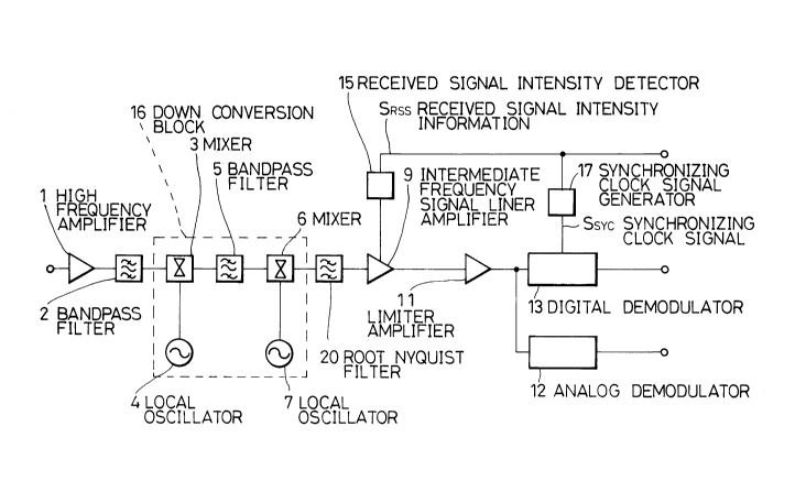
Fig. 2 shows in block form a receiver circuit for
receiving both digital and analog modulated signals
according to a first embodiment of the present invention.
Those parts shown in Fig. 2 which are identical to those
of the conventional receiver circuit shown in Fig. 1 are
denoted by identical reference numerals.
The receiver circuit shown in Fig. 2 comprises a high
frequency amplifier 1, a bandpass filter 2, a down
2U96~76
conversion block 16, an intermediate frequency signal
linear amplifier 9, a limiter amplifier 11, an analog
demodulator 12, a digital demodulator 13, and a received
signal intensity detector 15. The received signal
intensity detector 15 outputs received signal intensity
information SRss. The down conversion block 16 comprises
mixers 3, 6, local oscillators 4, 7, and a bandpass filter
5.
A root Nyquist bandpass filter 20 is connected to an
input terminal of the intermediate frequency signal linear
amplifier 9. The received signal intensity information
SRss from the received signal intensity detector 15 is
supplied to a synchronizing clock signal generator 17
which applies a synchronizing clock signal Ssyc to the
digital demodulator 13.
A digital modulated signal that has been received is
amplified by the high frequency amplifier 1 and then
limited to a certain received frequency band by the
bandpass filter 2. The digital modulated signal is
thereafter converted into an intermediate frequency signal
by the down conversion block 16. The digital modulated
intermediate frequency signal from the down conversion
block 16 is limited to a frequency band by the root
Nyquist bandpass filter 20 with root Nyquist
characteristics. Since it is impossible for the root
Nyquist bandpass filter 20 to have complete root Nyquist
- 8 - 2096~76
characteristics, the root Nyquist bandpass filter 20 has
characteristics approximate to root Nyquist
characteristics having an attenuation rate of 1/~ at a
frequency which is 1/2 the symbol rate.
An output signal from the root Nyquist bandpass
filter 20 is applied to the intermediate frequency signal
linear amplifier 9, which linearly amplifies the applied
signal. The amplified signal from the intermediate fre-
quency signal linear amplifier 9 is limited to a certain
amplitude and amplified by the limiter amplifier 11. For
digital signal demodulation, the received signal intensity
information SRss from the received signal intensity
detector 15 is supplied to the synchronizing clock signal
generator 17. The synchronizing clock signal Ssyc from
the synchronizing clock signal generator 17 and the output
signal from the limiter amplifier 11 are applied to the
digital demodulator 13, which produces a digital
demodulated signal.
An analog modulated signal that has been received is
processed into an intermediate frequency signal by the
same circuit components as the digital modulated signal up
to the limiter amplifier 11. The output signal from the
limiter amplifier 11 is applied to the analog modulator
12, which produces an analog demodulated signal.
Fig. 3 shows in block form a receiver circuit for
receiving both digital and analog modulated signals
- 9 - 2096~76
according to a second embodiment of the present invention.
The receiver circuit shown in Fig. 3 differs from the
receiver circuit shown in Fig. 2 in that the output signal
from the limiter amplifier 11 is applied to a
synchronizing clock signal.generator 18 which generates a
synchronizing clock signal Ssyc and supplies it to the
digital demodulator 13.
A digital modulated signal that has been received is
converted into an intermediate frequency signal which is
passed through the root Nyquist bandpass filter 20 and
then amplified by the intermediate frequency signal linear
amplifier 9, as with the first embodiment. The amplified
signal from the intermediate frequency signal linear
amplifier 9 is limited to a certain amplitude and
amplified by the limiter amplifier 11. The amplified
signal from the limiter amplifier 11 is supplied to the
synchronizing clock signal generator 18, the digital
demodulator 13, and the analog demodulator 12. The
digital demodulator 13 demodulates the signal from the
limiter amplifier 11 into a digital demodulated signal
with the synchronizing clock signal Ssyc from the
synchronizing clock signal generator 18. The analog
demodulator 12 demodulates the signal from the limiter
amplifier 11 into an analog demodulated signal.
Although certain preferred embodiments of the present
invention have been shown and described in detail, it
lO- 2096476
should be understood that various changes and
modifications may be made therein without departing from
the scope of the appended claims.