Note: Descriptions are shown in the official language in which they were submitted.
~0~6~~5J
_ 1 _
RESONANT POWER FACTOR CONVERTER
FTELD OF THE INVENTION
This invention relates to improvements in
devices for increasing the power factor in power circuits
supplying DC power to a DC load having a complex impedance.
More particularly, the invention is directed to a novel
converter for interpositioning between an AC source and a
DC load which will essentially maintain a unity power
factor (UPF) independent of the load impedance.
BA T~ ~,OUND OE' THE INVENTION
In AC circuits, power factor is defined as the.
ratio between the real power measured in watts and the
apparent power which is the product of the rms voltage and
the rms current. The ideal situation is where the power
factor is 1, namely that all of the apparent power is real.
This occurs when the current drawn from Hydro "looks" like
the Hydro voltage, i.e., perfectly sinuosity and in phase
with the voltage so that in looking at the two waveforms,
it would not be obvious which was which the voltage or the
current. With unity power factor the power taken is
20~~~~~
- 2 -
P = V * I cos (~> * D.F.
where V = line voltage
I = line current in amperes
B = phase angle between V and I
D.F. = Distortion Factor
Total Power /Power o.f Fundamentals
Since B the phase angle is 0, cos 0° is 1 and D.F. is 1 and
P = V * I watts.
If the power factor is less than one, then some
or all of the apparent power is not real power and thus is
being wasted. In AC circuits the voltage and current are
sinusoidal and in phase when the load is a pure resistance
or when the impedance of the load is such that the
inductance and capacitance of the load balance out and the
load is seen as a resistive load. If the impedance of the
load is a simple inductive load, the current will still be
sinusoidal but will lag the voltage. On the other hand, if
the load is a simple capacitive load it will still be
sinusoidal but will lead the voltage. In both cases the .
power factor. will be less than unity because Cos 8 will be
less than 1 and would equal 0 for a theoretical circuit of
pure inductance or pure capacitance where the phase
difference between the voltage and current is equal t o 90°.
- 3 -
For many years, linear loads were the largest
portion of the AC distribution system, the bulk of which
were resistive loads from lighting and heating elements and
inductive loads from motors. As inductive loads caused the
current waveform to lag the voltage waveform, to balance
the system it was only necessary to add capacitance to the
line. However, this is no longer sufficient.
In recent years, there has been an increase in
the number of off-line switching non-linear DC power supply
loads on the AC distribution systems of electrical
utilities. The proliferation of these nan-linear loads has
caused problems for the electrical distribution utility
systems due to 'the presence of harmonic distortion as
measured by the distortion factor.
The blocking effect of the input diodes and the
presence of filter capacitors in such off-line power
supplies employing diode rectifiers and filter capacitors
causes distortion of the current waveform from a sinusoidal
to a complex waveform of tall peaks made up of the
fundamental frequency (typically 60 Hz) and a number of
harmonics or multiples of the fundamental frequency summed
together. As it is only the fundamental waveform 'that
contributes to real power, the presence of harmonics can be
detrimental for the utility in many ways. Firstly,
utilities only charge for real power used and the harmonics
DSJ-8638
_ q
do not contribute to real power. Additionally utilities
utilize a common neutral wire in 'their distribution
systems. For linear loads, the return current flows in the
neutral wire were algebraically cancelled, resulting in no
current flow in the neutral wire. The harmonics generated
by non-linear loads cannot be cancelled in the usual manner
and in fact are additive which can produce dangerous
overloads and heating of the neutral wire and central
distribution transformers.
Uncorrected off-line switching power supplies
generally have a power factor. of about 0.65. This means
that total currents of 1.59 (1/0.65) times those of t he
fundamental current are required 'to produce the real power
and that uncorrected power supplies can only draw 65% of
the power of a corrected power supply from the same input
current. These high peak currents can trip over-current
devices, can cause distortions in the voltage waveforms and
can cause clipping of both voltage and current waveforms.
Because of these problems, substantial interest
in power factor correction for DC power supplies has
emerged. This has led in part to the establishment of
standards such as European Community Standard IEC-555-2
IEEE 519, and MIZ 1399 which regulate the amount of
permissible disturbances caused by appliances and other
equipment connected to AC lines.
DSJ-8638
2D~~~~~
- 5 -
There have been many proposed methods of power
factor correction for DC power supplies including passive
filtering, multiphase rectification, ro1:ary reactive
correction, shunt electronic correction, series electronic
correction and combinations of the above. However, all of
these techniques present certain drawbacks. For example,
passive filters, which involve filtering of the known
frequencies of the harmonics, tend to be large, heavy and
expensive and can introduce phase shifts further degrading
power factor.
At the present time, most commercial systems for
power factor converter use high frequency active
waveshaping techniques to achieve performance on a wide
range of operating conditions. Many of 'the schemes use a
boosting feature of pulsewidth modulation (PWM) boost class
converters, hard switched converters or their resonant-
switch counterparts. The series resonance converter has
some desirable power factor characteristics. However, due
to its voltage step down characteristics, it cannot
maintain'line current into the valleys of the input AC wave
and must be shut off typically when the line voltage falls
below 500 of its peak value.
2096 ~~~
- 6 -
described in IEEE TRANSACTIONS ON INDUSTRY APPLICATIONS,
VOL IA-19, pages 586-599, July/August 1983, by Kocher and
Steigerwald. The converter was a well-known flyback
converter utilizing a field-effect transistor (FET)
operating at 45 kHz as a high frequency switch. The
shaping of the input current waveform was obtained by
modifying the converter to pulsewidth modulate the input
power. The control system adjusted the magnitude of the
sinusoidal input current to achieve variations in DC output
power level. However, the converter described, while
achieving a high power factor under high power
applications, only exhibited efficiencies o.f the order of
60 to 70~ under low power applications. w
A series/parallel LCC resonant circuit in a high
voltage boost, wide bandwidth configuration has been
described in an overly simplified schematic manner in IEEE
1991, pages 5 to 16 by Schutten et al. The reference
describes the simulated performance of a parallel resonant
converter and a combination series parallel resonant
converter when operated at a fixed frequency achieving a
respectable power factor but far from regulatory
requirements. However, active control of a series parallel
converter is required to maintain zero voltage switching
conditions above resonance under all conditions. Switching
above and below the resonant frequency based upon the input
line current would cause stress on, and probably
DSJ-8638
2fl~~~~~
destruction of, the system component. The reference does
not disclose any means for the active control of this
system and as far as 2 am aware no satisfactory control
means has ever been proposed.
~iIMMARY OF THE INVENTION
The present invention is directed to a novel
converter for interposition between an AC power source and
a DC load capable of maintaining a substantially unity
power factor independent of the impedance of the load.
According to the invention, the converter has rectifying
circuit means to provide DC power to a DC power output .
circuit from an AC source, means for varying the impedance
seen by the AC source in the DC output circuit, and means
responsive to a shift in AC input current away from an in-
phase relation with the voltage of the AC source under
loading of the DC power output circuit for controlling said
impedance varying means in a direction to return the AC
current towards in-phase relation with the AC voltage.
More particularly, according to the preferred
form of the invention, the means for varying the impedance
20~6~~~
therefor responsive to 'the DC voltage of the DC output
circuit and the phase between the AC voltage and AC '
current, said control converter including a variable
impedance responsive to 'the resonant circuit current for
controlling the phase angle between the resonant circuit
current and voltage across the resonant circuit.
BRIEF DESCRIP~IbN OF SHE DRAWINGS
The above as well as other advantages and
features of the present invention will be described in
greater detail according to a preferred embodiment of the
present invention in which: '
Figure 1 is a block diagram of a converter
embodying the invention;
Figures 2A to 2F constitute a simplified
schematic diagram of the system of Figure 1 with:
Figure 2A showing the input diode component,
Figure 2B showing the FET bridge and resonant
circuit,
Figure 2C showing the isolation transformer,
output diode and output capacitor, and
Figures 2D, 2E and 2F showing the UPF control
circuit;
Figure 3A is a diagram of the sinusoidal hydro
~09'~65~~
- 9 -
Figure 3B is a diagram of the current for unity
power factor;
Figure 3C is a diagram of the typical current of
a low power factor converter which is full of harmonics;
Figure 4A is a diagram of the hydro voltage;
Figure 4B is a diagram of the voltage after the
diode bridge of Figure 2A when the capacitance across the
bridge is small;
Figure 4C is a diagram illustrating what the
voltage after the diode bridge of Figure 2A would be if the
capacitance across the bridge was large;
Figure 5A is a diagram of the voltage waveforms
from the full FET bridge of Figure 2B;
Figure 5B is a diagram of the resonant current
flowing from the FET bridge into the resonant circuit of
Figure 2B through L1 and CT1-prim;
Figure 6 is a diagram illustrating the gain of
the series/parallel converter as a function of frequency
and output loading (Q) with the horizontal line marking the
controlled output voltage desired:
Figures 7A and 7B are diagrams of the inverter
FET and resonant circuit voltage and current waveforms
respectively at light load;
Figure 8 is a diagram depicting the basic phase
control circuit;
Figures 9A to (c are diagrams illustrating the
basic waveforms of the phase control circuit with:
DSJ-8638
2~96~~~
- 10 -
Figure 9A .representing the drive current,
Figure 9B representing the drive voltage, and
Figure 9C representing the comparator output
voltage constituting the FET drive;
Figure l0A is a diagram of the FET drive current
waveforms;
Figure 10B is a diagram of the FET drive voltage
waveforms;
Figure 11 is a simple schematic diagram of the
FET drive amplifier;
Figure 12A is a diagram of the FET drive
waveform without shaping; and
Figure 12B is a diagram similar to E'igure 12A
but showing the effect of a resistor diode shaping network.
DETAINED DESCRIPTION OF THE PREFERRED EMBQDIMENTS
The present invention provides for a novel
technique and circuitry that produces essentially Unity
Power Factor (UPF) as seen from the AC hydro source. A
particular advantage of the invention is that it is not
limited in either the DC power output it can provide or the
AC power sources to which it can connect as have other
Power Factor improving devices. Other important features
of the invention are the cost, size and weight advantages
at higher power levels over other known Power Factor
improving devices.
DSJ-8638
2~~6~5~
- 11 -
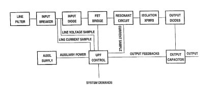
Figure 1 shows a block diagram of a converter
embodying the invention. The input power is conditioned
through a line filter for EMI/RFI (Electromagnetic
Interference and Radiofrequency Interference) located as
close to the AC terminals as possible. The voltage is then
applied to an input diode stage, preferably a diode bridge
to farm the DC rail voltage in a typical manner. However,
this DC rail has minimal energy storage and the voltage on
the DC rail follows the envelope of the input AC voltage.
The output from the input diode stage is applied
to an inverter stage comprising a FET (Field Effect
Transistor) bridge stage, preferably, a full FET bridge
which chops the DC rail voltage and applies it to the
resonant circuit stage which is loaded by an isolation
transformer, preferably an hCC or a series/parallel
resonant circuit configuration. An innovative phase
control technique, described below is used to control the
inverter stage.
~U96~~~
- 12 -
As hereinafter more fully explained, the control
of the inverter to give the desired UPF is effected by
sensing the output DC voltage, the AC input voltage, the AC
input current and applying any change in the sensed DC
output voltage or any phase difference between the sensed
AC voltage and AC current to a control circuit responsive
to the current flowing in the inverter circuit to control
the gating of the FET bridge to restore the system to its
desired operating condition giving rise to UPF.
Figures 2A to 2F illustrate a simplified
schematic diagram o.f the UPF converter shown in block
diagram in Figure 1. It consists of the full input diode
bridge D1 in Figure 2A which creates a DC rail or buss
voltage although it will be understood other rectifying
circuits may be used if desired. The DC rail or buss has
minimal energy storage on it, essentially only enough
capacitance to supply a low impedance (at elevated
frequencies) to the resonant current flowing in the
resonant circuit. Additional low energy filtering may be
used to reduce the filtering requirements of the line
filter.
Operating off the DC rail is a full'bridge of
FETs Q1, Q2, Q3 and Q4 shown in Figure 2~ in an above
resonance, zero voltage switching scheme, complete with a
DSJ-8638
~a~~5~~
- 13 -
lossless snubber controlling the rate of use of voltage
across the FET elements. While 'the full FET bridge is
preferable, a half bridge circuit could also be employed.
This full bridge is shown in Figure 2B as running a
series/parallel LCC resonant circuit L1, C6, C7 and current
transformer primary CT1-prim in a high voltage boost, wide
bandwidth configuration although a parallel resonant
circuit could be used.
The output of the resonant circuit is loaded by
the output transformer T1 in Figure 2C which both isolates
the output voltage as well as allowing any desired output
voltage, in this case 62 Vdc. The transformer reflects the
load of the output diodes D6 and capacitor C8 onto the
resonant circuit. The output capacitor C8 is loaded by the
DC output of tr~e converter, or its equivalent resistance.
The control system for the inverter Figure 2D
senses the DC output voltage and compares it against a'
reference voltage in a standard error amplifier circuit U1
which regulates the output voltage. The error signal is
multiplied by a representation of the sinusoidal input
voltage in a four quadrant TC multiplier I~C1995L to create
a reference signal whose magnitude keeps the output at the
right voltage, but the waveshape, both in magnitude and
phase, is the waveshape that the 3.nput line current must
have t o realize Unity Power Factor and thus constitutes a
DSJ-8038
~09~~~9
- 14 -
reference line current waveshape. An input current error
amplifier L~2 compares the phase of the reference line
current against the actual line current and when there is a
difference, the input error amplifier creates an error
signal to a resonant inverter control circuit Figure 2E to
control the instantaneous power output of the inverter so
that its input power pulls a line current whose
instantaneous magnitude at all times matches the reference
current signal. This error signal is reflected as a DC
current in a current source transistor Q5 which controls
the DC current in a variable impedance in 'the form
illustrated within the doted lines in Figure 2E as a
variable inductor. This inductor is connected in a
resonant tank circuit C12, R19 responsive to the current in
the inverter resonant circuit through transformer CT1-
secondary which resonant tank circuit controls the FET
bridge operation as hereinafter more fully described.
Such a circuit arrangement provides a novel
phase control system for the inverter circuit by
controlling the phase angle between the resonant current
waveform and the switched DC rail voltage.
Power output of the inverter bridge at any time
is given by the relationship.
P = V * I cos (0)
DSJ-8638
- 15 -
where V = effective AC rail voltage (.9 * V DC)
I = resonant current (rms fundamental)
0 = phase angle between V and I
A truly novel characteristic of this converter
in that it allows the volt-amperes of the primary circuits
to closely match the output power at full load. In an
actual embodiment constructed in accordance with the
circuit of Figure 2, 4.,0 KVA was utilized in the primary
circuits to realize 3.4 Kw output power at near full load.
To control the phase angle, a novel technique is
employed utilizing a variable impedance shown within the
dotted lines in Figure 2E as a variable inductor comprising
two small current transformers having a primary to
secondary ratio of 50 to 1, usually referred to in the art
as a linear variable inductor. The linear variable
~0~~~~~
- 16 -
impedance and hence the phase angle of the voltage across
the tank circuit may be varied. A simple comparat or U3 in
Figure 2F watches the zero crossings of the voltage
generated in the tank circuit in response to the resonant
current to. produce the gate drive timing waveforms, which
are then amplified to become the actual gate drive which
runs the FET gates through a pulse transformer. The
comparator U3 output waveform is used to produce the gate
drive waveform.
The gate drive shown in Figure 2F is a very
simple one. Other gate drive schemes that turn the FETs
off quicker may be used in certain applications if desired
as will be apparent to those skilled in the art. There are
currently many standard circuits available to control FET
drive turn-off which would be suitable.
A parallel resonant tank has a possible
impedance swing of 180 degrees from +90 degrees to -90
degrees. However, as the complex impedance angle is a
"tangent" term, the extremes of +90, and -90 degrees are
never reached. Effectively, the control range, from
experience, is approximately 135°. To control the output
power, however, only a 90° swing is required. Care must be
taken that the inverter never runs at a frequency below the
resonant frequency of the LCC circuit.
DSJ-8638
20~6~~~
- 17 -
The operation of the UPF converter illustrated
in Figures 2A to 2F will now be described in further
detail. The converter is powered from the utility which
connects to the UPF circuits at the AC input AC1.
Connection of the utility here applies voltage at a nominal
frequency of 60 Hz. Figure 3A illustrates this voltage
waveform. The AC input voltage is measured by the primary
side of transformer T2 (T2-prim). The secondary of
transformer T2 (T2-sec) creates a voltage that "looks'°
identical to the AC input voltage, but it is now smaller in
magnitude, and no longer directly connected to the utility.
This voltage is used to measure the AC input voltage
waveform so that the control circuits have a model of the
AC input voltage waveform to follow. This voltage is
exactly representative of the AC input voltage arid can be
found at TP1 in Figure 2.
The AC input flows through the primary of
current transformer CT2 (CT2-prim). The AC input current
flows through this current transformer primary, and an
exact representation of this current flows in the secondary
of the current transformer CT2 (CT2-sec). If the load is
pure resistance, i.e. unitary power factor, the waveform
would be as shown in Figure 3B. This secondary current,
which is exactly representative of the AC input current,
flows into the resistor R10 in Figure 2D, creating a
voltage across resistor R10 which is exactly representative
DSJ-8638
209~~5~
- 18 -
of the AC input current. that is flowing. This voltage can
be found at TP2 of Figure 2D.
At this point we have small signal
representations of the AC input voltage and current that
the UPF regulator is drawing from the utility.
The AC input voltage flows through a "Full
Bridge" of diodes D1 in Figure 2A. This full bridge of
diodes D1 makes the voltage on the other side of the full
bridge always positive, thus the AC voltage supplied by
Hydra has been turned into a DC voltage. Figure 4A
illustrates the voltage waveform, called a "DC buss" after
the full bridge of diodes. The capacitors connected across
the DC buss are very small, hence they have no or little
effect on the voltage waveform, and the voltage waveform is
indeed as illustrated in Figure 4B.
This DC buss voltage waveform from the output of
the diode bridge has a full bridge arrangement of FETs Q1,
Q2, Q3 and Q4 connected across it. The FETs are 'turned on
diagonally, first the upper left Q1 and the lower right Q4
FETs are 'turned on, then these are turned off and the lower
left Q2 and upper right Q3 FETs are turned on. This
diagonal on and off action of the FETs applies the DC buss
voltage to the resonant circuit L1, C6, C7, and CT1-prim
first one way, then the other way, effectively placing a
- 19 -
square wave alternating (see Figure 5A) voltage of first
+DC buss, then -DC buss driving the resonant circuit. This
alternating voltage action can be applied at any frequency.
Applying a square wave voltage onto the resonant circuit
makes current flow in the resonant circuit Figure 5B. The
specific shape of the resonant current i.s a function of the
frequency at which the square wave is applied, the values
of the resonant components and the loading or Q on the
resonant circuit.
It is the variation of the .frequency of the
square wave DC buss valtage that is used to control the
power. As the frequency is increased, the power drawn from
the DC buss is reduced. In the illustrated circuit of an
actual example, a frequency variation of approximately 125
kHz to approximately 175 kHz results in a power range of
full power to no power.
At this point we have a square wave +/-DC buss
voltage applied to the resonant circuit at a frequency
which we determine. As the frequency is varied, the power
drawn by the full bridge is varied, thus the power drawn
from Hydro is varied.
The excitation of the full bridge of the FETs
will make a sinusoidal current flow in the resonant
circuit. This cu Trent flows in the series branch L1 and
DSJ-8638
~QJ~~:~~
- 20 -
C6, then in the parallel branches C7 and the primary of T1
Figure 2C. The current then returns through the primary of
the current transformer CT1-prim.
During the positive half cycle of the sinusoidal
resonant current, the current in C7 will cause the voltage
on C7 to rise. This voltage on C7 is reflected by the
transformer T1 to the secondary diodes D6 in Figure 2C
which are blocking the output voltage. At some time, the
voltage on C7, hence the secondary voltage, will rise to a
point where the diodes D6 becomes forward biased, and start
conducting. At this point, the primary resonant current
will flow through the transformer T1, through the output
diodes D6 conducting and into the output capacitor C8 in
Figure 2C. This current flow at the output voltage is the
output power.
The output capacitor C8 is so large it can
absorb and give out the resonant and load current during
the switching cycle, without any substantial change in
voltage on it, Thus this forms the DC output voltage of
the converter. The user places a load on this capacitor,
current flows, and this current at this voltage forms the
output power. The function of the cone rol circuits are to
,act to control the power flow such that the output power
into the large output capacitor equals the load power taken
away from the output capacitor.
DSJ-8638
- 21 -
Figure 6 illustrates the magnitude of the output
voltage as the frequency and load resistance is changed.
The horizontal scale shows the change as frequency is
increased and the vertical scale shows the output voltage.
The various Q's listed show 'the effect of changing the load
resistance on the converter. As the load resistance is
decreased, Q increases. A single horizontal line, VD in
Figure 6 represents a desired output voltage of operation.
Clearly, as the load parameters (Q) change, the frequency
must change in order for the same output voltage VD to
occur, i.e., the same output voltage must intersect the
different Q lines only at different frequencies.
For the purposes of this circuit, only operation
above resonance is considered. This is the area of the
falling magnitude of the output voltage as frequency is
increased, essentially to the right hand side of the
figure.
Figures 5A and 5B illustrate what the voltage
and current waveforms actually look like. The voltage
waveform leads the current waveform thus indicating that
that the circuit is operating above resonance. If the
voltage lags the current, the circuit would be operating on
the wrong side of the resonance and 'tremendous stress on
the switching devices (and probable destruction) would
DS,~-8638
20~~~~~~
- 22 -
occur. One feature of the control strategy implemented is
it prevents this from occurring.
Figures 7A and 7B also illustrate respectively
the voltage and current at light load. Here, the voltage
leads the current by a substantial amount. This is at a
somewhat higher frequency of operation, or to the far right
of Figure 6. If we compare this to the high power
condition (Figures 5A and 5B), it can be seen that at low
power, the current lags the voltage by a phase angle of
almost 90° while at high power, the phase angle is
substantially less, about 18°.
Thus, at high power, which is a lower frequency,
there is an 18° phase difference between the voltage and
current. At low power, the frequency is higher and there
is a substantial phase difference of 90°. This relates
quite well with the basic power formulae:
P = V * T cos (B)
where P = power
V = voltage
I = current
~ = phase angle between V and I
At low power, the frequency is high, the angle
(9) is 90°, cos (8) - 0, V I cos (B) is 0, and thus the
DSJ-8638
20J~j~~
- 23 -
power is 0. Zero power drawn by 'the FE~P bridge will draw
zero current from Hydro.
At high power, the frequency is lower, the angle
between the voltage and the current (6) is small, cos (0)
is approximately 1, and power (V I cos (0)) is V I,
essentially the actual power required from Hydro to handle
the load supplied to the DC output circuit and hence the DC
load. This power must be current drawn from Hydro.
Thus by controlling the frequency of the
inverter circuit, the phase angle B can be controlled,
hence the output power of the inverter and 'the current
drawn from Iiydro can be controlled.
,
However, Figure 6 shows also that as the load on
the converter or Q is changed, the resonant frequency is ,
changing. Thus, using only control of frequency to control
the system may have a substantial chance of being on the
wrong side of resonance as the load resistance hence Q is
changed since the resonant frequency has changed.
Operation on the wrong side of resonance, i.e. below
resonance, is disastrous to the power circuits.
An increase in frequency results in less power
and an increase in the angle (B) between the voltage and
the current. Thus, if the angle (B) is controlled, the
DSJ-8638
~Q~~~~~~
- 24 -
proper frequency would result and the pawer would be
controlled as a result of the cos (B) term of the basic
power formulae. Control of the angle (f~) controls the
frequency and the converter power directly without having
to wait for the inertia of the resonant circuit to change
its current in response to a change in frequency. This
leads to improved controllability of the converter. As
we7.l, since the angle is controlled irrespective of the
frequency of operation changes in resonant frequency as the
load resistance, hence Q, is changed, the system will
always remain on the right side of resonance, i.e. above
resonance, essentially automatically tracking the change in
resonant frequency.
Figure 8 illustrates a simple schematic of 'this
phase control circuit which is in essence a parallel tank
circuit made up of a linear variable inductor VL, the
parallel capacitor and the resistor.
The linear variable inductor VL consists of two
current transformers connect ed beak to back. The actual
inductance is the inductance of the current transformer.
By controlling the DC current in the control winding the
inductance can be varied and cantrolled and in turn its
resonant frequency, and its complex impedance, complete
with magnitude and phase angle can be controlled. Thus, by
controlling the inductance of the linear variable inductor,
DSJ-8638
~0~~~~~
- 25 -
the phase angle across the parallel resonant circuit is
being controlled. A novel characteristic of this circuit
is that from the control winding point of view, the
voltages reflected to the control winding cancel each other
out. This means any noise or strange signal that may be
present on the inductor on one side, will cancel out on 'the
control side, leaving the control side free of this signal.
The resonant circuit of the inverter or power
circuit L1, C6, C7 of Figure 2B contains a current
transformer CT1-prim. This current transformer C'P1-prim
measures the current in the power circuit and a scaled
version of the resonant current that flows in the power
resonant circuit flows in the secondary of the current
transformer CT1-sec in Figure 2E. This current from the
current transformer CT1 now flows through the phase control
circuit. This current illustrated in Figure 9A that is
flowing in the parallel tank circuit will create a voltage,
illustrated in Figure 9B that is directly related to the
impedance, and is a function of both in magnitude and
phase. Hence, a voltage is created across the control
circuit that is directly related to the main power resonant
current and whose phase is controllable.
Referring to Figures 9A, 9B and 9C, this phase
difference can be determined by looking at where the
respective waveforms crass zero, as 'this is how the phase
DSJ-8638
2OJ~~~J
- 26 -
difference is defined. A simple comparator U3 in Figure 2F
can be used to measure where the zero crosses of the
voltage waveform occur. The output of the comparator is at
one state, or high, when the voltage is positive and at
another state, low, when the voltage is negative as shown
in Figure 9C.
For the FET gates, Figure 11 is a diagram of the
gate drive amplifier UC1709. The output of the comparator
is, in essence, the required FET gate drive signal. '.Phe
comparator chosen, an LM361, has two outputs, one output
the inverse of the other, thus the timing for the gate
drive for all corners of the full bridge of FETs is
available as illustrated in Figure 10B.
This signal, applied to a pulse 'transformer
shown in Figure 2F 'that is connected to the gates, results
in the gate waveforms shown in Figure 12A. The FET gate is
positive when the FET is on, and negative when the FET is
off. This negative gate voltage is beneficial to the FET
as it increases the error margin of the FET so that the FET
~OJG~~~
- 27 -
This avoids any problems with what is called
"shoot through", where, in some gate drives, it is possible
to have the two FETs in a leg of the full bridge on
together briefly, forming a temporary short circuit across
the DC buss, usually resulting in the destruction of the
FETs.
On the actual gate drive of the FETs, a small
resistor and diode R1, D2, etc., pefform some simple signal
conditioning. With this arrangement, the FET will turn off
quickly and turn on slowly. When the transition occurs in
the FET gate drive, the FET that was on turns off very
quickly, but the FET that will turn on next is slightly
delayed. This means there is a finite time when neither
FET is on. This helps guarantee that the two FETs are
never on together.
When the system is in control, the voltage on
the two input pins of an op-amp will always be identical.
The op°amp will always move its output voltage in an
attempt to keep the voltage on its input pins identical.
The voltage on the input pins will only be different if the
op-amp or the system is out of control. For the purposes
of this following description, the op-amps are always in
control.
DSJ-8638
209G~~~
- 28 -
Referring to figure 2D, the voltage error op-amp
U1 compares the output voltage of t he system (TP9) against
the reference voltage of the system (TP3). The system is
in control, so the voltage divider made by R7 and R18
produces zero volts (they are opposite polarity) on the
input of the voltage error op-amp U1 pin 2. This equals
the zero volts on the other pin of the op-amp. The op-amp
is in control. The feedback elements R8 and C11 are used
to stabilize the control systems.
The output of the voltage error amp (TP5) is a
specific DC voltage that, when combined with the rest of
the system, has it i.n control. The voltage TP5 is then
multiplied by multiplier MC1995T~ by the voltage on TP1
which is a representation of the AC input voltage resulting
in the same sinusoidal voltage, but a different magnitude.
As the voltage on the voltage error op-amp goes up and down
in magnitude, the output of the multiplier (TP6) will be
the same sinusoidal voltage, but it will also go up and
down in magnitude in response to the voltage error
amplifier which, when it has control., keeps the output
voltage and the reference voltage always identical.
The output of the multiplier (TP6) is the line
current reference. This waveform is identically what it is
desired that the AC input current look like. This voltage
is sinusoidal, arid "looks" exactly like the AC input
DSJ-8638
2~9~~~~
- 29 -
voltage. Its magnitude, when the system is in control, is
identically the AC input current required to create the
input power that is then transferred to the output of the
unit.
The line current error op-amp U2 compares on a
continuous basis what the desired voltage of the line
current is required to be (TP6), and what it actually is
(TP2). When in control, the op-amp U2 will keep these
voltages the same at all times. At any specific time, the
voltage divider R11 and R12 creates a voltage at the input
of the op-amp on pin 2 of U2 which is zero. This equals
the voltage on the other pin. R13 and C12 are used to
stabilize the system. When in control, the op-amp U2 will
act to maintain the voltages on its inputs identical.
The output of the line current error op-amp
(TP7) is connected to R14. R14, Figure 2D, and R16, and
Q5, Figure 2E form a circuit called a current source. In
its simplest form the current in the base resistor R14 is
- 30 -
The current in Q5 is the control current for the
linear variable inductor in the phase control circuit
Figure 2E described earlier. Resist o1 R17 provides a shunt
path for the inductor VL to guarantee that the current in
the inductor always has someplace to go. Thus, by
controlling the phase of the inverter that acts in response
to the line current error op-amp U2 whose function is to
keep the AC input current identical to the line reference
current, the AC input current is controlled.
As the voltage of the line current reference
increases due to its sinusoidal shape, it will try 'to move
the negative pin of the control op-amp U2 negative. Moving
.y the negative op-amp pin negative, the output voltage of the
a 15 op-amp U2 will move positive. As the op-amp voltage moves
.. .;
positive, there is less voltage across the current source
R14, R16 and Q5, and the current to Q5 base reduces. A
corresponding decrease in the collector current of Q5 will
occur, hence the current in the linear variable inductor VL
5
:,
"~i 20 decreases .
This will increase the inductance of the linear
~rariable inductor. As the inductance increases, the phase
angle of the inverter decreases, the cos (theta) 'term in
. w
25 the power formulae increases, the inverter draws more
power, hence the AC input current increases exactly to
match the line current reference. As the line current
DSJ-8638
:'t
20~~~~~
- 31 -
reference goes over the cycle of 60 Hz, the AC input
current drawn follows this reference.
As a result, the AC input line current "looks"
exactly like the input line voltage. This is Unity Power
Factor.
The system will now be described when the load
changes for some reason: it increases. Since the power
flow for the instant is fixed, as the load is increased,
the voltage on the output capacitor C8, Figure 2C,
decreases, as the difference in power must come Pram the
capacitor. As the output voltage decreases TP4, E'igure 2D,
the voltage on pi.n 2 of the voltage error op-amp U1
decreases. As soon as the voltage decreases, the output
TP5 of the op-amp U1 moves more positive t o keep the
voltage on its two input pins the same. This higher
voltage is then fed to the multiplier MC1495L where it is
multiplied by a scaled representation of the input voltage,
creating a larger sinusoidal line current reference voltage
TP 6 .
20~~~~~
- 32 -
current in the current source and less current will flow in
the control inductor VL of the phase control circuit in
Figure 2E. The inductance will increase,the phase
difference in the inverter will become less, and the power
matches the increased load that was added to the system.
Since the line current reference from the multiplier is.an
exact scaled replica of the AC input voltage, the AC input
current drawn by the inverter "looks" like the input
voltage, hence, the Unity Power Factor is maintained.
In reality, there are delays in the system and
circuits, hence, even though the circuits act as described,
the Unity Power Factor is not absolutely perfect at
matching the line voltage and current at all times.
However, a power fact or has been measured at .99 in
prototype development testing and the result is excellent.
The inverter control scheme is free of timing
ICs and consists only of passive devices and linear
devices. This is especially beneficial in a static or
noisy environment.
A major advantage of the present invention is
High Power Capability, the Unity Power Factor technique is
easily extended to very high pocaer - low cost 20 Kw modules
are not unreasonable. There is no reasonable mains voltage
limitation as components are currently available to operate
DSJ-8638
2Q~~~59
- 33 -
the technique at high power on AC inputs as high as 480
Vac. The present invention results in high power density
for a small size, the high frequency operation of 125 'to
150 Khz makes for small, light weight reactive and power
handling devices. The present invention achieves low cost
as the cost of the power components are reasonably low; the
implementation is quite cost effective on a per watt basis
at higher power levels. Indeed, the high power factor as
seen from the switching devices maximizes the cost
effectiveness of the approach. The technique, being
resonantly based, exhibits minimal~EMI/RFI compared to its
PwM counterparts. The present invention provides H~.gh
Power Factor over the full range of operation. Excellent
power factor with extremely low harmonic content is
maintained over all line and load conditions. The present
invention provides efficiency up to 90% and greater.
Excellent efficiency aver all conditions is maintained.
The present invention also provides inherent current
limiting on overload. Under overload conditions, current
limiting is inherent and shows up first as an increase in
the harmonic content of the input current, then as loss of
regulation of the output.
A 51 volt Unity Power Factor Converter was
constructed by breadboard using the following values for
the components:
R1 6852 R2 6852 R3 68SZ
DSJ-8638
R4 6852 R20 20052 D1 MB2510
R5 - C1 4.7~f D2 MUR110
R6 lkS2 C2 2200pf 35 D3 MUR110
R7 10kS2 20 C3 2200pf D4 MUR110
R8 lOkS~ C4 200pf D5 MUR110
R9 47SZ C5 2200pf D6 9 x MUR1620CT
R10 5SZ C6 .066~.fD7 1DI4733
R11 27kS2 C7 .l2uf 40 Q1 3 x IRFP450
' R12 6kSZ 25 C8 470, Q2 3 x IRFP450
OOO~.f
R13 97kSZ C9 4.7~.f Q3 3 x IRFP450
R14 lkS2 C10 10~f Q4 3 x IRFP450
R15 - C11 10~.f Q5 MJE120
R16 100SZ C12 2200~L.f45 U1 MC34001
R17 4752 30 C13 .22~.f U2 MC34001
R18 100k C14 1000pf U3 LM361
R19 20052 C15 10~.f
Power UC1709enhanced full Z34 and
gain by bridge
of
IRF
zRF9z3o
50 Pulse sformercustom with x F41306F errite
Tran made 10
toroids
T1 18T
primary,
4T
secondary
T2 208/5VTransformer
CT1 Pulse
PE51686
50:1
55 CT2 200:1
on
steel
core
209~~5~
- 35 -
such as soft start, feedback loop rolloff, etc. as they are
not necessary for a full understanding of the invention.
Persons of ordinary skill in the art will easily understand
the standard features not specifically illustrated and will
be able to add them to the converter described. In
addition, it will be undertood by persons skilled in the
art that the values of the components are not essential
limitations but alternative equivalent components may be
substituted therefor.
Although various preferred embodiments of the
present invention have been described herein in detail, it
will be appreciated by those skilled in the art, that
variations may be made thereto without departing from the
spirit of the invention or the scope of the appended
claims.
DSJ-8638