Note: Descriptions are shown in the official language in which they were submitted.
-~-0 9 ~ 67 ~
INTERFACING DEVICE FOR A COMPUTER GAME SYSTEM
This invention relates to computer game systems and it
relates particularly to an interfacing device suitable
for modifying the manner in which a computer game is
played.
In many known computer game systems the
characteristics of a game, particularly its degree of
difficulty, are to a large extent predetermined by the
data stored in the external data storage medium, such
as a game cartridge.
Interfacing devices for detachably interconnecting the
processing unit of a computer game console to an
external data storage medium and which are capable of
operating in various ways, user-selected or preset, to
modify the rules of the game and thereby enhance the
playability of the game are known.
However, in some computer game systems, the processing
unit may execute checksum and memory checking routines
which would inhibit execution of a program in the
presence of an interfacing device.
In such cases, it is desirable that an interfacing
device such as that described should not respond to
addresses that are routed onto the main address bus
2~ fi7~
--2--
solely as a consequence o:E such self-checking
activity.
It is one object of the present invention to provide
an interfacing device having the capability to inhibit
data replacement should self-checking activity be
detected.
According to one aspect of the invention, there is
provided an interfacing device for connecting the
processing unit of a computer game system to an
external data storage medium to enable the processing
unit to address and receive data from different
storage locations in the external data storage medium,
the interfacing device comprising means for comparing
a reference address and addresses from the processing
unit, means for modifying data processed by the
processing unit in dependence on the comparison, and
control means for monitoring addresses from the
processing unit to detect for self-checking activity
and for inhibiting the modifying means if self-
checking activity is detected.
In a preferred embodiment, the control means
determines whether addresses from the processing unit
lie inside or outside an address block which is of
predetermined size and contains the reference address,
~2 ~ 7 ~
--3--
and utilises the results of the determination to
detect for self-checking activity.
In general, each address in the address blcck may
consist of N bits and the address bock consists of 2N-n
addresses, where N> n, and each address has the same
combination of N-n high value bits and a different
respective combination of n low value bits.
The determination made by the control means may be
utilised in accordance with different criteria to
detect for self-checking activity.
In one embodiment, the control means inhibits the
modifying means provided m consecutive addresses from
the processing unit are determined to lie outside the
address block, and the modifying means is released
from the inhibition of inhibiting means provided p
consecutive addresses from the processing unit are
determined to lie inside the address block and to have
values less than that of the reference address.
2~n~,~rll~
In this case, the sustained address activity outside the
address block is deemed to be an indication ~hat
self-checking is in progress.
In another embodiment of the invcntion, the control means
inhibits the modifying means provided that a succession of
R addresses from the processing unit is determined to lie
inside the address block and successive ones of the R
addresses are separated by no more than ~ addresses from
the processinq unit outside the address block, where N is
a preset integer and said succession of R addresses is the
succession of addresses lying below the reference address
or the succession o addresses lying above the reference
address.
~ccording to another aspect of the invention, there is
provided an interfacing device for connecting the
processing unit of a computer qame system to an external
data storage medium, to enable the processing unit to
address, and receive data from different storage locations
in the external data storage medium, the interfacing
device comprising means for comparing a reference address
with addresses from the processing unit, means for
comparing data from the external data storage medium with
reference data, means for modifying data processed by the
processing unit in dependence on said comparison of the
reference address and the addresses from the processin~
unit, and means for inhibiting the modifying means during
a current read access cycle of the processing unit in
response to a said comparison of data carried out
selectively during the current read access cycle or during
a read access cycle earlier than the current read access
cycle.
The means for inhibiting the mod:ifying means may comprise
a serial arrangement of latches ~or temporarily storing
the results o~ the comparisons of data carried out during
successively earlier read acces~ cycles, and means for
utilising a selected said result to inhibit the modifying
means .
Accordinq to a further aspect of the invention, there is
provided an electrical circuit or detecting or
self-checking activity on the address bus of a processor,
comprising mean6 for determining whether addresses on the
address bu~ lie inside or outside an address block
containing a predetermined reference address, and for
utilising the result of the determination6 to detect for
self-checking activity.
Embodiments of the invention will now be described, by way
of era~ple only, with reference to the accompanying
drawings, in whlch:
Figu~- 1 is a block ~chematic diagram showing a prior
art interfacing device
Fiqure 2 shows an electrical circuit ~orming part o~ an
interfacinq device according to the present invention; and
20 ~7 ~
-- 6 --
Figurs 3 illu~trat~ in detail a component of the electrical
circuit ~hown in Figure 2
In ord~r to clarify operation of the pr~nt inv~ntion a prior
art interface device will fir~t b~ de~cribed with reference to
Figure 1
Referring to Figure 1 the prior art interfacing device ha~ a
main addres~ bu~ 1 for interconnecting the addre~ bu~ 1 of the
proces~ing unit (PU) and the addre~ bu~ 1 of the external
memory (EM) enabling addre~es to pa~ from the proce~sing unit
(PU) to the external memory (EM)
Similarly a main data bu~ 2 interconnects the data bus 2 of the
proce~ing unit (PU) and the data bus 2 of the external memory
(EM) enabling data to pass from the external memory (EM) to the
processing unit (pu) in response to addresse~ received over the
addres~ bu~ 1
Tho interfacing de~ice haa an addr-~s latch 3 and a data
latch 4 whiCh stor- a reference adaresa A~f and
replacement data Drep respectiv-ly ~he stored
refer-nc- addr-ss Ar~f it rout-d tO a ~irst input Itl)
o an addreaa comparison cireuit 5 via a subsidia~y
address bus 6 and the stored replacement data D~p is
routcd tO ~n input of a data switching circuit 7 via a
subsidiary data bus 8
AS Figuro 1 show~, addres~eJ on the main addre5s bus
(whiCh are generated in the proC-Ssing unit (PU) of the
computer ga~ S console) are routed tO a aecond input I(2)
of the ~ddress comparison cirCuit 5 wherein they are
compar-d with th- reference addresa ~r~f recei~ed at
input I(l)
2 ~ 7 ~
-- 7 --
If the compared addresses are different, data stored
in the addressed storage location of the external
memory (EM) is routed via the data switching circuit
7 onto the main data bus 2 for onward transmission to
the processing unit.
Conversely, if the compared addresses are the same,
the address comparison circuit 5 outputs an actuation
pulse onto line L causing the data switching device 7
to change its switching state, in order to block
transmission of the data from the external memory and
route the replacement data Drep onto the main data bus
2 for onward transmission to the processing unit (PU).
By this means, the replacement data Drep is substituted
for the data stored in the addressed storage location
of the external memory, upon recognition of the
reference address Aref.
The reference address Aref and the replacement data Drep
need not necessarily be prestored in latches 3 and 4.
Alternatively, the reference address and replacement
data could be selected by the user.
The present invention will now be described with
reference to Figures 2 and 3.
rn the described embodiment, the reference address Are~
com~rises a 23 bit word, consisting o eight low value
bits ~l-a) and fifteen high value bits t9-23)-
The reerence address A~e~ occu~ies an address blockconsistinq of 256 (i.e. 23) different address words.
The address words forming the address block all have the
same combination o~ hiqh value bits (9-23), which
~combination is unique to all addresses inside the address
block, and eaeh address word has a different respective
combination of low value bits ~1-8). Accordingly, the 256
address words have consecutive values spanning the address
range of the address block.
As al~eady e~plained, addresses routcd onto the main
address bus by the ptoCessing unit of a computer game
console a~e compared with the reference address Are~.
An address received by tho interfacinq device from the
proces3ing unit will lie inside tbe address black if the
high value bits (9-23) of the compared addresse~ are the
same, and the receive~ address will lie outside the
address block if th- high value bits (9-23) of thc
compared addresses are diferent.
~f self-checking routines, such as check sum and memory
checking procedures are in progress this ~ay result in
increased activity on the main address bus of addresses
lying outside the address block containing the reference
address Aref.
2~9~7 ~
As will be e~plained, control circ:uitry, shown in Figure 2
of the drawings, determines whether each successive
address received over the main address bus 1 lies inside
or outside the address block containing the reference
addr~ss Aref, and is oPerative to utilise the resulting
determinations to evaluate the relative levels of address
activity inside and outside the address block, whereby to
determine whether or not self-checking routines arc in
progress.
If it is determined that self-checking routines are in
progreSs, the control circuitry generates a cloakin~
signal which has the effect of inhibiting the associated
data switching circuit (not shown in Figure 2) of the
interfacing device, preventing data replacement from
taking place. ~ore specifically, the cloaking signal
prevents the aforementioned actuation pulses from being
routed to the data switching circuit over line ~.
2~ i7~
The control circuitry shown in Figure 2 wil~ now be
described in more detail and, in what follows, the
convention is adopted that a true condition is hiqh and a
false c~ndition is low.
Referring to Figure 2, an address latch 20 stores the
reference address A~ef which, as already explained,
comprises a 23 bit word, consisting of eight low value
bits (l-a) and l~S high value bits (9-23).
The reference address Aref is supplied to a first input
I~l) of an address comparison circuit 2], whereas a second
input I(2) of the address comparison circuit 21 is
supplied with addresses (each consisting of a 23 bit word)
which arc routed over the main address bus 1 from the
processing unit of the computer game console to which the
interfacing device is connected.
As shown in Figure 2, the address comparison circuit 21 i.s
comprised o~ two parts; a first part 21~ which compares
the high value bit.s (~-23) of the rece~ved addresses, and
a second part 21~ which compares the low value bits (1-8)
of the received addresses.
The first part 21' of the address comparison circuit 2~
has a single output O(l) connected to respective inputs of
2~96~7~
a ~'read outsid~ block detector~ and a ~read inside block
detector in the form of inverted-input AND gate 22 and
AND gate 23 respectively. The other input terminals o
gates 22 and 2~ are connected to receive read access
pulses from the processing unit transmitted over a rcad
access line, referenced RA.
~f the first part 21~ of address comparison circuit 21
determines that the high value bits of the compared
addresses are the same (indicating that the current
address received from the processing unit lics inside the
address block) this will cause output O(l) to go high
which, in turn, causes the output of the "read inside
block detector~' ~i.e. AND gate ~) to go hiqh.
Conversely, if the first part 21' of the address
comparison circuit 21 determines that the high value bits
of the compared addresses are different (indicating that
the current address received from the processing unit lies
outs$de the address block) this will cause output O(l~ to
go low which, in turn, causes the output of the "read
outside block detector~ (AND gate 22) to go high.
The output Otl) of the first part 21~ of the address
comparison circuit 21 is also connected to the inputs of
three further AND gates 24,25,26, and each such further
AND gate ls also connected to a respective output 0(2),
- 12
209~67 1
0(3) and o(q) of the second part Zl o~ the dddress
comparison circuit 21. The olltpUt of each gate 24,25,26
is connectcd to a respective further AND gate 29,28,27,
these further AND gates 29,28,27 also being connected to
the read access line RA.
The second part 21~ of the address comparison circuit 21
compares the low value bits (1-8) of the reference address
Are~ (which has a value XXX, say) with the low value
bits oÇ the current address (which hax a value YYY, say)
transmitted over the main address bus 1, and the
respective outputs 0(2), 0(3) and 0(4) will go high if the
value YYY is determined to be greater than, equal to and
less than the value XXX.
With the described configuration of gates, the outputs of
AN~ gates 29, 28 and 27 will be high provided that the
current address transmitted over the address bus 1 lies
inside the aforementioned address block and that the low
value bits (1-8) of that address have a value (YYY) which
is respectively greater than, equal to and less than thc
value ~XXX) of the reference address Aref.
The output of AND gate 22 ~which goes high whenever the
current address is deter~ined to lie outside the address
block) is connected to the clock pulse terminal ~CP) of a
2(1~3~6Y~!l
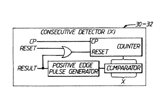
irst consecutive detector circuit 30 and the output of
AND gate ~3 (which i.5 high whenever the current address is
determined to lie inside the address block) is connected
to the reset terminal of circuit 30. The first
consecutive detector circuit 30 is shown in greater detail
in Figure ~.
As will be clear from Figure 3, circuit 30 is effective to
count the number of consecutive addresses which lie
outside the address block and will output a negative-
going pulse to the set input (S) of a first flip-flop
circuit 31 whenever this count reaches a first preset
threshola value tWhiCh is 20 in this embodiment).
Similarly, the clock pulse terminal (CP) of a second
consecutive detector circuit 32 is connected to the output
of AND gate 27 which goes high whenever the current
address is determined to lie inside the address block and
as having a value tYYY) less than the value (XXX) of the
reference address. Two further gates 33,34 ensure that
the second consecutive detector circuit 32 will be reset
if the current address is determined to have a value equal
to or greater than the value (XXX) or outside the address
block. Accordingly, the second consecutive detector
circuit 32 is effective to count consecutive output pulses
from gate 27 and will reset the first flip-flop circuit
2 ~ 7 ~
31 whenever this count reaches a second preset threshold
(which is three in this embodiment).
As already explained, the output oE AND gate 28 will go
high whenever the current addres<; is detected as being
exactly the same as the reference address Aref. In such
circumst~nces, the data switching circuit of the inter-
facing device is required to be activated to effect data
replacement, provided the processing unit of the computer
games console is operating normally; that is to say,
provided self-checking routines are not being carried
out. To that end, the output of AND gate 28 is connected
to one input terminal of an inverted-input AND gate 35.
Provided the inverted input of gate 35 is low the required
actuation pulse will be output onto line L, whereby to
trigger data replacement at the start of the next read
access cycle.
However, if, as will now be e~plained, it is determined
that self-checking routines are being carried out, a
cloaking signal CLOAX will be generated which causes the
inverted input of the gate ~5 to go high thereby
inhibiting the output of actuation pulses onto line L, and
preventing data replacement from taking place.
Different criteria may be applied to gauge whether or not
_ 15 -
2 0 9 6 6 7 ~
sel~-checking routines are being carried out, and the
cloaking signal needs to be generated.
In the described embodimcnt of the invention two different
criteria (which may be applied separately or in
combination) are adoptcd, and these criteria can be
selected by appropriately setting the values o two
control bits (A and B) applied to respective input
terminals of two further AND gates 36,37.
The outputs o~ AND gates 36,37 are connected to the
inverted input of gate 35 via OR gate 38.
If control bit ~ is set high, the cloaking signal will be
generated at the output o gate 38 whenever the output of
the first flip-flop circuit 31 is high, and, as already
e~plained, this will occur whenever the output of the
first consecutive detector circuit 30 goes high as a
consequence of detecting twenty consecutive addresses
lying outside the address block. Conversely, the cloaking
signal will be removed whenever the output of the first
flip-flop circuit 31 is low, and this will happen if the
second consecutive detector circuit 32 subsequently
detects three consecutive addresses which lie inside the
address block and have values below that of the reference
address Aref.
209~67~
With this scheme, selected by setting control bit ~ high,
the cloaking signal will be generated (thereby preventing
data replacement from taking place) if sustained activity
on the main address bus of addresses lying outside the
address block is detected. This condition is gauged by
detecting twenty consecutive addresses outside the address
block, and normal address activity i~ deemed to have
resumed upon detection of three consecutive addresses
which lie inside the address block and have values below
that of the reference address Aref.
In this way, data replacement should only ever be effected
if the program counter of the processing unit flows over
the address code immedlately preceding the reference
address and is turned off by sustained read activity
outside the address block.
If control bit A is set high, different criteria are used
to gauge whether or not sel-checking routines are in
progress and the cloaking signal needs to be generated.
In this scheme, the output o a yet further AND gate 23'
(which is high whenever the current address lies inside
the address block but does not equal the reference
address) is connected to the clock pulse input (CP) of a
counting circuit 39. The reset input of counting circuit
2~79~7~
39 is connected to the output of OR gate 40 whose
respective inputs are connected to thc outputs of the
irst and second consecutive detector circuits 30,32.
With this arrangement, the counting circuit will be reset
i~ the output of either consecutive detector circuit 30,32
goes high. Accordingly, if the counting circuit is not
reset, allowing the count to continue, this demonstrates
that the number of consecutive accesses outside the
address block is fewer than a first preset number (20 in
this example - i.e. the criterion set by circuit 30) and
that the number o consecutive accesses within the address
block is less than a second present number (3 in this
example - the criterion set by circuit 32).
Respective comparison circuits 41,42 compare the count in
counting circuit 39 with the valùe XXX of the eight low
value bits of the reference address Aref and with the
value XXX of the complement of the eight low value bits.
If the count reaches either value, one input of a
respective ~ND gatc 43,44 will go high. The other inputs
of AND gates 43,44 are connected to respective outputs o~
a second flip-flop circuit 45, whose respective set and
reset input ter~inals are connected to the outputs of AND
gates 28 and 29. The outputs of AND gates g3,44 are
connected to the inputs of OR gate 45 whose output is
connected to one input of AND gate 37, the other input of
- la -
jr! ~
gate 37 being connected to receive the control bit A.
With this arrangement, the cloaking siqnal will be
generated at the output of OR gate 3a provided the count
in circuit 39 reaches either of the aforementioned
threshold counts (XXX or XXX).
The value XXX of the eight low value bits of the reference
address Are~ represents the number of addresses in thc
address block lying below the reference address, ~hereas
the value XXX o the complement of the eight low value
bits represents the number of addresses in the address
block lying above the reference address.
Accordingly, wi~h this scheme, selected by setting control
bit A high, if the value of the count in counting circuit
39 reaches either of the afore-mentioDed values XXx or
XXX, this indicates that a check sum or memory checking
routine is flowing over the reference address either from
the bottom of the address block upwards (if the count in
circuit 39 reaches XXX) or from the top of the address
block downwards (if the value in circuit 39 reaches XXX~.
~he function of the second flip-flop circuit 45 is to
ensure that the associated input of the correct AND gate
43 or 44 is màintained high depending on whetheL the
detected addresses lie respectively below or above the
2~6 7~1
reference address.
The count in counting circuit 39 will approach the value
XXX or the value XXX as successive accesses within the
address block increment it. The afore-mentioned criteria
are based on the proposition that whilst check sum and
memory checking routines are in progress there are likely
to be fewer than the first preset number ~e.g. 20) of
address accesses outside the ad~ress block for every
access inside the address block and that there are likely
to be fewer than the second preset numbcr (e.g. 3) of
consecutive address accesses inside the address block.
European patent specification, publication No. 402,067
also discloses a data comparison technique whereby data
from the external memory is compared with latched reference
data which is the same as the data (from the e~ternal
memory) which is to be replaced by the replacement data
Drep. This additional comparison enables substitution
of the correct data and prevents errors that could arise
as a result of ambiguity in the process of comparing
addresses.
However, a problem may arise if the timing is such that
execution of the data comparison technigue involves a
delay which involves latching the data comparison result
~9 6 6 ~ ~
at an arbitary (unclocked) point in the processor's read
access cycle, which adversely affects the desired
operation of the system.
Furthermore, the data bus will contain data values derived
from several access cycles prior to the current access
cycle, and if these data values have been generated as a
result of check sum or memory checkinq routines they will
diFfer from the expected data values from the ext.~rnal
memory.
With a view to alleviatinq these problems, the embodiment
now described has the capability to generate a cloaking
signal, whereby to inhibit the replacement of data, in
response to a comparison of reference data and actual data
present on the data bus carried out during a read access
cycle which is earlier than the most recent cycle in which
such comparison is carried out, and this procedure
provides an additional or alternative means for detecting
check sum and memory checking routines.
To that end, the embod~ment shown in Figure 2 has a shift
register comprisinq the serial arrangement of two latches
46,47 which are clocked by the read access pulses on line
RA. The result To of a comparison of data carried out
during each successive read access cycle is input to the
- 21 ~~ 7 1
first latch 46 of the shift register and, as will be
apparent from ~igure 2, the efect of clocking the two
latches is to temporarily store the results To, Tl and
~2 of data comparisons carried out durinq successively
earlier read access cycles and to route each result to one
input o~ a respective AND gate 48,49,50.
The values of control bits C,D supplied to each AND gate
48,49,50 determine which o~ the three results
o' 1' 2 will be supplied to 02 gate 38 in
accordance with the following table.
C _ _ DEffec~
0 0No Cloaking Signal
1 0~To selected
Cloaking
o 1Signal if (Tl se~ected
1 1tT2 selected
By this means, data replacement can be rendered totally
insensitive to the results of the data comparison (C=O,
D=O~ or can be inhibited in response to data comparisons
carried out during a selected one of successively earlier
read access cycles.
It will be unders~ood that the two different techniques
embodied in Figure 2 (i.e. detection of self-checking
activity on the one hand and data comparison on the other)
2 ~
can either be used in combination (as is the case in
Figure 2~ or independently.