Note: Descriptions are shown in the official language in which they were submitted.
W O 92/09436 PC~/CB91/02093
20~7~
LAMINATE FOR USE IN MANUFACT~RE OF INX JET PRINTHEADS
This invention relates to ~ lsminate for use in th2
manufacture of printheads for drop--on-demand ink jet priDting.
In European Patent No. 0278590 the~e is described with
reference to Figures 2(a) and 2(b) a printhead structure of the
so-called "chevron" type. This is an advantageous form of
structure as it requires a relatively low operating voltage.
Further, United States Patent No. 5,016,028 discloses an array
printhead of the so-called "cantilever~ type which reguires a
relatively high operating voltage, in which manufacture takes
place from o~e side of the printhead.
One object o~ the present invention is to provide a
laminate for use in manufacture o~ an arrny printhead of the
chevron type so that manufacture thereof can ta`ke place from one
side of the arr y.
The present invention consists in a co-fired laminate
for use in the manu~acture of printheads ~or drop-on-demand ink
jet printers, comprising two inner layers of pie~o-electric
cersmic material which ~re thickness poled in opposite senses and
two outer layers of inactive ceramic material, charscterised in
that between said inner layers is provided a fifth layer of
ceramic materi&l which in response to actuating pulses at the
operating temperature of the printhead is substantially
insulating and at the poling temperature of the inner layers is
substantially conductive during the poling period.
.
.
.. - .. . .. . . ..
W O 92/09436 PC~/G~91/02093
n,, ~ ) 2 -
S~itably, the resist~nce of said fifth layer lies in a
range of approximately l.5 orders of ~agnitude. Preferably, the
resistance of the fifth layer lies between 75 M.ohms/square and
2500 M.ohms/square at 60C.
In one form of the invention said fifth layer is a
negative temPerature coefficient (~C) ceramic ~aterial having a
critical temperature between the operating and poling
temperatures at which the resistance of ~aid material changes
rapidly.
In a further form of the lnvention said ou~er layers
sre formed of an insul~ting cera~ic. Said cer~mic suitably is a
glass ceramic ~nd m~y be formed with a dopant to increase the
conductivity thereof at the poling temperature.
The invention further consists in the ~ethod of forming
a ~rop-on demand ink jet array printhead comprising
(a) forming a co-fired laminate having two inner layers
of piezo-ele~tric material, two outer layers of inactive ceramic
material and a ~ifth layer of ceramic ma~erial between said inner
layers which is insulating in response to actuating pulses at the
operating temperature and at the poling temperature is conductive
during the poling period;
(b) applying electrodes to outer surfaces respectively
of s~id two outer layers;
(c) applying a poling pulse between said fifth layer
and said electrodes thereby to e~fect thickness poling of the
inner l~yers in respectlve opposite senses;
'
- , ~ , . . - . . , . . , ,.. , . -
~ .
.. .
W O 92/0'9436 2 0 9 ~ 7 2 6 PCT/GB~l/02093
(d) removing one of the ~uter layers;
(e) forming an array of parallel channels of depth
which extends normal to the laminate through the inner layer from
which said one of the outer layers was removed, the middle layer
and a substantial part at least of the other of said inner
layers; and
(f) applying electrode layers to facing sides Or each
of said chsnnels.
The invention will now be described, by way of example,
with reference to the accompanying drawings, in which:-
FIGURE 1 is a cross-~ectional vie~ of a laminste
according to the invention;
FIGURE 2(a) and 2(b) are cross-sectional views of the
laminate of Figure 1 in the course of conversion thereof to an
ink jet array printhead component;
FIGURE 3 is a diagram of electrical resistance per
square of the central layer of the laminate oP the earlier
Figures against temperature. It illustrates the ~rend o~ the
min1mum resistance appropriate for shear mode wall actuation of a
chevron-type of channel wall actuator at room temperature and the
trend of the msximum resistance ~uitable for poling the laminate
at the poling tempersture;
FIGIRE 4 is a diagram similar to that of Figure 3
showing the variation of electrical res1stance per square against
temperature of the central layer of the laminate when ths central
layer compri~es a negative temperature coefficient material.
.
W O sZ/09436 PC~/Gn9l/02~93
~ ~ 9 6~1,6 _ 4
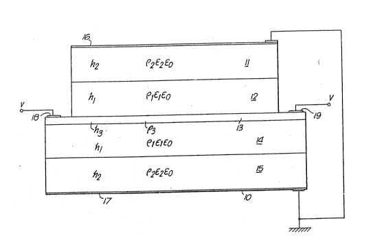
Referring first to Figure 1, a laminate 10 comprises
five layers 11 to 15 each o~ which is a ferro-elec~ric ceramic.
Suitably, each of the layers is -tape-cast in the form of
longitudinal strips pres3ed onto one ~nother and co-Plred.
Outer layers 11 and 15 of the laminate are of lnactive
materials sultable for being co-fired wlth inner layers 12 ~nd 14
of piezo-electric ceramic made o~ lead zircon~um titanate (PZT).
The preferred materials for the inner layers are a
polycrystalline PZT having superior piezo-electric activity
defined by the property (dl5/ rD55) such as is obtained from
Motorola D3203 or Tokin N-8, N-10 or N-20. These are
commercially available msterials having high shear mode
activity.
The outer layers 11 and 15 may also be of
piezo-electric ceramic with thermal expansion characteristics
matched to those o~ the inner lAyers and haYing similar or the
same basic mix as is used for the inner layers but also including
a dopant to render the ceramic inactive or depoled when subject
to an electric field. An example of a suitable dopant is
lanthanum (La) or Strontium (Sr). The addition or substitution
of Lanthanum for exa~ple is known to depress the Curie
temperature o~ the material. By the addition o~ 5 - 10X o~ such
dopants the material of the outer layer~ is readily depoled by
raising the temperature of the laminate to their Curie
temperature, while the material o~ the~inner layers re=ains
polarized. With addition of sufficient dopant, the Curie
.
~-
' .
- , ,, . ,,, ,:
"/0 92/09436 PCI/CB')1/020~3
20~67~1~
temperature can be depressed below the poling temperature and in
this case the outer layers will never become poled. The laminate
is symmetrical, so that is not liable to distort under poling or
depoling stresses and uch stresses rapidly decay by creep. A
satisfactory effect ~s regards rendering the outer layers
inactivs or depoled when subject to ~n electric field may be
obtained with concentrations of dopant in the range 2 to 25%.
The central layer 13 is a thin layer of doped ceramic,
which may be applied optionally in tape cast form, or as a slurry
which is coated on one of the facing surfaces of layers 12 and
1~ .
The laminate is subsequently fir0d and poled as
described below. Channels sre then cut through layers 12, 13 and
14 and operatlng electrodes deposited onto channel separating
side walls as are shown in FIG. 2 and described hereinbelow in
the detailed discussion of manufacture of the printhead.
Lsyer 13 is effectively insulating in response to the
operating waveform, typically pulses of 10~ seconcls duration, at
the operating temperature (0-60C) of the ink jet printhead but
is substantially conducting on application of the pollng voltage
pulse, typically of 10 seconds duration, ~t the poling
temperature. It is a preferred aspect of this layer that it is
characteri7ecl by a temperature coefficient of resistance of
negative slope, so that its conductivity incre~es as temperature
increases. ~is is characteristic of ceramic materials and
thermistors, but is the opposite of the characteristic of
metallic concluctors whose resistance incre~ses wl~h temperature.
- - :' .
..
; , '; ~ ~ ' ' '
.
'
W O 92/09436 PcT/GB9l/o2o93
~ 96r~
The condition that the layer 13 i~ effectively
insulating in response to the operating waveform at the operating
temperature applied to the electrodes of ~n actuator i5
quantified by reference to Figure 2 ~nd illustrated in Figure 3.
If the period of the waveform is 10 usec and the charge le~kage
through the layer 13 in the actuator i~ limited to 1%
1 ~ 3 ~l~o ~ 10 5 = 10 3
3 10
where hl is the thic~ness of each layer 12 or 14
h3 is the thickness of layer 13
~1 and ~O are respectively the relative permittivity
of each layer 12 snd 14 and of free space, and
~ 3 is the resistivity o~ layer 13.
and, if hl = 250xlO 6m ~1 = 3 ~O = 8.85xlO 12 F.m 1
the layer resistance
per square ~ 3 106.10 3
= 76 M.ohm per square
h3 2x250x3000x8.85xlO 12
The condition that the layer 13 is subst~ntially co~ducting on
application o~ the poling voltage pul~e can also be quantified.
The poling voltage ~ illustrated in Figure 1 is applied to
electrodes 18 ~nd 19 on each side of the strip at the poling
temperature, typically 120C. Charge then flows inward
through the layer 13, so that the d~fferential voltage between
the layer 13 and the electrod-s 16 snd 17 becomes
: - - ~ , : ,
. .
W O 92/09436 PCT/~,B')I/02093
2~72~
-7-
progressively uniform. Typically, it is required to attain 99~
uniformi~y between the voltage at the outer edges and that at the
centre of the strip within a poling pulse period of 10 secs.
Analysis shows that the voltage distribution is
expressed by a simple diffusion equation of the form
a2v = ~o 3 . ~V
~X2 h1 ~ h2 ~t
~1 ~2
and that 99% uniformity is attained when
~ ) . t where ~ = X
h /2
3 2~o (~/2) 2
'
and i~ ht = h2 = 250 x lO 6m ~ = 8.85xlO 12 F.m 1
~i ~2 3000 t = 10 sec ~ = 4Omm
where hl = h2 is the thickness of each layer 11 and 15
V is the poling voltage
is the distance between the electrodes 18 and 19
t is time for the voltage in the layer 13 to become
99 percent uniform and is s the poling time.
0 x 2 x 250 x 10-6
3 <
3000 x 2 x 8.85 x lO 12 x 400 x lO 6
: e 3 < 220 M.ohm per square
.
W 0 92/09436 PCT/~B')l/02093
9 ~
The conditions that~3/h3, which i~ the resistance
per square of the lsyer 13 > 76 M.ohm at the operating
temperature of 60 C and that~3/h3 220 M.ohm at poling
temperatures of 120 C and 180 C are~ illustrated as line~
marked C and D in Figure 3. Measured at 60C, this r~n~e is
between 76 and 2500 M.ohm per square.
In Figure 3, the resistancep3/h3 per 4quare is
plotted over five decades fromp3/h3 = 1-105 M.ohm, over a
temperature range 0-180C.
I'he resistance of ceramics is characterized by a
temperature coefficient of negative slope and of magnitude such
that the resistance typically falls by an order of ~agnitude for
every increase in temperature of 60C.
The line A indicates the course of the resistance per
square~3/h3 of layer 13, such that at 60C its resistance
per square = 76 M.ohm. In that case 1% of the charge stored a~
60C is discharged during the operating cycle. The line B
indicates a lower resistance per sguare when 10% of the charge
stored at 60C is discharged during the operating cycle. For
practical operation the resistance per square of layer 13 should
be to the right of line A.
Similarly the line C is such that the resistance per
sguare is 220 M.ohm at 120C. In that case the poling field is
99X uniform after application for 10 seconds. The line D
indicates~the resistance per square ~or a material poled with
similar uni~ormity at 180C. In practice the material selected
should be to the left of line C.
'
.
W O 92/09436 PCT/~B91/()2093
20~'~72~
_ 9 _
.,
The material of layer 13 should thus be selected to
have a resistance per square in the range between lines a and C
i.e. within A resistance ra~ge of about 1.5 orders of nagnitude,
this range being obtained by readi.ng the ~eparation of the line~
A and C at the ssme temperature.
The~e calculations indicate that a resistance per
square ~3/h3 of layer 13 can be abtalned ~uch that it 1~
effectively insulating in response to the operating wave~orm
(lO~ec) at the operating temperature (0-60C) of the ink jet
printhead, but is substantially conducting on applicatlon of the
poling wave~orm at the poling temperature (of 120-180C) for a
duration of 10 seconds.
The material of layer 13 may however be a material
comprising an NTC (negative temperature coefficientj ceramic.
NTC ceramics are materials having 8 non-llnear variation of
resistivity, such that their resistance undergoes a st~p
reduction with~n a narrow temperature range. Nor~ally this step
change of resistivity is limited to 1-2 orders of magnitude
concentrated over 5-10C ra~ge. If this critical temperature
is chosen to be above the operating temperature and below the
poling temperature, the margin of resistance per square is
further incre~sed above that indicated in Figure 3 for a ceramic
insulstor.
This is illu-~trated in Figure 4 where the chain dotted
lines A' and C' show the corresponding limiting valves of
reslstance per square with temperature under operating and poling
canditions respect.ively ~or an NTC ceramic. The effective
1:
,
WO 92/09436 pcr/G B') 1/02093
9 ~ 6 lo -
temperatures are the operatin~ and poling temperatures, typically
60C and 120C, and the resistance per ~quare range is no~
around 2.5 orders of magnitude, this range belng that between the
locations at which the lines A' and C' lnter3ect either of the
said typical operating and poling l:emperatures. This range
affords increased margin in the chc~ice o~ resistlvity per sguare
of the layer 13.
The outer layer 11 ~nd 15 in an alternative form of the
invention may be an insulating ceramic, such as a glass cera~ic,
chosen to have a thermal exp~nsion coefficient matched to that of
the layers 12, 13 and 14. Examples of such a material are
Cordierite and oxides of Lithium Aluminium and Silicon which are
glass cera~ics whose expansion coefficient can be selected
according to ingredients and thermal history to lie in the range
of 1-4 x 10 6 per C. Such a material can be co-fired with
the pie~o-electric layers 12-14 and has the advantage that its
i modulus of elasticity is greater than the materials described
above, which were La or Si doped PZT~
The dielectric constsnt of a glass ceramic such as
cordierite is usually 8-12 and is thus substantially lower than
that of layers 12 and 14 where ~1 is typically 3000. As will
be evident later the poling voltage to pole layers 12 and 14
through layers 11 and 15 respectively is made substanti~lly more
difficult due to its lower dielectric constant. Conseguently,
the resistlvity of the outer layers 11 and 15 if they consist of
glass ceramic is reduced by the addition of dopants.
. .
- . , - ~
W O 9~/09436 PC~'/C~'Jl/02~3
209672~.~ '
Typically, the resistivity ~2 of layers 11 ~nd 15 i5
reduced so that
p2 < hl t
h2 ~l~o
and if ~1 = 3 ~O = 8.85 x 10 12 F.m 1
and t = lOsecs h - h
~2 < 3.8 x 10⁸ ohm.m
then the voltage applied to the outer electrodes 16 snd 17
penetrates layers 11 and 15 respectively during the 10 second
period o~ the poling pulse, and a high proportion of the voltage
is effective over the piezo-electric layers 12 and 14 because
charge penetrates the layers 11 and 15 by conduction 50 that the
voltages at the interfaces o~ the layerQ 14 and 15 and the layers
11 and 12 tend to become egual to the voltage oP the electrodes
16 and 17 respectively.
~ Thus layers 11 and 15 ~ay option~lly be made oP an
insulsting c~eramic, providing its resistivity is suitably reduced
at the~poling temperature. This ~spect was disclosed in United
States Patent No. 5,035,24i.
~ ,.
,, ~ ~ ' , .' . . : . ...
W O 92/09436 PCT/GB91/02n93
'~ 9 ~ 6 _ 12 ~ ~
The laminate 10 may be made as previously stated from
five layers of ceramic of suitable materials that are tape csst,
pressed together and co-fired, the fifth being optionally applied
as a slurry to one of the Pacing s~rfaces of the liner layers 12
and 14. The laminate includes outer electrode~ 16 and 17 and
central electrodes 18 and 19 formedl on either slde of layer 13.
During firing, due to the symmetry of the laminate~ the ceramic
remains substantially flat.
The laminate is poled by appllcation of a poling field,
as illustrated, between electrodes 16, 17 and 18, 19. This
applies a poling field to polarize the piezo-electric material of
layers 12 and 14 in a configuration denoted by arrows indicated
in Figure 2. If layers 11 and 15 comprise a piezo-eIectric
material, and they become polarized during the poling step, they
are readily depoled by heating them above their Curie temperature
during or after poling: if ehose layers ~re an insulatlng
ceramic which is non piezo-electric, an enhanced conductivity in
those layers helps to limit the magnitude of the poling ~ield.
A~ter poling, the materia]s are aged to allow residual stresses
to relsx by creep. Nor~al ~ctivity tests of the piezo-electric
structure can be-performed to monitor the material
ch~racteristics.
The construc~ion of an ink ~et printhead component from
the laminate is illustrated by reference to Figures 2(a) and (b)
in which the five layers are shown diagrammatically on the left.
Initlally the layer 11 and its electrode 16 are removed by
grinding or lapping and the lower electrode 17 is removed by
, : , , - ., , : :. ... .. -, ~ ~. , - : -
W O 92/09436 PCr/GJB9l/02093
20~672~) '
- 13 -
lapping or etching leaving the face so exposed of layer 12 and
layer 15 parallel and the sur~ace of the layer 12 flat to 8 high
tolerance.
Ink channels 20 are then cut in the laminate as
illustrated in the centr~l ~ection. The method of for~ing
channels has previously been disclosed in Unlted States Patent
No. 5,016,028 which relates to an ink ~et array printhead which
can be manufactured from one side of the channel structure.
However, because the layers 12 and 14 are oppositely poled
the wall actuators will now be of the so called "chevron" type,
such as are the subject of European Patents No. 0277703 and No.
0278590. These actuators are known to be advantageous because
they require a lower actuating voltase to establish the same
preQsure in the ink channels during operation. If the insulating
glass ceramic is u~ed in the layer 15 thi~ serves to stif~en the
wall actuators Qt their root interface with layer 15, which also
serves to limit the co~pliance of the wall actuator.
After for~ing chnnnels as illustrated in Figure 2(b)
the wall actuators Rre plated with electrodes 30 as illustrated
in the right hand ~ection to which ~ psssivation coating may be
applied. Subsequent operations to build an ink Jet array
prlnthead are _OWD in the urt-
,
--
: : - . :
' ' ' . ' " ' ~ ' . ~ .
.