Note: Descriptions are shown in the official language in which they were submitted.
W~?2/12219 PCr/U592/Onl73
.. ~ :
1 2~9~g26
POLYNER~DI~R~ED LIQ~ID CRY8TAL DEVICE
~AVING AN UhT~AVIO~ET--POI~ IZABIIIS MATRIX
aND A VARIAPI.E CIPTICA~ TRA11~2~I88ION
AND A I~ HOD FOR PRBPARING ~115 8A~E
~echnical Field
This invention relates to a
polymer-dispersed liquid crystal device (hereinafter
referred to as a "PDLC device") and, more
particularly, to a PDLC device which is based on an
ultraviolet polymerizable matrix. Devices according
to the invention display a selectively adjustable,
variable transmission of specular light as a function
of applied voltage. This invention also relates to a
method for preparing PDLC devices generally.
.
Backqround
PDLC devices generally comprise droplets of
a biaxially birefringent, nematic liquid crystal
material dispersed in a transparent polymeric matrix.
PDLC devices are of interest because they can be
electrically controlled or switched between
relatively translucent (i.e. light scattering) and
relatively transparent (i.e. light transmitting)
states. This occurs because the liquid crystal
droplets exhibit birefringence. As a result, the
droplets strongly scatter light when they are
randomly oriented in the matrix and the PDLC devices
appear translucent. However, upon the application of
either an electric field or a magnetic field, the
droplets become aligned along the direction of the
el~ctric/~agneti- fi_ d vcc,o. a..d m~,c direc.ly
transmit light. Alternatively, the droplets can be
.
,-, : '
. ~ .
WO92/12219 PCT/US92/001 ~
~0~6~2&
thermally stressed to induce alignment.
If the refractive indices of the liquid
crystal material and the polymeric matrix are closely
matched while in the field-induced, aligned state,
the devices appear transparent. Thus, upon the
application of an electric field, a magnetic field,
or a thermal stress, PDLC devices switch from a state
in which they appear translucent to a state in which
they appear transparent. Upon removal of the
electric field, the magnetic field, or the thermal
stress, the devices revert to a translucent state.
PDLC devices are sometimes described as
being switchable between opaque and transparent
states. Strictly interpreted, the description of
PDLC devices in the "field-off" state as "opaque" is
not correct. However, the terms "opaque" and
"translucent" have apparently been used synonymously
and there seems to be no significant misunderstanding
regarding the functional appearance of the devices.
More accurately, PDLC devices in the field-off,
nonaligned state transmit light, but the light is
dispersed to the extent that images viewed through
the devices appear cloudy or diffuse. That is, the
PDLC devices are translucent. Truly "opa~ue"
devices do not transmit light.
PDLC devices have found use as light
valves, filters and shutters. The devices have also
been used in information display arrange~ents where
it is desirable to have a sharp, rapidly achieved
contrast between the translucent and transparent
states for addressing purposes such as is required
for ~ultiplexing. ~y "Sha~" it is ~eant that the
devices experience a substantial change in the
percentage of light incident upon the device which
' ' ' ' ' ~ ' ~ : !
,` . . . . .
' . ~ ' ' : '
-' ~ '' ' ' ' ` ' ,
'
W092/12219 PCT/~S92/00173
3 2~9~2~
can be specularly transmitted therethrough for a
correspondingly small change in the amount of applied
voltage. That is, a small change in the voltage
(e . g., a change of less than lO volts) applied to the
device causes the device to switch between the
transparent and translucent conditions. By "rapid" it
is meant that the time required for the device to
switch between the transparent and translucent states
is very short (on the order of milliseconds).
It is an objective of most presently known
PDLC devices to exist in only one of two extreme
states ~either translucent-off or transparent-on).
These devices do not provide a uniform, variable
optical transmission or variable grey scale.
Furthermore, these PDLC devices cannot be varied and
selectively adjusted from, at one extreme, a
translucent off-state (corresponding to about 0~
relative transmission) to, at another ext.eme, a
transparent on-state (corresponding to about 100%
relative transmission) with an infinite number of
intermediate, preferably uniform, ~pecular light
transmission levels in between. This inability to
provide an infinite number of intermediate light
transmission levels is believed to be due, in part,
to the objective that the devices switch sharply
(i.e., over a small change in voltage) between the
translucent and transparent conditions. Thus, the
devices tend to exist only in these extreme states.
Variable grey scale PDLC devices would be
useful in numerous applications. If provided in the
form of thin, flexible sheets, the devices could be
applied to moto~ vehi~le ~--n-oo-s cr side wi..~o~-s so
that occupants of the motor vehicle could adjust the
PDLC device to regulate the amount of specular light
,
. . : : ~, .
, ... . ~...
. .
W092t12219 PCT/US92/OOt7
passed therethrough. Similarly, the devices could be
applied to architectural windows, sloped glazings, ~ -
skylights, interior glass partitions and the like to
provide glare and/or privacy control for occupants of
the building.
PDLC devices and methods for preparing them
have been described both in the scientific and patent
literature. For example, a device which suggests a
variable grey scale is disclosed in U.S. Patent No.
4,749,261 to McLaughlin et al. and assigned to Taliq
Corporation. This patent dlscloses a shatterproof
liquid crystal panel which comprises a pair of
transparent boundary surfaces formed of glass or
plastic with nematic curvilinearly aligned phase
("NCAP") liquid crystal material disposed
therebetween. The NCAP liquid crystal material
comprises plural volumes of an optically transparent
liquid crystal formed in an optically tzansparent
containment medium such as a polyvinyl alcohol or a
latex. The volumes of liquid crystal material may
be separate from one another, may be interconnected
to one or more volumes, or may include both separate
and interconnected volumes. The liquid crystal
material may be prepared as an emulsion of liquid
crystal and containment medium, the emulsion being
subsequently dried (i.e., cured). Alternatively, the
liquid crystal material may comprise a plurality of
individually formed capsules of liquid crystal in a
containment medium. The panel further includes a
pair of electrodes and a variable element which can
adjust the magnitude of an electric field applied to
the liquid crystal ~aterial. P.epor~edly, by vii-_ying
the magnitude of the electric field applied across
the liquid crystal material, the extent to which
. .
,. . , . i.
:~ :
W0~2/12229 PCT~US92/00173
5 2~9~826
light is transmitted through the panel may be varied.
The NCAP liquid crystal materials of the
McLaughlin et al. patent are made by an emulsion or
encapsulation technique which is described more fully
in U.S. Patent No. 4,435,047 to Fergason. Emulsion
or encapsulation typically involves emulsifying a
liquid crystal material with an aqueous phase
containing the encapsulating medium, spreading the
emulsion onto a substrate, and allowing the aqueous
phase to evaporate. Such systems are sensitive to
moisture degradation and demand the use of relatively
thick, spacer-separated substrates which can be
easily coated. For example, FIG. 4 describes a
liquid crystal display device which includes a
substrate having a thickness of about 10 mils,
(including an approximately.200 angstrom thick first
electrode), a liquid crystal/encapsulating medium
layer approximately 1 mil thick, and an approximately
0.5 mil thick second electrode. Because a water
soluble polymer or a polymer emulsified and dispersed
in water is employed, the structure presumably has
limited water resistance.
The moisture sensitivity of such devices is
considered in U.S. Patent No. 4,992,201 to Pearlman
which proposes, as a solution to this problem, that
the liquid crystal material be dispersed in a latex
medium, the latex medium being obtained by drying a
suspension of natural rubbers, synthetic polymers or
synthetic copolymers. The liquid crystal/latex blend
may be coated onto a substrate and dried.
on the other hand; PDLC devices, such as
those discl^sed hereir. ir.vol.e pol,~r.zation~ c2d
phase separation, a technique which offers certain
advantages over the emulsion or encapsulation
. . ~ . . , :
.. . ,... , ~ : . .
WO92/12219 PCT/US92/0017~ ! `-
2~9682ti - ~
process. Polymerization-induced phase separation is
a solvent-free approach which results in the
formation of structures which are less moisture-
sensitive. Also, polymerization-induced phase
separation allows for the production ~f higher
molecular weight matrices which have enhanced
structural properties so as to impart certain desired
characteristics to the matrix.
In polymerization-induced phase separation,
liquid crystal microdroplets spontaneously form in a
polymer matrix upon the separation of the liquid
crystal and matrix phases. Phase separation is
induced by causing the uncured matrix material to
polymerize. A polymerization induced-phase
separation in which the uncured matrix material
polymerizes upon exposure to ultraviolet (W)
radiation is particularly desirable because these
systems are easily handled, do not require two-par~
formulations (as do epoxy-based systems), and because
the phase separation kinetics can be readily
controlled by adjusting the process parameters.
An early report of polymerization-induced phase
separation is found in U.S. Patent No. 3,935,337 to
Taylor. More recently, U.S. Patent No. 4,728,547 to
Vaz et al. disclosed an optically responsive film
comprising li~uid crystals dispersed in an W -curable
polymer matrix. Liquid crystal/matrix material was
applied between a pair of 20 micron (~) silica
microsphere-separated glass plates and then exposed
to W radiation. W -curable polymer matrices
include those based on thiol-ene chemist~y. PIG. l
of the Vaz et al. patent suggests that within the
polymer matrix, a uniform distribution of equally
.,, . , - ~ - . . . .
.
,:
' . ' ' ', '. ' ~ " . " '.' , . ~:, ', . '
W O 92/12219 PC~r/US92/00173
2 ~) 9 ~o 8 2 ~ .
sized liquid crystal microdroplets is desirable.
Reportedly, the liquid crystal microdroplets should
be about o.l to lo ~, preferably 0.5 to 1 ~ in
diameter. High intensity W radiation was used to
cure the liquid crystal/matrix system (6 seconds of
exposure 3 to 4 inches from a 300 Watt/inch mercury
discharge lamp). The film may be used for
information displays, light shutters and the like,
applications for which a variable grey scale would be
undesirable.
U.S. Patent No. 4,834,509 to GunJima et al.
discloses an optical device in which liquid crystal
material is uniformly dispersed in a vinyl group-
containing matrix that may be polymerized with W
energy. The liquid crystal/matrix blend is
disposed betwsen a pair of electrode-bearing
substrates. The patent suggests that mechanical
spacers (e.g., glass, plastic or ceramic particles~
may be desirably employed to carefully control the
distance between the substrate electrodes thereby
minimizing irregularities in light transmission due
to coating thickness. The devices are useful as
large area displays, light controllers and light
shutters, applications for which a variable grey
scale would be undesirable.
U.S. Patent No. 4,~88,900 to Doane et al.
and assigned to Xent State University discloses a
light modulating material comprising liquid crystal
droplets dispersed in an epoxy or a polyurethane
matrix. The light modulating material is disposed
intermediate a pair of substrates. The matrix is
cured in a phase sepa_at-^n pr^^ess either thermai y,
upon exposure to W light eneryy, or with a chemical
promoter. Relatively thick structures in which the
.
WO92/12219 PCT/US92/~0173
~9~82~ 8
boundary layers (substrates) are separated by spacers
and in which equally sized spherical liquid crystal ~-
droplets are uniformly dispersed in the matrix are ~-
provided.
Thermally-cured epoxy-based polymer '
matrices are also disclosed in U.S. Patent Nos.
4,673,255 and 4,685,771, each to West et al. and each
assigned to Kent State University. None of the
aforementioned patents assigned to Kent State
University is known to exhibit a uniform, selectively
adjustable, variable grey scale but rather are useful
in information displays, light shutters, and the
like.
U.S. Patent No. 4,944,576 to Lacker et al.
discloses a PDLC device in which microdroplets of a
liquid crystal material are dispersed within a
photopolymerizable matrix material. The liquid
crystal/matrix blend was applied between a pair of
spacer-separated, electrode-coated substrates and
cured with W radiàtion. ~n electric field, a
magnetic field or a mechanical stress is applied
during photopolymerization to partially align the
liquid crystal microdroplets. As a result of this
partial alignment, the PDLC device performs similarly
to known devices but with lower threshold and
operating voltages. Lower threshold and operating
voltages are typically associated with a sharp
transition between the translucent and transparent
states which is supported by the failure of FIG. 4
(graphical plots of % transmission v. lO0 Hz Signal,
rms volts (i.e., voltage)) to describe a variable
grey sca~e PL~C devico.
U.S. Patent No. 4,938,568 to Margerum et
al. discloses various PDLC devices comprising
.. . ~, . . ~. ~ . .. .
WO92/12219 PCT/US92/00173
2 ~ 9 6 ~ 2 D
microdroplets of a liquid crystal material dispersed
in a photopolymerizable matrix and applied between a
pair of electrode-coated, spacer-separated
substrates. ~y controlling the conditions of
photopolymerization, Marger~m et al. can create a
variation in the size of the liquid crystal
microdroplets. Reportedly, several different types
of PDLC films may be obtained by spatially varying
the conditions of polymerization over the film so
that the sizes of the liqui~ crystal droplets are
also spatially varied. In one approach, the exposure
intensity is spatially varied by exposing the film
through a mask which has a spatial variation in
transmissivity. The mask may be at least partially
transmissive over its entire area, thereby enabling
substantially the entire film to polymerize at about
the same time, but at spatially varying
polymerization rates corresponding to the spatial
variation in mask transmissivity. Alternatively,
polymerization may take place in a two-step process
by an exposure with the mask in one step, and an
exposure without the mask at a different exposure
intensity in another step. This technique is based
on the observation by Margerum et al. that liquid
crystal droplet size may be reduced by increasing the
intensity of the W radiation.
A representative structure is shown in FIG.
3 which illustrates alternating bands of "large" and
"small" liquid crystal droplets which repeat from one
edge of the PDLC film to the opposite edge. An -
alternative structure is shown in FIG. 5 which
sche~atic2lly illustrates a ~riaticn in 1 qui~
crystal droplet size through a PDLC film from one
major planar surface to the other. The resulting
WO92/~2219 PCT/US92/001 ~ ~
~0~6826 lO
PDLC devices have reduced operating voltages relative
to those previously known. A reduction in operating
voltage is typically associated with a sharp
transition between the transparent on-state and the
translucent off-state. Consequently, this patent
does not disclose a PDLC device which exhibits a
variable grey scale.
U.S. Patent No. 4,411,495 to Beni et al
discloses a refractive index switchable display cell,
lo the opacity of which may be varied by changing the
amplitude of an electric field applied across the
device. The cell comprises a preformed, commercial
porous filter imbibed with a liquid crystal material.
(A similar device is disclosed in "New display based
on electrically induced index matching in an
inhomogeneous medium" ADP1 . Phys. Lett. 40(1),
January 1, 1982 (pp. 22-24) by H. G. Craighead et al.
The preformed filter serves as a spacer and the
device is described as "providing a gray scale.")
Interest in PDLC devices has spawned a
spate of technical and academic articles. For
example, "Response Times and Voltages for PDLC Light
Shutters," Liquid Crystals, 1989, Vol. 5, No. 5, pp.
1453-65 by B-G. Wu et al. notes that the type of
polymer matrix can dramatically influence the
switching voltage (the applied voltage differential
required to transition the PDLC device between the
translucent off-state and the transparent on-state).
A PDLC device employing a poly(methyl methacrylate)
matrix may have a switching voltage of about 200
volts ~V), while an identical device reportedly
hzving the szme droplet s z2 and shap2 but using an
epoxy matrix may have a switching voltage of 20 V.
These observations were based on a system using a
.... - ,; ., , . ~ . ~ , ' ' . . .
. .~ . . . :: . ~ . : : . : :. :
, . , : :
- : , ~ . ~ . , ,
WO92/12219 PCT/US92/0~173
~9~26
liquid crystal material and poly(methyl methacrylate)
in a 1:2 ratio by weight. The mixture was applied
between a pair of spacer-separated, electrode-coated
substrates.
"Droplet Size Control in Polymer Dispersed
Liquid Crystal Film~," SPIE, Vol. 1080, Liquid
Crvstal Chemistry PhYsics and Applications (1989),
pp. 53-61 by A. M. Lack~er et al. teaches the
formation of PDLC devices comprising liquid crystal
droplets dispersed in an W -curable thiol~ene matrix,
the liquid crystal/matrix system being applied
between a pair of spacer-separated, electrode-coated
substrates. Liquid crystal droplet size was reduced
by increasing the intensity of the W radiation. At
an intensity of approximately 13 milliwatts/sq. cm
(mW/cm2), a droplet diameter of about 1.0 ~ was
achieved. The PDLC devices are not reported as
exhibiting a variable grey scale.
"A Light Control Film Composed of Liquid
Crystal Droplets Dispersed in an W -Curable Polymer,"
Liquid Crystal, 1987, Vol. 146, pp. 1-15 by N. A. Vaz
et al. discloses a PDLC device co~prising submicron
size liquid crystal droplets uniformly dispersed in
an W -curable matrix. The photomicrograph of FIG. 1
appears to show liquid crystal droplets of
substantially equal size. The liquid crystal/
uncured matrix ~aterial is disposed between a pair of
spacer-separated, electrode-coated substrates and
cured by exposure to W radiation of 85 mW/cm2
intensity (50% uncertainty). PDLC film thickness
was typically 27 to 30 ~. The devices are useful
for displays a~d light ~hutters ~u' do not other~ise
exhibit a variable grey scale. The discussion on
pages 6 and 7 of the article suggests that the
: . . : , .
': ' ' ': . .' ' : ! ' .
.. . ., . . . . .
WO92/12219 PCT/US92/0017
209682~ 12
performance of the device illustrated in FIG. 2 has
not been optimized and that it would be desirable to
have a sharper transition (i.e., the transition
between the translucent off-state and the transparent
on-state should occur over a smaller voltage range).
"Morphological control in polymer-dispersed
liquid crystal film matrices" by F. G. Yamagishi et
al., SPIE Vol. 1080, kiquid Crystal Chemistrv.
Physics and Applications (1989), pp. 24-28 discloses
the preparation of a PDLC device comprising liquid
crystal droplets dispersed in a polymerizable matrix.
The liquid crystal/uncured matrix blend was applied
between a pair of electrode-coated, spacer-separated
substrates and cured using W radiation in the range
of 60 mW/cm2. Some of the devices obtained by
Yamagishi et al. displayed a "polymer ball"
morphology in which domains of a polymeric material
are underst~od to be dispersed in a continuous liquid
crystal phase. There is no indication that any of
the resulting devices which comprise liquid crystal
droplets dispersed in a polymer matrix exhibit a
variable grey scale.
It is desirable in certain applications to
have PDLC devices which display a variable grey
scale. Presently known PDLC devices which suggest
the possible objective of a variable grey scale
employ emulsionlencapsulation formation techniques;
however, these techniques suffer from certain
undesirable limitations. The formation of PDLC
devices using phase separation and an
W-polymerizable matrix is advantageous. However,
presently known PDT~C devices which maXe use ol suc~
techniques do not exhibit a variable grey scale.
Consequently, there is a need for a ~DLC device which
-.: . , , . - . ,,
, . - . .
. . : . ,.
,
: - ~ .
WO92/12219 PCT/US92/00173
13 209 ~ 82~i
exhibits a variable grey ~ale and which employs an
W -polymerizable matrix.
Moreover, in the presently known methods
for producing PDLC devices based on an W-
polymerizable matrix material, the matrix material i5typically cured (polymerized) by exposing the uncured
matrix material to relatively high intensity W
radiation sources, for example, medium or high
pressure mercury or mercury/xenon lamps. Such
radiation sources can become quite hot during
operztion, necessitating the use of elaborate and
expensive cooling and temperature control systems.
Such radiation sources have also been associated with
certain maint~nance problems. Accordingly, it would
be desirable if PDLC devices could be produced in a
method which utilizes relatively low intensity W
radiation to c~re the uncured polymer matrix
material.
Disc~sure of the Invention
The invention relates to a
polymer-dispersed liquid crystal device which
comprises a multiplicity of droplets of a
birefringent, functionally nematic liquid crystal
material dispersed in a matrix which comprises the
reaction product of ultraviolet radiation
polymerizable materials. The device specularly
transmits incident light as a function of the
magnitude of an electric field applied across the
device and has a delta V ~" V") greater than or equal
to 15 volts (V). ~V may be calculated according to
the following equations:
~ V=(v80+0) - (V20+0)~ wherein V~O+O is a first
applied voltage corresponding to a first percentage
WO92/12219 PCT/US92/0017~
2~9~2~
14
of the total incident light transmitted by the device
as specular light, and V2~+0 is a second applied
voltage corresponding to a sec~nd percentage of the
total incident light transmitted by the device as
specular light.
The "first percentage of the total incident
light transmitted by the device as specular light"
(~%T80+0) is equal to the sum of (a) the percentage of
the total incident light transmitted by the device as
specular light at 0 applied volts (~To) and ~b) 80%
of the difference between (i) the percentage of the
total incident light transmitted by the device as
specular light at 100 applied volts (%Tloo) and (ii)
%To~
The "second percentage of the total
incident light transmitted by the device as specular
light" (~%T20~0) is equal to the sum of (a) %To and
(b) 20% of the difference between ~Tloo and ~To.
Preferably ~V is at least 20 V, more
preferably in the range of 20 to 30 V.
Application of an electric field across the
device causes the device to switch between a
relatively translucent state (corresponding to about
0~ relative transmission) and a relatively
transparent state (corresponding to about 100%
relative transmission). By varying the magnitude of
the electric field, the device can be selectively
adjusted to transmit, preferably uniformly, any
desired amount of specular light between 0% and 100%.
Thus, devices formed according to the invention
exhibit a selectively adjustable and, preferably,
uniform. grey srale
Liquid crystal ma~erials useful in forming
the droplets include birefringent materials having at
.. ..
.. :
~ .
W ~ 2/12219 PCT/US92/00173
.. ~
2~9~2~
least one nematic mesophase, for example,
birefringent chiral nematic and birefringent nematic
type, although any liquid crystal material which is
suitably birefringent may be used. A liyuid crystal
material is suitably birefringent if the difference
between the ordinary and extraordinary indices of
refraction (i.e., the optical anisotropy) is in the
range of about o.Ol to 0.5.
Polymeric matrices in which the liquid
crystal droplets may be dispersed preferably comprise
reaction products of materials such as monomers,
oligomers or reactive polymers which may be
polymerized by photoinitiation. Suitable polymer
matrix materials include monofunctional and/or
multifunctional (meth)acrylates; allyl or
(meth)acrylated oligomers of polyurethanes,
polyesters, polyols, polybutadienes, or epoxies; and
thiol-enes. Several photoinitiation systems for
curing the uncured matrix material are also known.
Formation of a device according to the
invention is typically carried out in a
polymerization-induced phase separation process. The
liquid crystal material and the uncured polymer
matrix material are preferably combined in a ratio of
40:60 to 60:40 (parts by weight) respectively. The
liquid crystal/polymer matrix exists as a film which
preferably has a thickness in the range 5 to 25
microns (~), more preferably 10 to 2S ~, and most
preferably 15 to 21 ~, so as to ensure that the
device can be fully switched at an applied voltage of
120 V or less.
To ac litate the application of an
electric field across the device, the device may
further comprise a pair of electrodes (at least one
WO92/1~219 PCT/US92/0017~
20968~ 16
of which is partially transparent) adjacent to t~e
device, the electrodes being connected to a variable
power supply. The electrodes may be provided in the
form of an at least partially transparent metal or
metal alloy (e.g. tin, gold, silver, indium oxide,
indium tin oxide as well as other transition metals
or transition metal oxides) that can be coated onto a
substrate such as glass or a plastic.
Devices according to the invention are
useful in conjunction with, for example, motor
vehicle sunroofs or architectural windows. The
vehicle or building occupants may selectively adjust
the amount of specular light transmitted through the
device so as to satisfy their particular desires,
such as reducing the amount of glare.
The invention also relates to a process for
preparing a PDLC material. The process includes the
steps of:
(a) providing a solution comprising one or
more birefringent, functionally nematic liquid
crystal materials with one or more ultraviolet
radiation polymerizable materials; and
(b) exposing the solution to ultraviolet
radiation having an intensity of less than about lO
mW/cm2 (preferably less than about 5 mW/cm2) and a
continuous emission spectrum for a time and at a
temperature whereby the ultraviolet radiation
polymerizable material polymerizes to form a matrix
and droplets of the liquid crystal material are
dispersed in the matrix.
Preferably the radiation source is a
fluorescent lamp. It mav a!so be u~eCu~ to ccn'rol
the temperature of the solution prior to and durinq
polymerization to prevent premature temperature-
- . . : . . :. . :
.
. ,..................... ; .
WO92/12219 PCT/US92/00173
' ?`' ` ~ ' .
17 ~9~32'~
induced phase separation of the liquid crystal and
radiation polymerizable materials. The W radiation
exposure may be carried out in two stages such that
the liquid crystal material at least partially phase
separates from the ultraviolet radiation
polymerizable material in the first stage and ! ' '
formation of the PDLC material is completed in the
second stage as the matrix fully cures. The
intensity of the W radiation in the second stage may
be greater than that used in the first stage.
Preferably the resulting PDLC material has
a microstructure which permits a device formed
therewith to have a ~V of greater than or equal to 15
V.
The inclusion of a filler such as finely
divided silica may enhance the formation of a PDLC
material.
Brief Description of the Drawinq~
The invention will be more fully understood
with reference to the following drawings in which:
FIG. l is a schematic view, partially in
cross-section, of a PDLC device according to the
invention;
FIG. 2 is a graphical plot of %
transmission v. applied voltage for a PDLC device
according to the invention and for a presently known
PDLC device;
FIG. 3 is a schematic drawing illustrating
a method for producing PDLC devices according to the
invention;
~ . 4 ' S 2 phot^mic.ograph ~en~arged
3000X) of a PDLC device formed according to the
invention; and
. . . : .................. .: :
.: .:: : . . . ~ . :
,. '' . ' ' , ~ ~ ', ,, ' :... ~
WO92/12219 PCT/US92/0017~ ~
2~9~826 ,
18
FIG. 5 is a photomicrograph (enlarged
2500X) of a PDLC device formed according to the
invention.
Detailed Descr ption
This invention relates to both a polymer
dispersed liquid crystal ("PDLC") device which
displays a variable grey scale and to a method for
making PDLC devices in general. By "variable grey
scale" it is meant that the amount of specular light
which is passed or transmitted through the device can
be selectively and, preferably, uniformly adjusted to
satisfy the demands of particular users. In addition
to a translucent off-state (corresponding to about 0%
relative light transmission) and a transparent
on-state (corresponding to about 100% relative light
transmission), a user of the device can selectively
adjust the same so that it transmits any desired
amount of specular light. As explained more fully
hereinbelow, the degree of light scattering through
the device may be adjusted by varying the magnitude
of an electric field applied across the device.
Light which is incident upon the device is
either transmitted through the device, absorbed by
the device or reflected by the device. Light which
is transmitted by the device is either scattered or
not. "Specular light" refers to unscattered,
transmitted light. More particularly, specular light
refers to light which is transmitted through the
device and which is scattered (relative to the angle
at which the light was incident upon the device) at
an _ngle which deviates from the angle Gf incidence
by no more than 4, preferably no more than 2.5.
Turning now to the drawings, and in
- : :
~ ' ~
.
. .
~,;',I~/IZ219 PCI/lJ59t/011173
2~9~ t~
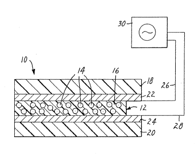
particular to FIG. 1, a variable grey-scale PDLC
device 10 according to the invention is shown. In
one embodiment, the device lo comprises a PDLC film
12 having a multiplicity of liquid crystal droplets
14 dispersed in a polymeric matrix 16.
Liquid crystal materials useful in forming
the droplets 14 are functionally nematic and suitably
birefringent. Typically they have at least one
nematic mesophase and display positive dielectric
anisotropy and/or positive diamagnetic anisotropy in
the polymer matrix 16. By "functionally nematic" it
is meant that the liquid crystal material is
conventionally considered to be "nematic" (e.g.,
birefringent nematic type, birefringent chiral
nematic type, as well as mixtures thereof) or, if not
considered "nematic" in the conventional sense, has
the capacity to function as a nematic material (e.g,,
cholesteric types and mixtures thereof).
Whether a liquid crystal material is
"suitably birefringent" may be determined with
reference to its optical anisotropy (~n). Liquid ,
crystal materials useful in,the invention are
biaxially birefringent and have essentially rod- -
æhaped molecules. The major axis of a liquid crystal
molecule is regarded as its optic axis. A body of
liquid crystal molecules in the nematic mesophase
displays an ordinary index of refraction (nO)
perpendicular to the optic axes of the molecules and
an extraordinary index of refraction (ne) parallel to
~0 the optic axes. The difference between the values of
ne and nO (the optical anisotropy or An) describes the
birefringence of the liquid c.ys~al ~aterial.
Typically preferred values for Qn for liquid crystal
materials useful in the invention are in the range of
,, . ~ . : .. ~ .. . . ... .
WO92/12219 PCT/US92/001
2~826 20
O.Ol to 0.5. Furthermore, nO should be closely
matched to the index of refraction of the polymer
matrix material (e.g., + 0.02, preferably, ~0.~2) so
as to enhance the transparency of the PDLC device in
the on-state. The polymer matrix material should be
optically isotropic so as to minimize undesirable
birefringence effects of the liquid crystal material.
Commercially available liquid crystal
materials useful in the invention include LICRISTAL
E7, BL006, BL009, ML1005, ML1008, 17151, 17153,
17315, 17722 (sometimes available under the trade
designation BL038) and 17723 (sometimes available
under the trade designation BL036) (all available
from EM Industries, Hawthorne, New York). Mixtures
of these liquid crystal materials may also be used.
Polymeric matrix materials 16 in which the
liquid crystal droplets may be dispersed preferably
comprise reaction products of materials such as
monomers, oligomers or reactive polymers which may be
polymerized by photoinitiation. Several
photoinitiation systems involving different
chemistries are known and may be used in the
invention to cure the uncured matrix material.
Suitable techniques for providing polymer
matrix 16 include radical polymerization of
monofunctional and/or multifunctional alkyl acrylates
and methacrylates. Useful monofunctional acrylate
monomers include, for example, unsaturated acrylate
esters of non-tertiary alkyl alcohols, the molecules
of which have from l to about 14 carbon atoms.
Included within this class of monomers are, for
sxample, iso3~til acrïlate, isononyl acrylate,
2-ethyl-hexyl acrylate, decyl acrylate, dodecyl
acrylate, n-butyl acrylate, and hexyl acrylate. The
- . ~
..: . ~ ,
,
,
W,~ 92/12219 PCI/US92/00173
` G
alkyl acrylate monomers may be used to form
homopolymers, copolymers or higher order polymers for
the polymer matrix material or they may be
copolymerized with polar monomers.
The polar copolymerizable monomers may be
selected from monomers such as acrylic acid, itaconic
acid, hydroxyalkyl acrylates, cyanoalXyl acrylates,
acrylamides or substituted acrylamides, N-vinyl
pyrrolidone, N-vinyl caprolactam, acrylonitrile,
~0 vinyl chloride or diallyl phthalate.
Non-polar monomers such as isobornyl
acrylate, dicyclopentadiene acrylate, etc. are also
suitable for use in the invention.
Multifunctional acrylates include 1,6
hexanadioldiacrylate, trimethylpropane triacrylate,
propylene glycol dimethacrylate etc. can be used as
major components of the matrix or alternatively may
be incorporated at lower levels ~e.g. 0.05 tG 2 parts
by weight of the total monomer content) to function
as crosslinkers.
Also useful in the invention are reactive
oligomers, such as allyl or (meth)acrylated oligomers
of polyurethanes, polyesters, polyols, polybutadienes
or epoxies. An example of a suitable acrylated
polybutadiene is SARTOMER CD 5000 (commercially
available from Sartomer Co.). A useful acrylated -
polyester is SARTOMER 609 (from Sartomer Co.) and a
suitable acrylated polyurethane is SARTOMER 9610
(Sartomer Co.).
Blends of the reactive oligomers and the
alkyl ester monomers described above may be used.
Blends may be useful n sdjusting certain 2ropert es
such as the refractive index of the polymer matrix
materlal, the solubility of the liquid crystal
', ' ' . ', ', ' ' ~ '1. ' ;1, ' ~ ., . '
.
~; ,. ~,
WO92/l2219 PCT/US92/0017~ ~~
2~96826
- 22
material in the polymer matrix material, or the
viscosity of the liquid crystal/polymer matrix
system. The ratio of oligomer to monomer will depend
on the physical properties of the oligomer and may
vary from neat monomer to neat oligomer. At the
temperature at which the mixture is to be applied to
a substrate (if a substrate is employed) (typically a
temperature in the range from about 60 to 120F
(about 16 to 49C)), the mixture should have a
viscosity which renders it coatable and the liquid
crystal material should remain soluble therein.
Where photopolymerization is desirable, the
polymer matrix material may also contain a
photoinitiator to aid in polymerization of the
monomers. Photoinitiators that are useful for
polymerizing the acrylate monomer include the benzoin
ethers, substituted benzoin ethers such as benzoin
methyl ether or benzoin isopropyl ether, substituted
acetophenones such as 2,2-diethoxy-acetophenone, and
2,2-dimethoxy-2-phenyl-acetophenone, substituted
alpha-ketols such as 2-methyl-2-hydroxypropiophenone,
aromatic sulphonyl chlorides such as 2-naphthalene
sulphonyl chloride, and photoactive oximes such as
l-phenyl-l,l-propanedione-2-(O-ethoxycarbonyl) oxime.
Generally, the amount of photoinitator is from about
0.01 part to about lO parts per lOO parts monomer
weight.
Other radical polymerization initiating
systems which may be used include 3,4-bistrichloro-
methyl-6-substituted-s-triazines, and benzophenone
with an amine, for example, benzophenone and
p-(N,N-diethylamino) ethyl kenzol.a~c.
Reactants useful for the polymeric matrix
material also include W polymerizable systems based
. , , . ~ . ,
. . ,
-,
Wf~92/12~19 PCT/US92/00173
~. ~
23 i2~
on thiol-ene chemistry. An,example of such a system
is based on the reaction products of triallyl
isocyanurate and/or other suitable mono-, di- and ~'
triallyl ethers or esters, and one or more suitable
5polythiol oligomers selected from the group
consisting of Z~OCO (CH2)nSH]m, wherein
Z = a polyvalent organic moiety which is a -
CHo_3 group-containing nucleus of a tri- or
tetravalent alcohol such as glycerol,
10trimethylolpropane or pentaerythritol;
m = 3 or 4; and
n = 1 to 5.
Other useful W polymerizable systems based ' '
on thiol-ene chemistry comprise, in major part,
15monofunctional or multifunctional allyl compounds
containin~ an hydroxyl group reacted with a mono- or
multifunctional isocyanate, which reaction product is
subsequently reacted with one or more sui~able
polythiol oligomers having the structure described
20above. This W polymerizable system may include
other allyl functional monomers. For example, the '~
system may optionally include as a third material, a ,
mono-, di-, or triallyl compound which reacts with
the polythiol.
The polymer matrix material may also
comprise a blend of monofun,ctional (meth)acrylates, ~'~
and/or multifunctional (meth)acrylates, and the
polythiol oligomers described above.
The proportions of the various allyl and/or
30(meth)acrylate compounds noted above in the several
different systems and the polythiol are selected so
as to p~c u~_ z relat~ Ply high m~lecular weight
polymer. Preferably the stoichiometric ratio of
allyl and/or (meth)acrylate compound to polythiol, is
: ~
- - . .
WO92/~2219 PCT/US92/001 ~ ,
2~682~ 24
in the range of about 1.5 to 2.5, more preferably,
about 2.
Examples of useful polymer matrices based
on thiol-ene chemistry include NOA 65 and NOA 68
(each commercially available from Norland Products,
Inc. New Brunswick, New Jersey) which include
photoinitiators.
The liquid crystal material may also be
dispersed in a polymer matrix formed by the
polymerization of a functional epoxy monomer or
oligomer, and a polyol. These systems can be
photoinitiated by diaryl iodium or triaryl sulfonium
salts such as triphenyl sulfonium
hexafluoroantimonate. Alternatively, photoactive
organometallic compounds known to catalyze epoxy
polymerization may be used,.such as those disclosed
in European patent publication no. 109,851.
Representative epoxy substituted compounds
which are useful as matrix precursors are discussed
in U.V Curing: Science and Technology (S. P.
Pappas, editor), published by Technology Marketing
Corporation, 1978, p. 45, which page is hereby
incorporated by reference. A suitable epoxy resin
mixture is, for example, a blend of EPON 828
(commercially available from Shell Chemical Co.) and
trimethylene glycol, in a ratio of about 4:1 parts by
weight and about 0.5 part (based on total epoxy
content) of an W energy activated curative such as
FC-508 (commercially available from Minnesota Mining
and Manufacturing Co.).
Various other monomers may be incorporated
into the polymer ma'erials described hereina~Gv~ '~
usefully adjust the physical characteristics thereof.
For example, other monomers may be included to adjust
.
WO92/12219 PCT~US92/00173
.
2096-~2~
the refractive in~ex of the polymer matrix material
relative to the refractive index of the liquid
crystal material.
The polymer matrix material should be
selected such that the liquid crystal material is
soluble in the photopolymerizable mixture, although
an application of heat may be necessary to achieve
this. upon polymerization of th~ mixture, the liquid
crystal material should become insoluble in the
polymer matrix and form droplets.
Formation of a PDLC film according to the
invention is typically carried out in a phase
separation process. Polymerization induced-phase
separation has been found to be useful when the
uncured polymer matrix material is miscible with a
low molecular weight liquid crystal material. Liquid
crystal droplets form when the solubility of the
liquid crystal material in the polvmer matrix
material decreases as a result of an increase in the
molecular weight of the matrix material which occurs
when the matrix material poly~èrizes to form a
continuous phase. As the solubility of the liquid
crystal material decreases, it phase separates from
the polymer matrix material and forms droplets. The
droplets increase in size until the polymer matrix
material locks in the final droplet morphology. The
liquid crystal droplets should be present in a range
of sizes (diameters) extending from about 0.1 to
about 10 microns (~), preferably about 0.8 to 5 ~,
and more preferably about 1 to 3 ~. The
polymerization is carried out in the presence of the
liguid c-ystal mat2rial there~y e.,a~ling tailoring of
the polymer matrix material in terms of molecular
weight, crosslink density, liquid crystal
~ , , ~ 1' :. : . . :
. . ~ : : . . -
. ~ . .. .
.
WOg2/12219 PCTtUS92/00173
209~82~ 26
compatibility, and adhesion.
Polymerization as described above involves
the phase separation of the liquid crystal material
from the polymer matrix material (upon curing or
polymerization of the matrix material). Therefore,
any premature phase separation should be prevented.
"Premature phase separation" refers to an unwanted,
thermally-induced phase separation that occurs before
the "desired" phase separation (which results from a
I0 decrease in the solubility of the liquid crystal
materiai as explained above). Premature phase
separation can be reduced by heating the liquid
crystal and uncured polymer matrix materials to form
a homogeneous solution and further by continuing to
apply heat pri~r to and during curing. With the
appropriate selection of the liquid crystal and
polymer matrix materials, it is believed that control
of premature phase separation by temperature
regulation results in the production of PDLC devices
having larger numbers of smaller diameter liquid
crystal droplets than is otherwise achievable.
Phase separation of the liqiuid crystal
material upon polymerization of the uncured polymer
matrix material to form a dispersion of droplets in
the matrix material may be enhanced by the addition
of a filler such as finely divided silica having a
B.E.T. surface area of at least 10 m2/g (preferably
50 to 400 m2/g) to the polymerizable matrix material
prior to the addition of the liquid crystal material.
Fumed or precipitated silica of either the
hydrophobic or hydrophilic type may be used. It is
believed tha 'he p.2sence of the silica changes the
solubility of the liquid crystal material in the
uncured polymer matrix material thereby desirably
.. ... ... . .. . .. . .. . ..
WO92/~2219 PCT/US92/00173
, ,~,.. :,~
27 ~2~6~
altering the dynamics of phase separation. ~he
amount of silica will vary depending on the
particular liquid crystal and polymer matrix
materials. Generally about 0.1 to 5 (preferably 0.5
to 2) weight percent silica based on the weight of
the polymer matrix material is effective. An example
of a commercially available hydrophobic fumed silica
which is useful in the invention is AEROSIL R 972
(available from Degussa corp.). An example of a
commercially available hydrophilic fumed silica is
CAB-O-SIL M-5 (~vailable from Cabot corp., Cab-O-Sil
Division, Tuscola, Il.).
Although an application of heat is useful
in preventing premature phase separation, heating the
system too much may adversely affect the phase
separation which should occur upon curing of the
polymer matrix material and may result in the
inability to create well-~ormed liquid crystal
droplets. The appropriate temperature range is a
function of the liquid crystal and polymer matrix
materials.
Preferably, the liquid crystal material and
the polymer matrix material are provided in
approximately equal parts by weight although the
2S parts by weight ratio of the liquid crystal material
to the polymer matrix material can vary from 40:60 to
60:40. If the liquid crystal material comprises less
than about 40 parts by weight or more than about 60
parts by weight, then one or more of the following
may be materially adversely.affected: switching
performance, adhesion, environmental stability and
cost.
Referring again to FIG. 1, although the
PDLC film 12 may be provided in free-standing form,
: . ~ . . . :
,. ~ . ~ . ......... : : : . , ,: , . : .
.
. . . . . . . ..
WO92/1221~ PCT/US92/00173
20~82~ ~
- 28
in many applications it will be desirable to provide
a sandwichlike construction in which the PDLC film 12
is interposed between a pair of first and second
substrates 18 and 20, respectively. It will be
understood that the device ~0 may be provided with
only a single substrate if, for example, the device
is to be applied to a motor vehicle sunroof or an
architectural window in which case the sunroof or the
window have a function analogous to that of the
second substrate.
Preferably, at least one of the substrates
18 and 20 is at least partially transparent to allow
incident visible light to pass therethrough. One of
the substrates (preferably the one on which light
first impinges) may be modified to have selective
light transmission characteristics, for example, to
selectively transmit light of a wavelength
corresponding to a cèrtain color o~ the visible
spectrum, ultraviolet light or infrared light.
Materials suitable for the substrates 18 and 20
include glass (which may be tempered) and plastics
such as polyester (or a copolyester),
polyethersulfone, polyimide, polyethylene
terephthalate, polyethylene naphthalate, poly(methyl
methacrylate), and polycarbonate. The substrates may
be treated so as to enhance their abrasion and
scratch resistance. The substrates are typically
about 25 to 50 ~ thick for flexible, durable
constructions, although they may range in thickness
from l ~ to greater than 250 ~O If glass is employed
for at least one of the substrates, a thickness in
excess of 250 ~ may be usaf-a'.
With continued reference to FIG. l, in
order to induce a change in the orientation of the
WO92/12219 ~ O 9 6 8 ~ ~ PCT/U592/0~173 ~ ~
29
liquid crystal droplets so as to cause the PDLC film
12 to switch between the translucent off-state and
the transparent on-state, it is necessary to apply an ~-
electric field across the film 12. (The PDLC film 12 ;
may also be switched by applying a magnetic field or
a thermal stress across the same.) Accordingly, the
device 10 may further comprise first and second
electrodes 22 and 24, respectively, which are
positioned intermediate the substrates 18 and 20 and
the PDLC film 12. The electrodes 22 and 24 are
connected to, respectively, first and second leads 26
and 28 (for example, a conductive adhesive tape or
the like) which, in turn, are electrically connected
to a variable power supply 30, preferably of the
alternating current type~ Preferably, the frequency
of the alternating field should be in the range of 40
to 100 hertz. The field should alternate
sufficiently rapidly so that a human observer of the
device cannot perceive flickering. Thus, upon
application of an electric field across the PDLC film
12, the optic axes of the liquid crystal droplets
become aligned. If the refractive indices of the
liquid crystal material and the polymer matrix
material have been closely matched, the film 12 will
switch between the translucent off-state and the
transparent on-state.
The electrodes 22 and 24 may be formed of
various materials including chromium, indium oxide,
tin oxide, stainless steel, indium tin oxide, gold,
silver, copper, aluminum, titanium, cadmium stanate,
other transition metal oxides, and mixtures and
allo~_ the-ecf. .~1ith the use cf C2, tain electrode
materials (e.g. silver) it may be desirable to
environmentally protect the same with a thin,
:. :. . ............ : , ., . - .
. - ~ . ~ . . : . :
WO92~12219 PCT/US92/0017~
20g682G
passivating dielectric layer. The use of such a
protective layer may enhance the ability of the
electrode to resist thermal, chemical, moisture
and/or ultraviolet-induced degradation. An example
of such a protective layer is Al2O3. The electrodes
must be capable of receiving an electrical input ~rom
the leads 26 and 28 and transmitting the same so as
to apply an electric field across the film 12.
Preferably the electrodes 22 and 24 are positioned
adjacent to opposite sides or surfaces of the film 12
and extend over, across and parallel to the same.
At least one of the electrodes 22 and 24
preferably comprises a conductive coating that is at
least partially transparent to visible light,
although electrodes which provide preferential light
transmission characteristics, such as color tint or
ultraviolet or infrared filter, may be used. The
electrodes 22 and 24 need not be equally transparent.
At least one of the electrodes should provide a
visible light transmission of at least 1%, preferably
at least lO~, and more preferably at least 50%. The
electrode coating should have a conductivity greater
than O.OOl mhos per square. The electrode material
may be coated or otherwise applied to the first and -
2S second substrates 18 and 20.
Maximum light transmission through the
device is determined by selection of material used
for the electrode and the thickness of the coating.
Typically, maximum light transmission ranges from
about 30% to about 80%.
In operation, a user of the device lO
~2nipulat2s and selectively ad~usts ~he varlakie
power supply 30 to vary the magnitude of the electric
field applied across the film 12 until the device lO
W~ 2/12219 PC~/US92/00173
` 2~9~2~ !
31
transmits the desired amount of specular light, the ~-
amount which is desired being dependent on the
particular situation.
The thickness of the PDLC f ilm 12
influences at least in part its optical
characteristics. Preferably, the film has a
thickness in the range of about 5 to 25 ~, more
preferably in the range of about lO to 25 ~, and most
preferably in the range of about 15 to 21 ~. If the
film thickness exceeds about 25 ~, the initial
voltage at which the device lO begins to switch may
be too high for effective use in relatively low
voltage environments (for example, an automobile) or
the device may require increased amounts of power to
switch between the translucent off-state and the
transparent on-state. The maximum voltage required
to fully switch the film should be less than 120
volts tV), preferably less than lOO V, and most
preferably between about 40 to 60 V. (All voltages
referenced herein are reported as root mean square
(RMS) values.)
On the other hand, if the PDLC film
thickness is less than about lO ~, the device lO may
appear transparent even in the off-state (i.e.,
without any voltage being applied). This might be
desirable in applications where it is necessary to
adjust thé degree to which specular light is
transmitted through the device when the device is in
the off-state such as for jurisdictions having motor
vehicle or building codes with minimum visibility
standards. Devices in which the PDLC film thickness
is about 5 _o lO ~ may alsG be -uae~-ul in
constructions where one of the electrodes is fully
reflective and the PDLC film functions as an anti-
. , . : . . . , , : .. .
., . . .,:
. , : . ~ ,. . ~ ,.
W092/~22t9 2 ~ 9 6 ~ 2 ~ PCT/US92/oo17~
32
reflection layer that can be transitioned between thetranslucent and transparent states at a relatively
low applied voltage. An example of such a device is
a membrane switch bearing a reflective pad in a
contrasting color relative to the switch backgrou~d
and in which the pad repeatedly cycles between the
translucent and transparent states when touched so as
to change visibility in low light environments.
The desired thickness of the PDLC film is
also related to the difference between the ordinary
(nO) and extraordinary (ne) indices of refracti~n or
the liquid crystal material. If ~he difference is in
the range of about 0.22 to about 0.26, a PDLC film
thickness in the range of 1~ to 21 ~ is preferred.
If the index of refraction difference is less than
0.22, then the film may need to have a thickness
greater than 21 ~. Alternatively, if the index of
refraction difference is greater than 0.26r then the
film may be comprised of a thickness less than 15 ~.
(The relationships between the index of refraction
and the PDLC film thickness assume a constant droplet
structure.)
Whether a particular device exhibits a
variable grey scale within the scope of the invention
may be determined with reference to a graphical plot
of the percentage of total light incident on the
device which is transmitted unscattered therethrough
(i.e., specular light) (referred to herein at times
as "~ transmission" or "~T") as a function of the
voltage which is applied across the PDLC film. More
particularly, whether a device exhibits a variable
grey ~cal2 m~i' be d2t2rmined ~-ith reference to the
voltage differential required to change the
transmissivity of the device from a first value to a
,: . :, , : :
.. ,. , , . , . ~ . :
. ' : ', . :, ., ,. - : ,
.
,
.. . : ~ : : .
WO92/12219 PCT/US92/00173
.,
2Q9682~
33
second value~
Whether a PDLC device exhibits a variable
grey scale is determined as follows;
The % transmission of the device is
s measured at o applied volts (referred to herein at
times as 1'%To") and lO0 applied volts (referred to
herein at times as "%Tloo"). The % transmission at
lOO V was selected for measurement since, for many
devices, a graphical plot of ~T vs. applied voltage
lO shows a slope of about O at that portion of the plot.
For those devices in which the %T has not reached a
plateau (i.e., the slope is not zero), lOO V provides
a convenient reference point. The difference
between %Tloo and %To is calculated, this difference
15 sometimes being referred herein to as "~%T" or "the
total change in % transmission" ("the total change in
%T"). 80% of ~%T and 20% of ~%T (sometimes referred
to herein as, respectively, "A%T80" and "AT~2C" are
then calculated. The %T at 0 applied volts (%To) is
20 then added to each of ~%T80 and ~%T20, the two sums
sometimes being referred to herein as, respectively,
a%T80+0 and ll~%T20+0 " The applied voltages
corresponding to ~%T80+0 and ~%T20+o are then
determined, these values sometime being referred to
25 herein as, respectively, V80+0 and V20+0. The voltage
differential between V80+0 and V20+0 (referred to
herein at times as ~V) is then calculated.
A variable grey scale is found when ~V is
greater than or equal to 15 V, more preferably
30 greater than or equal to 20 V, and most preferably in
the range of 20 to 30 V. ~evice performance may be
negatively mater ally affected if ~V is greater than
about 60 V.
In FIG. 2, a graphical plot of %T as a
-- - - . . ~ .- -
wos2/l~z1s PCT/US9~/00173~
~0~82~ 34 ~
function of applied voltage; the performance of a
PDLC device according to the invention is shown as
the curve labeled with the reference letter A. This
particular device has a %To of about 3% (i.e., a 3%
transmission at 0 applied volts corresponding to the
translucent off-state) and a %T1oo of about 97% (i.e,
a 97% transmission at 100 applied volts corresponding
to the transparent on-state). The ~T (%T1oo-%To) of
the "curve A" device is about 94% (i.e., 97% - 3%).
80% of ~%T (i.e, ~%T80) is 75.2% and 20% of ~%T (i.e,
~T20) is 18.8% thereby yielding a%T80+0 = 78.2%
(75-2% ~ 3%) and ~%T20+0 = 21.8% (18.8% + 3%). The ;
applied voltage corresponding to ~%T80+0 (i.e, 78.2~)
is 44 V (V80+0) and the applied voltage corresponding
to ~%T20~0 (i-e, 21-8%) is 22 v (V20+0). The
difference between the two applied voltages (i.e, aV)
is 22 V (44 V - 22 V).
The performance of a presently known device
is also illustrated in FIG. 2 as the curve labeled
with the reference letter B. (The data used to
prepare curves A and B in FIG. 2 were normalized so
that the performance of the two devices could be
fairly compared on the same graph. Data
normalization is a frequently used analytical
technique and is well understood by those skilled in
the art. In order to simplify the calculations
necessary to derive ~V, it is preferred that the data
be normalized to yield a maximum transmission (i.e, a
%T of 100%) at 100 V. In the preparation of FIG. 2,
however, the data were normalized to yield a maximum
transmission at 120 V. This did not alter the
validity o th~ data in~erpreta~ion -~in~e che
performances of both devices were normalized in the
same manner.)
.
WO92/12219 PCT/US92/00173
!
2~9~3~
The presently known device is manufactured
by and commercially available from Ajinomoto co.,
Inc., Tokyo Japan. using the sa~e method of
calculation as described above, the ~v of the
Ajinomoto device is about 8 volts. A ~V of less than
15 V is desired in applications where sharp switching
(such as for display arrangements or multiplexing) is
important. In these devices, it is desirable to
minimize both ~V and the threshold voltage (i.e, the
minimum applied voltage at which the device begins to
switch between the translucent and transparent
states). By minimizing both ~V and the threshold
voltage, the power needed to operate the device is
reduced because it begins to switcA at a lower
voltage and because it switches more sharply (i.e.,
it switches over a smaller voltage range or ~V). The
cost of the drive circuitry is al80 a major factor in
the overall performance of the display device. By
achieving a saturation voltage (i.e., the voltage
required to achieve a maximum % transmission) of 28 V
or less, the cost of the drive electronics
interfacing with the device can be significantly
reduced. A saturation voltage of 15 V or less is
preferred. Such considerations are important where
it is desirable to have sequential addressing of
certain areas (e.g., pixels in a display device).
In addition to a voltage differential of at
least 15 V, variable grey scale devices preferably
exhibit a uniform appearance as the voltage is varied
between the threshold voltage (corresponding to the
translucent off-state) and the maximum voltage
(~cr-esp^ndi~ ^ the t.ar.spa.ent on-state). That
is, the relative translucent/transparent appearance
should be substantially unifsrm across the entire
: . ' ,' ~. '~' . .
WO92/12219 PCT/US92/0017~ 1
2~9~26
36
PDLC device. A PDLC device according to the
invention will display a uniform appearance if it has
a ~V of at least 15 V. In those PDLC devices which
are presently known and which do not display a
variable grey scale, the transition between the
translucent and transparent states is uneven and
non-uniform. These devices tend to have a blotchy
appearance while transitioning.
As explained more fully below, it is
believed that the ability to achieve a variable grey
srale device having a uniform appearance during
transition is also related to the structure of the
liquid crystal droplets. That is, a range or
variation in the size or diameter of the liquid
lS crystal droplets positively contributes to the
provision of a PDLC device which uniformly
transitions between the translucent and transparent
conditions. Other characteristics o PDL~ devices
are also related to the attainment of a device which
has a uniform translucent/transparent appearance.
~or example, the PLDC device comprising liquid
crystal droplets dispersed in a polymer matrix
material should be of substantially equal thickness.
While this condition is necessary to achieving a
uniform appearance, it is not sufficient. Presently
known devices contain mechanical spacers to maintain
constant PDLC film thickness but tend to exhibit a
blotchy appearance while transitioning between the
translucent and transparent states.
Turning now to FIG. 3, there is shown a
schematic illustration of one method for producing
PDLC dev~ces accord,ng to the invention. Ir. order to
simplify understanding of the invention, it is -
assumed that the first and second substrates 18 and
:: , .
. ' . ~
WO92/12219 PCT/US92/00173
2~682~
37
20 are formed of the same material although it will
be understood that the substrates may be different.
As an example, a large (e.g., 60 inch (152 cm) width)
roll 32 of a suitable, flexible substrate material is
provided and has applied thereto an at least
partially transparent conductive electr~de to provide
a roll 34 of electrode-coated substrate. ~he
conductive electrode may be any of the materials
described hereinabove and may be applied to the
substrate roll 32 by chemical vapor deposition,
vacuum metalization, sputter coating or other similar
techniques as are well known in the industry, the
application step being identified generally by the
reference numeral 36.
Separate rolls 34 of electrode-coated
substrate are mounted on upper and lower rotatable
spindles 38 and 40. In production, the separate
rolls 34 correspond to, respectively, the first and
second substrates 18 and 20. The first and second
substrates 18 and 20 with the first and second
electrodes 22 and 24 having been applied thereto as
described above are supplied to upper and lower nip
rollers 42 and 44 of a precision, two roll nip coater
to bring the electrode-coated surfaces of the
substrates into facing relationship. (Nip rollers
42 and 44 may be heated, if necessary, to prevent
premature phase separation of the liquid crystal and
polymer matrix materials.) A pump 46 feeds liquid
crystal/uncured polymer matrix material blend from a
reservoir 48 to the nip rollers 42 and 44 by way of
conduit 50. The gap between the nip rollers 42 and
44 is adjusted so as 'o provide thz dzsirzd ~DLC ,i~m
thickness. After exiting from the nip rollers, the
temperature of the sandwichlike construction
,
.
'
WO92~12219 PCT/US92/00173
..~.
239682~
38
comprising the first and second substrates with the
liquid crystal/unpolymerized matrix material
therebetween is maintained (to prevent premature
temperature-induced phase separation) until it is
passed between two opposed banks 52 and 54 of
fluorescent, low intensity W lamps in order to
polymerize the matrix material. ~Preferably a
continuous pull-through manufacturing process is
used.) W lamp bulbs with different spectral
responses are commercially available and may be used.
In general, the polymerization chemistry of matrix
material and the absorption characteristics of the
photoinitiator may influence bulb section. Once
polymerized, the PDLC device lO may be collected in a
rolled form 56 for ease of handling.
Advantageously and contrary to known
production approaches for making PDLC devices
generally, the method described abo~e for
manufacturing PDLC devices employs relatively low
intensity W radiation sources having a continuous
emission spectrum, where a major portion of the
energy output of the source preferably falls within
at least a part of the wavelength range of 280 to 450
nanometers (nm). An example of such an ultraviolet
radiation source is a fluorescent lamp. Fluorescent
lamps are generally understood to have two kinds of
spectral power emission. One kind is a continuous
spectrum provided by the fluorescent phosphor. The
second kind comprises narrow bands of energy emitted
by the mercury component of the lamp. Thus, a
"continuous emission spectrum" is distinguished from
the na--ow band o_ 'in~ spectra a.forded by other
radiation sources such as high pressure mercury
discharge lamps. (Known PDLC production techniques
, ' :' ' . ' ~ . ' . :
, ' '' ,'' ~ ', j ' . ' .
WO92/12219 PCT/US92/00173
.. . .
2~9~2`~
39
utilize relatively high intensity W radiation
sources such as mercury or mercury/xenon discharge
lamps.) Preferred low intensity fluorescent lamps
have an emission spectrum in the range of 280 to 450
nanometers (nm).
If the liquid crystal/polymerizable material
mixture includes a phctoinitiator, the emission
spectrum of the w radiation source is preferably
selected so as to match the absorption spectrum of
the photoinitiator, thereby maximizing absorption of
the UV radiation by the photoinitiator and
accelerating the curing reaction (i.e.,
polymerization of the uncured matrix material).
Each of fluorescent lamp banks 52 and 54
may comprise a single low intensity fluorescent lamp
or a plurality thereof arranged sequentially.
Although an arrangement invol~ing a pair of opposed
fluorescent lamp banks ~such as illustrated in FIG.
3) is preferred, the lamps may be oriented to
irradiate only one side of the substrate and liquid
crystal/uncured polymer matrix material sandwich
construction.
Alternatively, higher intensity W
radiation sources which have been appropriately
filtered to provide low intensity radiation may be
used.
Preferably the average radiation intensity
of each of the fluorescent lamp banks is in the range
of about 0.25 to lO mW/cm2 (more preferably in the
range of about 0.5 to 5 mW/cm2). Furthermore, it is
preferred that the total radiation received by the
sandwich construction be in the range Gf abo-u. lûO ~0
1500 mJ/cm2 (50 to 750 mJ/cm2 per side). The
particular radiation intensity and total energy
,. .- . :
::
W092/1~219 PCT/US9~/~017~ 1 ~
2~9~82~ 40
exposure requirements will vary depending on the
liquid crystal, initiator a~d polymer matrix
materials~ '
It is believed th~t after only a relatively
short exposure (for example about lO seconds) to a
low intensity W radiation ~ource, the polymerizable
material which provides the polymer matrix 1 -
sufficiently gels to "lock in" the final liquid
crystal droplet morphology. It is b~lieved that
once the uncured matrix material has received about
30 mJ/cm2 of W radiation per side (for example a 30
second exposure to radiation having an intensity of
about l mW/cm2 per side~, the polymer matrix material
will have sufficiently gelled or set to allow for the
use of higher intensity W radiation.
For example, a "two stage low intensity" W
radiation approach may be used in which a "first
stage" having a radiation intensit-y of less than or
about 3 mW/cm2 is followed by a "second stage'~ having
a radiation intensity of less than about lO mW/cm2
but greater than that used in the "first stage," both
sides of the construction typically being exposed in
each stage. Alternatively, after an initial W
radiation intensity exposure of less than or about 3
mW/cm2, the rate of polymerization or curing of the
matrix material may be accelerated by exposing one
side of the partially cured (i.e., partially phase
separated) system to "high intensity" W radiation,
for example, radiation having an average intensity of
about 20 to 200 mW/cm2 (total energy exposure in the
"high intensity" stage of about 200 to 1500 mJ/cm2).
The actual rad atio. intensity and exposure
requirements will vary with the liquid crystal and
polymer matrix materials.
. ~ : : - :
W~92/12219 PCT/US92/00173
',':`.
41 2~6826
The use of low intensity w radiation
sources, as opposed to higher intensity Uv sources,
offers several advantages. For example, low
intensity fluorescent lamps (unlike the presently
used high intensity, medium or high pressure mercury
and mercUry/Xenon radiation sources) operate at lower
temperatures thereby reducing or eliminating the need
for elaborate and expensive cooling systems.
Infrared heating of the sample is minimal; elaborate
light filters are not needed to control cure
parameters. Also, low intensity fluorescent lamps
can be immediately restarted following a production
shut-down (unlike the mercury and mercury/xenon
sources).
As noted hereinabove, it may be desirable
in certain applications to provide a PDLC device
comprising a film which is bonded to only one
substrate or comprising a free-standing film. In the
case of a PDLC device having only a single substrate,
the process described above is employed except that
the substrate supplied from the lower spindle 40 to
the lower nip roller 44 is a 25 ~ polyester film
which has not had electrode material applied thereto.
once the uncured polymeric matrix material has been
polymerized upon exposure to W radiation, the
untreated polyester film is peeled away. In the case
of a free-standing PDLC film, neither substrate in
the above described process is provided with
electrode material. After the matrix material has
polymerized upon exposure to W radiation, both
substrates are removed.
Whether the PDLC devic~ i~ supplied as a
free-standing film, with one substrate, or with two
substrates, the device may be applied to a surface
.. .
..
, . . .
,
WO92/12219 PCT/US92/00173~?
2~9682~ !
42
such as a motor vehicle sunroof, a motor vehicle side
window, or an architectural window with, for example,
a suitable adhesive. (Preferably, the adhesive is
optically transparent.) As noted hereinabove, by
varying the magnitude of the electric field with the
variable power supply 30, a user of the variable grey
scale PDLC device lO can selectively adjust the
amount of specular light transmitted therethrough.
The device lO can be adjusted to have 0% relative
transmission, 100% relative transmission, or an
infinite number of intermediate specular light
transmission levels. As the device transitions
between the translucent off-state and the transparent
on-state, the device preferably has a uniform, even
appearance.
It should also be emphasized that the above
described process provides unique advantages over
those production methods which are presently known.
Whereas other PDLC devices require the use of pre-
sized mechanical spacers (poly(methyl methacrylate)balls, silica particles, and the like) to maintain
constant spacing between the substrates and the
electrodes and hence a substantially equal PDLC film
thickness, the present invention requires no spacers.
Spacing between the substrates is controlled by
mechanically adjusting the gap between the nip
rollers. The elimination of mechanical spacers and
the use of a precision two roll nip coater allows for
the production of thin, flexible, conformable PDLC
devices having thin substrates. Most examples in the
reference literature discuss the use of glass
substrates and the presently known, commercially
available structures include 7 mil (178 ~) substrates
which provide limited flexibility and virtually no
WO92/12219 PCT/US92/00173
;; ~
~9~2~ `
43
conformability.
The invention will be more fully understood
with reference to the following examples which are
not to be construed as limiting the scope of the
invention.
Gener~l Preparation of a PDLC Device
A PDLC device was formed as described
below. Equal parts by weight of LICRISTAL E7 liquid
crystal material and NOA65 polymer matrix material
were combined with heating and stirring until the
liquid crystal material completely dissolved. The
liquid crystal/uncured polymer matrix material blend
was poured between a pair of 25 ~ thick polyester
films which pre~iously had been coated with a silver
electrode material on one surface of each film. The
two films were held with their electrode-coated
surfaces in facing relationship by the nip rollers of
a precision two roll nip coater. The gap between the
nip rollers was set to provide a liquid crystal
material/uncured polymer matrix material film
thickness of 15 to 18 ~.
The uncured polymer matrix material was
polymerized by positioning the sandwichlike
construction comprising the two electrode-coated
substrates and the liquid crystal
material/unpolymerized matrix material between a pair
of opposed banks of fluorescent black light phosphor
lighting elements, each bank being positioned to
illuminate one of the polyester films. Lighting
elements having a spectral ~istribution between 300
to 400 nm and a maximum output a'~ 3~. nm were
employed.
The lighting elements were adjusted so as
- .
- ~
.
WO92/12219 ~ PCT/US92/0017~ 1
2a9~82~ ~
44
to provide an average intensity of l to 2 mW/cm2
through each electrode-coated polyester film (i.e.,
per side). Each side of th~ sandwichlike
construction received a total energy axposure of 100
millijoules/sq. cm (mJ/cm2). The construction as a
whole was exposed to a total energy of 200 mJ/cm2.
The level of incident radiation was determined with
an EIT low intensity WIMAP radiometer or WIRAD
radiometer each having a spectral response in the
range of 300 to 400 nm and a maximum response at 358
nm.
Electrically conductive adhesive tape was
secured to a portion of each electrode-coated
substrate that had not had liquid crystal/uncured
matrix material applied thereto. Each tape was then
connected to an alternating current (AC) power supply
having a variable voltage output.
Ex~mples l-lO
A series of PDLC ~evices was prepared as
described above in the general preparation except
that the particular liquid crystal material employed
was varied as shown below in Table l.` In examples l
and 2, the average intensity of the W radiation was
l.l mW/cm2 per side. In examples 3 to 7, the average
intensity of the W radiation was 2 mW/cm2 per side
and the total energv to which the entire structure
was exposed was 300 mJ/cm2 (150 mJ/cm2 per side). In
examples 8 to lO, the average intensity was 2 mW/cm2
per side and the total energy was 200 mJ/cm2 (lO0
~J/cm2 pe. side,. T,~a op~ical performance of each
PDLC device was evaluated by measuring the applied
voltage necessary to provide various levels of
i. : ,, . ~
. .: . - . .
WO92/~2219 PCT~US92/00173
2~826
specular light transmission through the device and
graphically plotting the data to provide a ~T v.
applied voltage curve as described above. The curve
labeled with the reference letter A in FI~. 2 is
based on an evaluation of the PDLC device of example
2.
More specifically, specular transmission
(%T) for a particular applied voltage was measured
with a Perkin-Elmer LAMBDA g spectr~photometer having
an integrating sphere. Measurements were made at a
wavelength of 550 nm. The acceptance angle of the
optical system was between 3 and 4. PDLC samples
were switched with a VARIAC variable AC power supply
operating at a frequency of 60 hz. '
Table 1 reports values for ~V, as described
more fully hereinabove.
T~ble 1
. ._ _ . . . .
¦ Example No. E7 V
l .
¦ 2 BL009 23
¦ 3 ML1005 40
4 _ 17151 = S
6 17153 43
7 17315 30
8 BL0 0 6 21
1 v~ __ 17723 2
.. . .. . . . . .
:. :
.-
. . :. . . .. . .
. . . :::; ,. :
. . . ~
WO92/12219 PCT/US92/~0173
2~6~25 ~
46
lThe liquid ~rystal materials are
identified by their commercial trade
designation. All liquid crystal materials
are commercially available from EM
Industries, Hawthorne, NY.
Table l shows that a wide variety of liquid
crystal materials may be employed in PDLC devices
according to the invention. The switching curve for
each example had a av of at least 21 V and exhibited
a uniform visual appearance upon transitioning
between the translucent off-state and the transparent
on-state. -
With reference to FIG. 4, a photomicrograph
(enlarged 3000X) of the PDLC device of example 2, the
liquid crystal droplets range in size from about 0.1
~ to about 3 ~. The range of droplet sizes allows,
at least in part, for the PDLC device to gradually,
smoothly and uniformly transition from the
translucent off-state, through an infinite number of
intermediate states, to the transparent on-state.
Droplets of dif~erent size require different applied
voltages in order to switch. Some of the droplets
exhibit a nonuniform shape.
FIG. 4 also shows that liquid crystal
droplets clustered near opposed, major planar
surfaces of the PDLC film tend to be smaller in size
than droplets clustered in a zone intermediate areas
adjacent to the major planar surfaces.
~SX~pl~ 11 .,.
A PDLC device was prepared as described
above in the general preparation except that the
li~uid crystal ~aterial was BL003, the polymer matrix
material was NOA68, the W radiation average
intensity was 2 mW/cm2 per side, and the total energy
- . . . . . . . . .
.~ , . . . .
W092/12219 PCT/US92J0~173
F ~, ¦
47 2~96~2~ f
to which the construction was exposed was 300 mJ/cm2 f'
(150 mJ/cm2 per side). The optical performance of
the device was evaluated as described above. In a
graph of %T v. applied voltage, the device of example
ll had a ~V of 30 V and displayed a uniform visual
appearance upon transitioning between the translucent
off~state and the transparent on-state.
~xamples 12~
A series of PDLC devices was prepared as
described above in the general preparation to observe
the effect of varying the thickness of the
substrates. Substrate thickness and the liquid
crystal material were varied as shown below in Table
2. In examples 12 and 13 the W radiation average
intensity was l.92 mwtcm2 per side and the total
energy was l9l mJ/cm2 (95.5 mJ/cm2 per side). In
example 14 the W radiation average intensity was l.l
mW/cm2 per side and the total energy exposure was lO0
mJ/cm2 ~50 mJ/cm2 per side).
T~ble 2
. . ,
Example Liquid Substrate ~V
No. CrystalThickness
Materiall (~)
12 E7 51 22
Z5 13 BL009 51 22 1
, .. ,~ .. . 11
14 BL009 178 37
lThe liquid crystal materials are
identified by their commercial trade
designation. All liquid crystal materials are
commercially available from EM Industries,
~awthorne, NY.
In each example, the PDLC device had a ~V
greater than 20 V and exhibited a uniform visual
- -
.
'
WO92/12219 PCT/US92/00~73
~96~2~ ~ -
48
appearance upon transitioning between the translucent
off-state and the transparent on-state. The grey
scale performance of a PDLC device was not materially
affected by varying the substrate thickness.
~x~mpl~s 15-17
A series of PDLC devices was prepared as
described above in the general preparation with the
exception that the liquid crystal material was BL009.
The average intensity of th~e W radiation was l.1
mW/cm2 per side and the total energy exposure was 100
mJ/cm2 (50 mJ/cm2 per side). The proportions of
liquid crystal material and polymer matrix material
were varied as shown below in Table 3. The liquid
crystal material and polymer matrix material amounts
are reported in parts by weight.
T~ble 3
_ . _............. . . ._~ _
Example No. Amount of Amount of ~V
Liquid Polymer
Crystal Matrix
_ Material Material
_ 40 60 20
16 50 50 17
.... ~ ... .. __ .:
17 60 _ 40 _ 29
Each example had a ~V of at least 15 V and
exhibited a uniform visual appearance upon
transitioning between the translucent off-state and
the transparent on-state. Increasing the proportion
of liquid crystal material decreased the percentage
of specular light transmitted through the device in
~0 the ^PP-st-' e -..d ,~duced th2 maxl~-um ~T.
: . ~ .
- - : ..
.
W092/12219 PCT/US92/00173
i. ...................................................... .
4~ ~96~
~ pl~ 18-l9
A series of PDLC devices was prepared as
described above in the general preparation except
that the liquid crystal material was BL009, the parts
by weight ratio of liquid crystal material to polymer
matrix material was 60:40, and the thickness of the
liquid crystal material/polymer matrix PDLC film was
varied as shown below in Table 4. The average
intensity of the W radiation was l.l mw/cm2 per side
and the total energy exposure was lOo mJ/cm2 (50
mJ/cm2 per side).
T~ble ~
...... _ . . _.
Example No. PDLC Film ~v
Thickness (~)
18 l9
l9 - lO 33
_ 17_ _ 18 1 29
Each device had a ~V of at least 15 V and
exhibited a uniform visual appearance upon
transitioning between the translucent off-state and
the transparent on-state. It was observed that
thinner films had an increased %T at 0 applied volts
(corresponding to the off-state condition) than did
thicker films.
~Ampi~ 20
A PDLC device was prepared as described
above in the general preparation except that the
electrode material was indium tin oxid~ on a 178
thick polyester film. The average intensity of the
W radiation was l.l mW/cm2 per side and the total
~ . . . . . . .
:
.. . ... . .
- . - . . : : :
:- - . : . ~ , . , . :
. ~ . . . - . ,. ,. :
W092/1~219 PCT/US9~10017~ !
~6g26 .,.
energy exposure was lO~ mJ/cm2 (50 ~J~cm2 per side).
The device had a ~V of 37 V and demonstrated a
uniform visual appearance upon transitioning between
the translucent off-state and the transparent 1 -
on-state. Changing the electrode material did not
materially adversely affect the performance of the
device.
.
~s~mples 21-22
In example 21, a PDLC device was prepared
as described above in the general preparation except ,
that the LICRISTAL E7 liquid crystal material was
supplemented with 0.1% (by weight of the LICRISTAL
E7) of CBl5, a cholesteric liquid crystal material
comprising a cyanobiphenyl mixture having a 2-
methylbutyl alkyl group and commercially available
from EM Industries. The average intensity of the W
radiation was l.l mW/cm2 per side. The total energy
exposure was lO0 mJ/cm2 (50 mJ/cm2 per side). Example
22 paralleled example 21 except that the LICRISTAL E7
was replaced by BL009. The electrodes of examples 2l
and 22 included a thin, protective, passivating
dielectric layer. Each device had a ~V of 23 V and
demonstrated a uniform visual appearance upon
transitioning between the translucent off-state and
the transparent on-state. These examples show that
cholesteric liquid crystal materials may be used in
accordance with the invention.
Examples 23 to 27 below illustrate the
benefit of reducing or preventing premature,
ther~ally-induced phase separation by heating the nip
rollers and/or regula~in~ the air tempsrature in the
zone preceding and into the zone containing the low
intensity fluorescent lamps~ The particular air and
........ , . . ~ , ......................... ~ , --
. .
,, - .
: . : . . . - . .
W092/12219 PCT/US92/00173
~ a ~ S~ ~
51
nip roll temperatures are a function of the liquid
crystal and polymer matrix materials. In each
example, the temperatures were selected to allow for
the creation of well-formed liquid crystal droplets.
The thickness of each substrate in examples 23 to 27
was about 50 ~. The electrodes in each of examples
23 to 27 included a thin, protective, passivating
dielectric layer of Al203.
Exampl~ 23
A PDLC device was prepared according to the
general preparation except that the liquid crystal
material was 17723 (BL036) and the thickness of the
PLDC film was about 20 ~. Furthermore, the nip
rollers were maintained at about 85F (29C) and the
air temperature in the zone preceding and into the
zone containing the fluorescent lamps was maintained
at about 90F (32C). Each side of the sandwich
construction comprising the pair of electrode-coated
substrates and the liquid crystal material/uncured
polymer matrix material was first exposed to W
radiation of l mW/cm2 average intensity for about lO
seconds followed by a subsequent average intensity
exposure of 2 mW/cm2 for 2 minutes for a total
subsequent energy exposure of 480 mJ/cm2 (240 mJ/cm2
per side). The resulting PDLC device i~cluded a
multiplicity of liquid crystal droplets having sizes
ranging from about 0.6 to about 2.2 ~ dispersed in
the cured polymer matrix. The device exhibited a ~V
of 35 V and a uniform visual appearance upon
transitioning between the translucent off-state and
the transparent on-state.
WO92/12219 PCT/US92/0017~ ,
2 ~ . ~
52
~x~pl~ 24
A 20 ~ thick PDLC device was prepared
according to example 23 except that the temperature
of the nip rollers was a~out 92F (33C), the air
temperature in the zone preceding and into the zone ,
containing the fluorescent light banks was about 92F
(33~C), the initial average W radiation intensity
was 0.5 mW/cm2 per side (30 mJ/cm2 total energy
exposure, 15 mJ/cm2 per side), and the subsequent W
radiation exposure was provided by a 200 Watt/inch
high intensity mercury lamp with an average intensity
of 24 mW/cm2. (Total energy exposure was 1159 mJ/cm2
and the cure time was ~o seconds.) The liquid
crystal droplets in the resulting PDLC device ranged
in size from 1.1 to 3.2 ~. The device exhibited a ~V
of 26 V and a uniform visual appearance upon
transitioning between the translucent off-state and
the transparent on-state.
ExAmple 25
A 20 ~ thick PDLC device was prepared
according to example 23 except that the polymer
matrix material was blended with 0.5 % by weight
(based on the weight of the polymer matrix) of
AEROSIL R 972 hydrophobic fumed silica using a high
speed air mixer. The liquid crystal material was
then added and thoroughly mixed to provide a uniform
dispersion. The temperature of the nip rollers was
about 93F (34C) and the air temperature in the zone
preceding and into the zone containing the
fluorescent light banks was about 92F (33C). The
sandwich construction was cured for eight minutes
under a low intensity W radiation source that
provided an average intensity of 0.54 mW/cm2 per side
~:. . , . : - . .
:. . . , ,, ~
. .
WO92~l2219 PCTtUS92/00173
.?~
, ` .
53 2~ Q 6(~2~,
and a total energy exposure of 518 mJ/cm2 (259 mJ/cm2
per side). The liquid crystal droplets in the
resulting PDLC device ranged in size from 0.8 to 2.7
~. The PDLC device displayed a ~V of 35 V and a
uniform visual appearance upon transitioning between
the translucent off-state and the transparent ~n-
state.
~ ple 26
A 20 ~ thick PDLC device was prepared
according to the procedure of example 23 except that
the liquid crystal material was BLOo9. The
temperature of the nip rollers was about 110F (43OC)
and the air temperature in the zone preceding and
into the zone containing the fluorescent lamps was
about 120F (49C). (Higher temperatures were
required to prevent the premature temperature-induced
phase separation of the BL009 liquid crystal material
as compared to the BL036 liquid crystal material.)
The intensity of the initial W radiation exposure
was 0.72 mW/cm2 per side for 10 seconds (total energy
exposure = 14 ~J/cm2; 7 mJ/cm2 per side). The
subsequent W radiation exposure provided an
intensity of 2.4 mwtcm2 per side and a total energy
2~ of 288 mJ/cm2 per side. With reference to FIG. 5, a
photomicrograph (enlarged 2500X) of the PDLC device
of example 26, the resulting liquid crystal droplets
were well formed and ranged in size from 0.7 to 2 ~.
The PDLC device demonstrated a ~V of 33 V and a
uniform, visual appearance upon transitioning between
the translucent off-state and the transparent on-
state.
:
W092/12219 PCr/US92/~017~
2~9~2~ 54 ~ .
~x~ple 27
A PDLC device was prepared according to the
procedure of example 23 except that the liquid ;
crystal material was LICRISTAL E7 and the thickness
of the PDLC film was about 15 ~. The temperature of
the nip rollers was about 67F (19C) and the air
temperature in the zone preceding and into the zone
containing the fluorescent lamp banks was about 70F
(21C). The sandwich construction was exposed to low
intensity W radiation (average intensity = 1.7
mW/cm~ per side) for 2 minutes (total energy exposure
of 418 mJ/cm2, 209 mJ/cm2 per side). The liquid
crystal droplets ranged in size from 0.5 to 1.6 ~.
The resulting PDLC device had a av of 20 V and
exhibited a uniform visual appearance upon
transitioning between the translucent off-state and
the transparent on-state.
Reasonable variations or modifications are
possible within the scope of the foregoing
specification and drawings without departing from the
spirit of the invention which is defined in the
accompanying claims.
. . : . . - , : .: . . . .- ,
, , ,- . . . : ~ . . , : :
,~ . , . : ., : ,~ . ~ :
- . . . . .