Note: Descriptions are shown in the official language in which they were submitted.
~o ~sfia as
-1-
HIGH BANDWIDTH PACKET SWITCH
Technical Field
This invention relates to the field of packet-switched communications
networks, and, more specifically to packet-switching control data information
among
control units in a distributed processing switching system.
Background of the Invention
As more packetized data is being transmitted on the telephone network,
there is a need for increasing the speed (bandwidth) of the network. Modern
telecommunications networks can only be as fast as the packet switching
systems used
to route the data packets from source to destination. Therefore, there is a
need for
higher bandwidth packet switching systems.
Switching systems are relying more and more on distributed control to
increase the speed at which they can switch data packets and voice calls.
Distributed
control switching systems, which are conceptually small telecommunications
networks,
use packet switching for communicating control information rapidly among the
distributed processors. Without fast communication of control information, the
capacity of the switch becomes limited by the number of control messages that
can be
handled at one time, thus causing a bottleneck in the network. Therefore, both
the
network in general, and distributed processing switching systems specifically,
have a
need for high bandwidth packet switching.
Various packet switching systems have been tried for routing control
information in distributed processing switching systems with varying degrees
of
success. Some systems have provided a separate controller bus structure to be
used
for all communications among the processors. Other systems have utilized
dedicated
communication paths of the switching system to provide communication between
the
distributed system processors and a central controller which interprets
control
information and directs the overall operation of the switching system. These
known
systems, however, require that complex and time consuming operations be
performed
in their implementations. Such systems cannot take full advantage of
distributed
processing due to their reliance on a central controller to direct the
distributed
processors.
rj ,
-2- 209677
A control information communication arrangement in accordance with
the invention of U. S. Patent No. 4,322,843 of H. J. Beuscher et al., issued
March 30,
1982, achieves the benefits of interprocessor communication while reducing the
complexity and time consuming nature of previous arrangements. In accordance
with one exemplary embodiment of the invention of the Beuscher patent, control
units intercommunicate via certain switching system communication paths by
means
of control messages or packets comprising a plurality of control words. A
control
distribution unit included in the system accumulates the received control
words into
control packets and stores all such control packets in a shared memory. The
control
packets are then sequentially packet switched by transferring the packets
individually from shared memory to appropriate facilities for subsequent
transmission to destination control units defined by the packet headers.
However,
the sequential nature of the packet switching mechanism substantially limits
the
capacity of the control distribution unit to switch control packets. This
limitation
becomes particularly significant when the system control processors are used
to
implement features associated with the provision of integrated services
digital
network (ISDN) capabilities.
One potential solution to this problem is found in U. S. Patent
No. 4,821,259 of DeBruler et al., issued April 11, 1989, wherein a packet
switch for
inter-module communication within a switch is disclosed which packet switches
inter-module control packets via independent paths to high speed outgoing
packet
channels for transmission to destination control units. A ring-based packet
switch is
disclosed in one exemplary embodiment of the invention of the DeBruler patent,
with a circuit-switched fabric controlled in real time by a high speed,
multiple token
passing ring. However, this system is expensive to retrofit onto an existing
switching
system because packet channels and circuit channels have to be segregated when
the
link first enters the intermodule connection unit, and because modifications
must be
made to each module of the distributed processing switch that communicates
through this system, as well as each packet and circuit switching control
units.
Furthermore, each of these packet switches have buffering of the
incoming data packet at the input port. Such buffering requires at least the
duration
of receipt of a packet to accumulate a data packet before it is routed through
the
packet switch, thus taking time before the packet can be switched.
Furthermore,
moving an entire data packet through a switch is a tune-consuming process. In
some
examples, such as DeBruler, the data packet is again buffered at the output
port,
requiring more time. Therefore, buffering of packets before and/or after
switching
-3- zo9~g ~~
causes loss of performance in known packet switches.
In view of the foregoing, a recognized problem in the art is the limited
capacity of packet switching facilities used for interprocessor control
communication
in distributed processing switching systems.
Summary of the Invention
A low cost, fast packet switch according to this invention uses one buffer
directly connected between a plurality of input ports and a plurality of
output ports to
effect rapid throughput of data packets. Advantageously, a pointer to a
location in the
buffer is allocated by a buffer manager upon receipt of notification of an
incoming
packet at the receiving input port and the input port delivers the packet as
it is
received to the location designated by the pointer. After the data packet is
received,
the input port delivers the pointer and a destination address for the packet
to a router,
which selects one of the plurality of output ports based on the destination
address.
The router queues the pointer in a queue for the selected output port. The
output port
then retrieves the data packet from the buffer using the pointer to determine
the
location, and transmits the data packet. After the transmission is complete,
the output
port returns the pointer to the buffer manager. Advantageously, a packet
switch,
according to this invention, may be pipelined to receive, route, and transmit
simultaneously on adjacent ports.
A packet switch according to this invention may be implemented on one
board, thus facilitating easy retrofit onto existing distributed control
switching systems
with minimal modifications to other modules.
In accordance with one aspect of the present invention there is provided a
fast packet switch for routing data packets from a source to a destination,
said data
packets having a destination address, said switch comprising: a plurality of
input ports,
a plurality of output ports, a buffer connected to said input ports and said
output ports,
a buffer manager connected to said input ports and said output ports, and a
router
connected to said input ports and said output ports; said buffer manager
selecting a
location in said buffer in response to notification of receipt of a data
packet at one of
said input ports and producing data representing said buffer location, said
input ports
each having means responsive to receipt of said data representing said buffer
location
~x delivering said incoming packet to said buffer location; said muter having
means
-3a-
responsive to receipt of said data representing said buffer location and said
destination
address from said input ports for delivering said data representing said
buffer location
to a selected one of said plurality of output ports responsive to said
destination
address; each of said output ports having means responsive to receipt of said
data
representing said buffer location for retrieving said data packet from said
buffer
location, transmitting said data packet and returning said data representing
said buffer
location to said buffer manager.
In accordance with another aspect of the present invention there is
provided a method for use in a packet switch for routing data packets from a
source to
a destination, said data packets each having a destination address and an end
of packet
signal, said packet switch comprising an input port, a plurality of output
ports, a
buffer connected to said input port and said output port, a buffer manager for
allocating and deallocating pointers to locations in said buffer, and a router
means for
selecting one of said plurality of output ports, said method comprising:
responsive to
receipt of a data packet from said source, said input port requesting a
pointer from
said buffer manager; responsive to said pointer request, said buffer manager
allocating
a pointer corresponding to a specific buffer location; responsive to receipt
of said
pointer, said input port delivering said data packet to said buffer, starting
at said
location, as said data packet is received from said source; responsive to
receipt of said
end of packet signal, said input port delivering said pointer and said
destination
address to said muter means; responsive to receipt of said pointer and said
destination
address, said router selecting one of said plurality of output ports, and
delivering said
pointer to said selected output port; responsive to receipt of said pointer,
said selected
output port retrieving said data packet from said buffer and transmitting said
data
packet to said destination; and responsive to transmitting said end of packet
signal,
said selected output port returning said pointer to said buffer manager.
Brief Description of the Drawing-s
FIG. 1 is a block diagram illustrating an exemplary embodiment of this
invention in the context of a distributed control switching system;
FIG. 2 is a diagram illustrating a fast packet switch as shown in FIG. 1,
built according to an exemplary embodiment of this invention;
~'w
Q~~~ ~'~
-3b-
FIG. 3 is a more detailed block diagram of the time slot channel sequencer
of FIG. 2 according to the exemplary embodiment of this invention;
FIG. 4 is a timing diagram showing the timing of data through the fast
packet switch of FIG. 2;
FIG. 5 is a block diagram of the packet receiver of FIG. 2 according to
the exemplary embodiment of this invention;
FIG. 6 is a diagram of the layout of the protocol state registers of the
packet receiver of FIG. 5;
-4- 2096'77
FIG. 7 is a diagram of the layout of the address state registers of the
packet receiver of FIG. 5;
FIG. 8 is a diagram of the layout of the protocol state registers of the
packet transmitter of FIG. 10;
FIG. 9 is a diagram of the layout of the address state register of the
packet transmitter of FIG. 10;
FIG. 10 is a block diagram of the packet transmitter of FIG. 2 according
to the exemplary embodiment of this invention;
FIG. 11 is a block diagram of the router of FIG. 2 according to the
exemplary embodiment of this invention;
FIG. 12 is a block diagram of the buffer manager of FIG. 2 according to
the preferred embodiment of this invention;
FIG. 13 is a dining diagram at output of the buffer manager of FIG. 12;
and
FIG. 14 is a timing diagram at the input of the buffer manager of
FIG. 12.
Detailed Description
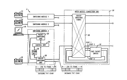
FIG. 1 is a block diagram illustrating an exemplary embodiment of this
invention in the context of a distributed processing switching system, wherein
a fast
packet switch 10 according to this invention is used to route packets
containing
control messages from a source module to a destination module. Switching
system 4
includes a plurality of switching modules, e.g., 1, 2, and 3, to provide both
circuit
switching and packet switching service, via a plurality of access ports, to a
plurality
of user stations, e.g., 12, 14, 16, and 18. In this exemplary embodiment, user
stations 12, 14, and 18 are telephone station sets, such as AT&T ISDN 7506 or
7507
telephones. User station 16 is a data terminal, as is known in the art. Each
user
station transmits information to and receives information from its associated
switch
module, for example switch module 3, in two circuit-switched B-channels and
one
packet-switched D-channel (which is a typical ISDN line). B-channels are
connected to a circuit switching unit 20 and D-channels are connected to a
packet
switching unit 22.
A control unit 24 is used both to control the establishment of circuit
switched connections by circuit switching unit 20 and the establishment of
packet
switched connections by packet switching unit 22. Communications interface 26
provides protocol handling for interprocessor communication.
-5- 2095877
Each switching module is connected to an inter-module connection
unit 28 by a 256 time slot, incoming time multiplex link and a 256 time slot,
outgoing time-multiplex link. Packet channels comprise one or more time slots
on
the ingoing/outgoing time multiplexed line. In FIG. 1, the 3 shaded time slots
shown
in the 256 time slot (TS) frame comprise a packet channel between switching
module 3 and the fast packet switch. Circuit switched paths are permanently
set up
at the time of initialization to provide a clear channel between the
communications
interface 26 and the fast packet switch 10. Note that the packet channels from
both
switch module 2 and 3 have circuit switched paths to the same port on the fast
packet
switch. In the exemplary implementation, each port on the Fast Packet Switch
is
capable of handling up to 32 packet channels. Packets received on the incoming
packet channels are switched in circuit switching fabric 30.
A telephone call is initiated from telephone 18 to telephone 12, for
example, by the user of telephone 18 removing the handset from the switchhook,
which causes telephone 18 to send a message to packet switch unit 22. In
response
to the message, packet switch unit 22 informs control unit 24 that telephone
18 has
gone offhook and control unit 24 causes circuit switching unit 20 to send a
dial tone
to telephone 18. The user of telephone 18 then enters digits which are sent
via
packet switching unit 22 to control unit 24. Control unit 24 performs digit
analysis
on the digits collected from telephone 18 and, as a result, decides that the
call is for
telephone 12, connected to switch module 1.
Control unit 24 formats a message for the control unit in switch
module 1 (not shown) to inform the switch module that it needs to request
switch
module 1 to determine if telephone 12 is busy. Control unit 24 formats a
message
and sends it through communications interface 26, which packages the message
in a
standardized protocol and sends the message through circuit switching unit 20.
Circuit switching unit 20 and circuit switching fabric 30 in intermodule
connection
unit 28 pass the message through permanently connected paths to port N of fast
packet switch 10. Fast packet switch 10 routes the message through the switch,
as
will be described herinafter below, back into circuit switch fabric 30, which
passes
the message through connector A to switching module 1. Switching module 1
responds in a similar manner through circuit switching fabric 30, fast packet
switch 10, and circuit switching fabric 30 through connector C. From connector
C
the message travels through circuit switching unit 20 and through
communications
interface 26 to control unit 24. Call processing continues in this manner
until a
connection is made between telephone 18 and telephone 12.
6 20968'7
FIG. 2 is a block diagram illustrating an exemplary embodiment of a
fast packet switch 10 in accordance with the present invention. Fast packet
switch 10 comprises a single buffer 200, a plurality of packet receivers 202
that have
access to buffer 200 and a plurality of packet transmitters 204 that also have
access
to buffer 200. Buffer 200 is organized into a number of fixed length
locations. A
pointer comprises an address of a location in buffer 200. Pointers to free
buffer
locations are stored in buffer manager 206.
Packet traffic is delivered to packet switch 10 over packet channels
comprising one or more time slots at incoming ports 1-N. Receiver 202 obtains
a
pointer from buffer manager 206 and writes an incoming packet into a buffer
location starting at the pointer address. After the packet is written into
buffer 200,
the routing byte from the packet containing the packet's destination is
forwarded,
along with the pointer, to a Router 208. Router 208, as will be described
below,
comprises a lookup table that maps the logical routing byte to a physical
packet
channel number. Router 208 then pushes the pointer onto a TX pointer FIFO
queue
(described below in connection with FIG. 11 ) for the physical packet channel
to
which the packet has been routed. The packet transmitter 204 pops the pointer
from
the FIFO queue, reads the data from buffer 200, and transmits the data over
the
appropriate outgoing port channel. After the packet is transmitted, the
pointer is
returned to buffer manager 206 by packet transmitter 204, thus freeing the RAM
buffer for another packet.
Data Flow
Packet channels come into the packet switch from the circuit switching
fabric through a plurality of input ports 1-N. Each input port comprises a
plurality of
multiplexed time slots. For each input port, there is a time multiplexed
packet
receiver 202 capable of handling multiple packet channels. Each packet
receiver 202
is connected to a time multiplexed write bus 210, through which the packet
receivers 202 write received packet data into buffer 200. Packet data is read
from
buffer 200 through a time multiplexed read bus 212. Both the write bus 210 and
the
read bus 212 transmit address and data information. A multiplexer 214 at
buffer 200
selects which bus will supply the address for a given operation. Multiplexer
214 and
write enable selection (not shown) are controlled in a time multiplexed,
deterministic
fashion, as will be described below, in connection with the timing diagram of
FIG. 4,
advantageously avoiding a complex arbitration circuit for buffer 200. Packet
transmitters 204 read data from the buffer 200 through read bus 212 and
transmit
-7- 2096~'~7
packets to the circuit switching fabric on multiplexed time slots through
output ports.
Packet switch implementations may vary in the number of packet
transmitters 204 and receivers 202, and in the number of multiplexed time
slots on
an incoming port. For the purposes of describing this exemplary embodiment,
the
packet switch is described with four packet receivers 202, and four packet
transmitters 204. In this exemplary embodiment, each incoming and each
outgoing
port has 256 time slots.
Each packet receiver 202 and transmitter 204 handles multiple packet
channels. Each packet channel comprises a group of time slots, which
constitute an
OSI level 1 packet link, when concatenated. For the purposes of this
description,
each packet receiver 202 and transmitter 204 handles up to 31 packet channels.
Each
packet channel consists of time slots from one port only; therefore a channel
cannot
be distributed over multiple ports.
Buffer 200 contains a multiplicity of fixed length locations, each large
enough to buffer the largest packet that the switch can transmit and receive.
For the
purposes of this description, the largest packet size is 576 bytes. There are
45~
buffers contained in buffer 200 in this exemplary embodiment. A 576 byte
packet
size handles a user data field length of 512 bytes with 64 bytes available for
protocol
header information, which has been found to be sufficient for several layers
of
protocol. In the preferred embodiment of this invention, buffer 200 comprises
a fast
random access memory.
C'nntrnl Flnw
Buffer manager 206 provides a storage area for pointers to idle locations
in buffer 200. At system initialization, there is no packet traffic in the
switch and all
locations in buffer 200 are idle. All pointers are queued in buffer manager
206.
When an incoming packet is detected by a packet receiver 202, it requests a
pointer
from buffer manager 206. The pointer is delivered over pointer distribute bus
216.
Packet receiver 202 uses the pointer to calculate the addresses in buffer 200
for
writing of the incoming packet data.
As the incoming packet is received, packet receiver 202 extracts the
routing byte (the logical destination for the packet) from a predetermined
fixed
location in the packet, and saves it in a holding register. When packet
receiver 202
receives the closing flag for a packet, integrity tests, as known in the art,
are
performed, and the routing byte and the pointer are passed to muter 208.
_g_
20~s877
Router 208 comprises a RAM containing a ookup table. The lookup
table maps the logical destination contained in the routing byte to a physical
packet
channel number, which is then used to select an XMTR pointer FIFO (shown below
in connection with FIG. 11 ). The XMTR pointer FIFO circuit contains one FIFO
for
each packet channel on each packet transmitter 204. For purposes of this
description, there are four packet transmitters 204, each handling up to 31
packet
channels; therefore there are 124 usable XMTR pointer FIFOs. Router 208 pushes
the pointer from the packet receiver 202 onto the FIFO selected by the channel
number from the routing table. The pointers in the XMTR pointer FIFO represent
packets being queued for transmission.
Each packet transmitter 204 queries the XMTR pointer FIFOs
associated with its packet channels when a channel is idle. If a pointer is
queued in
the FIFO, it is popped off the FIFO and read by the packet transmitter 204
over the
XMTR pointer bus 218. The packet transmitter 204 calculates the addresses in
buffer 200 from which to read packet data for the outgoing packet based on the
pointer. When packet transmission is completed, the packet transmitter 204
returns
the pointer to buffer manager 206 over pointer return bus 220, and queries the
XMTR pointer FIFO for another queued pointer. When the pointer is returned to
buffer manager 206, the location in buffer 200 associated with that pointer is
effectively idled, and available for use by another incoming packet.
A pointer may alternatively be returned from router 208 to buffer
manager 200 via shunt pointer return bus 224. A pointer is returned from the
router
when, for example, the data packet did not pass integrity check at packet
receiver 202 or the queue for the destination channel is full. Pointer return
buses 220
and shunt pointer return buses 224 are multiplexed into buffer manager 206 at
multiplexer 226 under control of time slot channel sequencer 222 (control line
not
shown for clarity). The output of multiplexer 226 is delivered to buffer
manager 206
on MUX output on microprocessor interface bus 227.
Initialization of fast packet switch 10 is accomplished by a
microprocessor (not shown) initializing data in time slot channel sequencer
222,
router 208, and buffer manager 206 via microprocessor interfaces 228. After
initialization, fast packet switch 10 performs its functions independent of
the
microprocessor. Maintenance functions and error reporting, as is known in the
art,
are also performed over microprocessor interface 228.
Time Slot Channel Sequencer
-9- 2~96~'~7
Turning now to FIG. 3, a block diagram of a time slot channel
sequencer 222 is shown according to an exemplary embodiment of this invention.
Time slot channel sequencer 222 comprises a sequence controller 300, coupled
via
address and data buses to a sequencer RAM 302. Sequence controller 300 and
sequencer RAM 302, together, provide timing signals and time slot channel data
for
controlling the fast packet switch 10 of this invention. Time slot channel
sequencer 222, provides the T-TX, and T-RX buses which dynamically inform the
packet transmitters 204 and receivers 202 of what packet channel the next time
slot
is part of. Data mapping time slots to channels are stored in sequencer RAM
302
which is readable and writable via microprocessor interface 228. Sequencer
RAM 302 contains one byte of data for each of the 256 time slots on each of
the 4
ports of this exemplary packet switch. This data indicates whether the time
slot is
part of a packet channel, which channel, and the active/standby state of the
channel.
Since all connections in circuit switching fabric 30 (FIG. 1) are 2-way
connections, a
packet channel will use the same time slots for transmitting and receiving,
making it
possible to use one sequencer for both transmitting and receiving.
Sequencer RAM 302 is initialized so that all time slots are idle, that is,
not associated with a packet channel. The microprocessor sets up a packet
channel
by writing a packet channel number to sequencer RAM 302 for each time slot
that is
part of the channel. A packet channel can be one time slot, many time slots or
all
time slots on a given port. After the time slots are written, a logical
routing byte is
associated with the physical channel by the microprocessor. In the exemplary
embodiment, the logical routing byte is the switching module number.
A flame is the amount of time for all 256 time slots to be transmitted
once. In telephony applications, such as this, the frame rate is typically
8khz.
Circuit switching fabric 30 provides an 8Khz signal to synchronize the fast
packet
switch with the time slots on the input and output ports. Sequence controller
300
sequences through all sequencer RAM 302 locations every frame.
During the course of each frame, the contents of sequencer RAM 302 is
sent on T-TX bus 308 and T-RX bus 310. During the Nth time slot, the data for
the
N+lth time slot will be read from the RAM for each port, starting with port 0.
Referring to FIG. 4, note that while packet RCVRO is receiving time slot 254
(compensated LO data), control data for time slot 255 is sent out on the T-RX
bus.
Data from sequencer RAM 302 is latched in output latch 304, and used to drive
T-TX bus 308. By the nature of the sequential RAM read operations, T-TX bus
308
is multiplexed (as shown in the trace in FIG. 4).
2096877
- 10- -
Due to the pipelined nature of circuit switching fabric 30, time slots on
the incoming port are delayed roughly two time slots from the outgoing port.
Therefore, packet receivers 202 and associated T-RX bus 310 must also be
delayed
accordingly. Data from output latch 304 is delayed in delay circuit 306, as
shown on
FIG. 4 (when LO data for time slot 2 appears on the T-TX bus, LO data for time
slot 0
had just been clocked on the T-RX bus).
Sequences control sends T-ROUT 312 and T-RAM 314 signals
repetitively for each time slot. The T-RAM 314 signal selects which packet
transmitter 204 or receiver 202 accesses buffer 200, by controlling 2N:1
(which in
this exemplary embodiment is 8:1) MUX 214. The 2N:1 MUX output trace on
FIG. 4 shows how the buffer read and write cycles are allocated to the pons.
The
T-ROUT 312 signal performs a similar function for the pointer and routing byte
buses from the packet receivers. The buses from each packet receiver are
selected
once per time slot.
Timing
Packet receivers 202, packet transmitxers 204, buffer 200, and routes 208 are
all time
multiplexed to allow for equal access among all components of the switch
during a
time slot period, under control of time slot channel sequences 222. The timing
diagram of FIG. 4 shows how the RAM bandwidth is divided into 8 RAM cycles
over the period of one time slot into four read cycles and four write cycles.
This
packet switching concept provides for each receiver 202 and transmitter 204 to
have
sufficient data and control bandwidth to handle incoming and outgoing traffic
on all
channels of all ports at full occupancy. For the packet switch described
herein, a 64
Mbps throughput is available.
Data flow through the packet switch starts at packet receiver 202 where
protocol processing is performed on the data before it is stored in the
buffer. The
32MHz system clock is partitioned into 8KHz frames which are identified by the
system sync pulse, with each frame containing 256 time slots. T-RX bus 310
(originating from the time slot channel sequences) identifies the current time
slot
with a logical packet channel that can comprise 1 to 255 time slots. Logical
packet
channels do not require contiguous time slots. This information is used by
receiver 202 to retrieve state information associated with this packet channel
in
preparation for the incoming serial data.
-11- ~096~7'~
Data received by the Packet Switch is represented by incoming ports 1-
N. After incurring re-clocking delays (attributed to skew compensation, as
will be
described further, below), the data relationship to T-RX bus 310 is shown as
Compensated LO Data. The serial data is processed by the protocol state
machine, as
will be described further in connection with FIG. 5, in preparation for one of
four
RAM write cycles as indicated by the Ram Write Bus.
T-TX bus 308 identifies the current time slot with a logical packet
channel that is used by packet transmitters 204 to recall state information in
preparation for a read of the buffer. The four RAM read cycles are indicated
by the
RAM READ BUS. Together, the RAM WRITE and RAM READ BUSES form the
output of the 2N:1 MUX 214 with write and read access interweaved. Using a
deterministic approach to RAM access removes the need for an arbitration
circuit.
Data read from the buffer 200 is then processed by the transmitter and is then
serially
sent down the link as shown by XMTO.
Packet Receiver
Turning now to FIG. 5, a block diagram is shown of packet
receiver 202, according to an exemplary embodiment of this invention. Packet
receiver 202 generally comprises channel state RAM 500, an address state
machine 504 and a protocol state machine 506. Each state machine has a
register 502, and 503 for holding sate variables, and combinational logic 512,
and S 14 for manipulating incoming data and the state variables. Packet
receiver 202
performs high level data link control (HDLC) and DMA transfers (to buffer 200)
for
each of up to 31 usable packet channels that may be equipped on one port.
Packet
receiver 202 is a time-multiplexed state machine containing state variables,
as shown
in FIGS. 6 and 7, for each packet channel, which are stored in channel state
RAM 500 during other time slots.
Prior to each time slot, a channel number is delivered to packet
receiver 202 via the T-RX bus 310 from the time slot channel sequencer 222.
This
channel number is used as an address index into channel state RAM 500, which
is
then loaded into state variable registers 502 and 503. During the time slot,
protocol
state machine 506 and time multiplexed address state machine 504 are clocked
along
with the bits received during the time slot by the system clock, as is known
in the art.
As a result of state machine activity, data may be written to buffer 200,
pointers may
be acquired from buffer manager 206 or released to router 208, or nothing may
happen. At the end of the time slot, the new state variable is stored in the
channel
-12-
state RAM 500 to be used for the next time slot belonging to that packet
channel.
In this packet switch example, the time slot data from circuit switching
fabric 30 is clocked into the input port slightly out of phase with the output
clock.
The entire packet switch is clocked by the output (transmit) clock. Skew
compensator 510 receives input data, aligns it and the clock with the rest of
the
packet switch by shifting data into a parallel bus at a transfer rate slow
enough that
the phase difference between clocks is negligible. A shift register at the
output of
the skew compensator increases the transfer bit rate back to normal, so that
the date
can be clocked into protocol state machine 506 by the system clock. Due to the
time
multiplexed nature of the T-RX bus data (310), it is necessary to stagger in
time the
bit relationships of each packet receiver. The appropriate amount of delay is
inserted
by the skew compensator prior to the data being clocked into the protocol
state
machine.
Optionally, an alternate serial data link input can be provided, along
with a multiplexer to select data source, as shown in phantom in FIG. 5. Such
an
input could be used to merge one or more packet channels from an adjunct
processor
or gateway into the packet switch, allowing the processor to communicate with
the
switching modules by data packets.
Protocol State Machine
Combinational logic in the protocol state machine performs the
functions of: packet delimiting (zero bit detection and unstuffing), packet
error
checking (cyclical redundancy check), packet disassembly (extract of routing
byte),
and length checking. Each function is performed by a combinational state
machine,
as is known in the art, on data stored or moved into register 502.
FIG. 6 shows the bit layouts of the state variables for the protocol state
machine stored in register 502. SREG[7] is used by its associated state
machine to
detect start and stop of packets, ABORTs and valid data. In this exemplary
packet
switch, the high level data link control (HDLC) protocol was chosen to provide
basic
link level functions. The I3DLC flag pattern of 01111110 is used to identify
the start
and stop of a packet. To make this pattern unique, when a packet is
transmitted a
zero is inserted (stuffed) after every five consecutive ones. Therefore random
data
will never result in a flag being transmitted prematurely. The SREG state
machine
identifies any instance of five ones followed by a zero, and inhibits the zero
from
being clocked into the HOLD register, effectively unstuffing the zero.
_13- 2o9ss~~
For each clock cycle that an unstuffed bit is clocked in, the data is
shifted into the HOLD[8] register, and the bit counter HOLDCNT[3] is
incremented.
After 8 bits of data are clocked in, the resulting byte of data is written to
a location in
buffer 200 calculated by address state machine 504 via a data line, by the
combinational logic in protocol state machine asserting write enable line. If
the byte
is the first in the packet, it is by definition the destination byte and is
stored in
DEST[8] (destination register). For each clock cycle where data is shifted
into
HOLD[8], a cyclical redundance check is performed and stored in CRC[ 16], the
HDLC CRC holding register. When the closing flag is received, the CRC[16]
register is checked for validity, as is defined by HDLC protocol. If none of
these
checks fail, the DEST[8] byte is sent to router 208 on destination byte line
along
with the pointer on pointer-bus.
Address State Machine
Combinational logic in address state machine performs the functions of:
storing the pointer in buffer 200, incrementing the packet byte counter, and
calculating the next location in the buffer to write to using the pointer and
the byte
counter. Each function is performed by a combinational state machine, as is
known
in the art, on data stored in register 503.
FIG. 8 shows the layout of the state variables stored in register 503 for
the combinational logic in address state machine 504. The beginning of a new
packet is detected by the SREG state machine when a byte of data is received
that
does not contain the flag pattern (01111110). At this time, the pointer
request signal
is asserted over line 520 to the buffer manager, which responds by placing a
pointer
on the pointer distribute bus 522 and asserting the valid signal on line 524.
In
response to the valid signal, the pointer is moved into the POINTER[9]
register and
BYTECNT[10] is reset to 0. The pointer is multiplied by 576 (the buffer
length) and
then added to the byte counter BYTECNT[10) to form a RAM address to be sent on
address line to buffer 200. The WRITE enable also causes the Address State
Machine to increment the BYTECNT[ 10).
When the closing flag of the packet is detected by the SREG state
machine, the CRC[ 16) register is checked for valid CRC, and the byte counter
is
checked for an oversized or undersized packet. If all none of these checks
fail,
DEST[8) is sent out on the DEST BYTE Bus, and the Ship signal (not shown) is
asserted to the Address State machine. This causes the pointer to be sent out
on the
pointer bus, and to set the Valid bit, to clock the POINTER and DEST BYTE into
-14- 2096'7"7
the router. At this time the Packet receiver has completed the reception of
one
packet and is ready to start on the next.
Packet Transmitter
Turning now to FIG. 10, a packet transmitter 204 according to an
exemplary embodiment of this invention. Packet transmitter 204 comprises
protocol
state machine 1000, address state machine 1002 and channel state RAM 1004.
Each
of the state machines comprises combinational logic and a register for storing
variables used by the combinational logic. There is one set of state variables
for
each time slot, as will be described further below, and each set is stored in
channel
state RAM 1004 during other time slots.
The packet transmitter 204 (like the packet receiver 202) performs
I3DLC functions and DMA functions for each of up to 32 packet channels that
may
be equipped on an output port. Prior to each time slot, a channel number is
delivered
to channel state RAM 1004 via T-TX bus 308 from time slot channel sequencer
222.
This channel number is used as an address index into channel state RAM 1004,
to
read the state variable registers and load them into the protocol state
variable
register 1006, and address state variable register 1008. During the time slot,
the state
machines 1000, and 1002 are clocked along with the bits of the time slot by
the
system clock. As a result of state machine activity, HDLC flags or data read
from
buffer 200 may be transmitted, and pointers may be acquired from router 208 or
released to buffer manager 206. At the end of the time slot, the new state
variable is
stored back in channel state RAM 1004 to be used for the next time slot
belonging to
that packet channel.
Time Slot Alignment
Due to the time multiplexed nature of the T-TX bus data (308), it is
necessary to stagger in time the bit relationships of each packet transmitter.
In this
packet switch example, each output port of data sent into circuit switching
fabric 30
(FIG. 1) is required to be in phase with each other. Time slot align logic
1010 is used
to stage each transmitter through the appropriate amount of delay, as is known
in the
art, to re-establish time slot synchronization with circuit switching fabric
(30) across
the outgoing ports.
Protocol State Machine and Address State Machine
ls- 2090~'~"l
Combinational logic in protocol state machine performs the functions
of: zero bit stuffing of packet data, flag generation when not actively
transmitting
packet data, and length checking.
Combinational logic in address state machine 1002 performs the
functions of: storing the buffer location pointer and byte counter, and
calculating
buffer location addresses using the pointer and byte counter.
FIGS. 8 and 9 show the register layouts of the state variables for the
address 1002 and protocol 1000 state machines. At the beginning of a time
slot,
state information associated with the current channel (as defined by
information from
T-TX bus 308) is loaded into the state variable registers 1006, and 1008. If
not in
packet mode (i.e., packet transmission in progress), as defined by MODEA[1], a
new
pointer request is sent to muter 208 via line 1012. If a pointer is received
from
route 208 via pointer bus, it is latched into the address state machine
register 1008
POINTER[9], and the byte counter variable BYTECNT[ 10] is cleared. The pointer
is multiplied by 576 and then added to the byte counter to form the RAM
address to
read from buffer 200. Packet data read from buffer 200 is then latched in
register 1006 and shifted out as transmit data.
A major function of the Protocol State Machine in the Transmitter is to
provide zero bit insertion on the packet data read from the Packet Buffer. The
HDLC protocol allows no more than five consecutive bits in the packet serial
data
stream to be a logical one value in order for the flag pattern (01111110) to
be unique.
Packet data stored in the Packet Buffer has not been zero stuffed, but rather
is raw
data. If the data read from the RAM should contain six consecutive logical one
bits,
the state machine will insert a logical zero (zero stuffing) in the sixth bit
position
before actually sending the sixth bit. The ONESCNT[3] counter is used to
perform
zero bit stuffing as the data is sent. If at the end of the time slot, all of
the data bits
have not been transmitted (due to zero bit stuffing) the remaining data bits
are loaded
into HOLD[8] with HOLDCNT[4] used to indicate the number of data bits being
held in the holding register. At the end of the time slot the byte counter is
incremented, unless there is an entire byte in HOLD [8], and the current state
variables are returned to the channel state RAM 1004 for reuse on subsequent
time
slots pertaining to a given packet channel.
When the end of the packet is detected, or internal errors are detected,
the next mode variable NMODEA[1] is used to indicate that the protocol state
machine 1000 will be leaving packet mode and the pointer used for the current
channel is returned to the buffer manager 206 for reuse. The BCAST[2] bits are
- 16-
provided to allow priority packets to be broadcast~~a~t~~c~annels.
In this example of a packet switch, it is recognized that the ability to
originate packets under microprocessor control to all active destinations is
useful.
To implement this feature, the protocol state machine 1000 is capable of
marking
each active channel (as defined by T-TX Bus 308) to initiate a broadcast
packet
stored in a special broadcast RAM or an unused portion of Packet Buffer 200.
Protocol state machine 1000 will not preempt packets being processed. After
normal
termination of a packet, if a channel is marked for broadcast, instead of
requesting
new pointers from the muter, the protocol state machine 1000 will begin to
access
the broadcast RAM and send it's contents to the destination represented by
that
channel. Upon completion of the broadcast transmission, the transmitter 204
resumes normal operation and requests new pointers from the Router. Note that
since no pointers were used to initiate the broadcast, no pointers are
required to be
released by transmitter 204 to the buffer manager 206.
The above-described feature is utilized in this example to provide a
"soft-switch" mechanism between packet endpoints. As in most telecommunication
applications, the inter-module connection unit is fully duplicated, thus
providing two
complete paths to complete connections. This fast packet switch is typically
operated in an active/stand-by configuration. In order to minimize packet data
loss
when transitioning the active/stand-by status of each side, a broadcast
message is
sent from the active packet switch indicating that a "side switch" is about to
occur
and to temporarily halt packet transmission. This ensures that data being sent
into the
packet switch will halt, and after a short wait for packets in transit to be
sent to their
destinations, all the data queued in the packet switch will be transmitted at
which
time the active/stand-by status of the two halves of the inter-module
connection unit
is switched. At this time, a second broadcast message in sent indicating that
the
switch is complete, and normal packet traffic can resume. Utilizing the
broadcast
capability in this manner prevents packets from being lost when the active
side is
down graded to stand-by status which would require re-transmission.
Router
Turning now to FIG. 11, a block diagram of muter 208, FIG. 1, is
shown. Router 208 primarily comprises a routing RAM 1100, a FIFO index RAM
and control 1102, and a transmit pointer FIFO RAM 1104. Routing RAM 1100 uses
the routing byte received from receiver 202 as an index into a table that maps
destinations to channels. This data is passed to FIFO index RAM and control
1102,
-1'- 2096877
which uses this data as an index into transmitter pointer FIFO RAM 1104. FIFO
control 1102 then causes the pointer delivered by receiver 202 to be queued
for a
transmitter 204 in transmitter pointer FIFO RAM 1104.
After a packet has been received and written to the buffer RAM 200 by
receiver 202, router 208 takes the buffer pointer received from receiver 202
and
delivers it to a packet transmitter 204 for transmission on the channel
responsive to
the destination byte received in the packet. The destination bytes and
pointers
received from receivers 202 are multiplexed into router 208 by selectors 1106
and 1108 controlled by T-ROUT 312. The buses from each packet receiver 202 are
selected once per time slot. As shown in the timing diagram of FIG. 13, the
pointers
become valid in a staggered manner, with RCVRO pointer valid first. T-ROUT 312
signal causes the buses to be selected in the above-stated order.
The selected destination byte contains the logical destination for the
packet (i.e Switch Module number) and is used to address the routing RAM 1100,
which provides the physical channel number. The pointer is stored in pointer
latch 1110 along with the pointer valid bit during the Routing RAM table
lookup.
One of three things can happen next, depending on the pointer valid bit and
the
results of the table lookup. If the pointer valid bit is asserted (because a
packet was
just received) and the tablc lookup produced a valid channel number, then the
assertion of valid line causes address multiplexer 1112 to select the Touring
RAM 1100 data, and the assertion of WRITE ENABLE causes the pointer to be
pushed onto the XMTR pointer FIFO 1104 responsive to the channel number upper
address bits. Otherwise, if the pointer valid bit is asserted but the table
lookup
produced a null value (because there is no equipped channel responsive to the
destination byte), then the address multiplexer 1112 will select the transmit
channel
(T-TX) bus for a possible FIFO POP operation. The VALID is blocked by the
NULL check 1114, and AND gate 1116, as shown in FIG. 11. The pointer is
returned to the buffer manager via the shunt pointer return, causing the
buffer to be
freed. Alternatively, if the pointer valid bit is not asserted (because no
packet has
been received); then address multiplexer 1112 will select the transmit channel
(T-TX) bus for a possible FIFO POP operation.
XMTR ointer FIFO PUSH o ation
Together, the XMTR pointer FIFO RAM 1104 and the FIFO index
RAM and control 1102 provide a plurality of XMTR pointer FIFOs, one for each
packet channel. The FIFO RAM 1104 organization in FIG. 11 shows that each FIFO
-1g- 20968'7
can buffer up to 32 pointers. FIFO index RAM 1102 is a small fast RAM
containing
one control word for each XMTR FIFO. This word contains a 5-bit PUSH pointer
and a 5-bit POP pointer.
Address multiplexer 1112 output provides the upper address bits for the
XMTR pointer FIFO RAM 1104, identifying the correct FIFO. It's also used to
index the FIFO index RAM 1102 to obtain the particular FIFO's PUSH pointer.
The
PUSH pointer provides the lower address bits. At this time the pointer stored
in the
latch is written to the appropriate XMTR pointer FIFO queue. The PUSH pointer
is
incremented and written back into the INDEX RAM.
The write enable is generated in FIFO index RAM and control 1102, so
that a FIFO overrun test can be performed on the read and write pointers
before each
PUSH. If the pending PUSH would overwrite an older valid pointer, the PUSH is
not allowed and the pointer is sent back to the buffer manager 206 via shunt
pointer
return bus.
XMTR op inter FIFO POP ration
The FIFO POP operation removes a pointer from a FIFO and delivers it
to a packet channel for transmission. POP operations may take place any time a
PUSH operation is not in progress. As described above, when there is no PUSH
the
address multiplexer 1112 selects the T-TX signal. As shown in FIG. 4, the T-TX
signal contains the channel number for the next time slot. This number is used
as the
upper address bits to select the FIFO for the selected channel, and serves as
the index
word for that channel. The INDEX POP pointer provides lower address bits for
the
FIFO RAM 1104. The data read from FIFO RAM 1104 is the pointer for the next
packet to be transmitted on that channel.
When transmitter 204 is ready for a new packet to transmit,
transmitter 200 asserts the XMTR pointer request signal to router 208. If a
POP is
pending, as described above, and there is at least one pointer in the selected
FIFO,
FIFO control circuit asserts the VALID signal to transmitter 204, causing the
pointer
be read by transmitter 204. The POP pointer is incremented and written back
into
the INDEX RAM 1102.
During a pending POP operation, there may be no pointer request, in
which case the POP pointer is not incremented and no VALID signal is asserted.
During a pending POP operation, the POP and PUSH pointers in the FIFO index
RAM 1102 may be found to be equal, indicating there are no pointers in the
FIFO, in
which case the POP pointer is not incremented and no VALID signal is asserted.
-19- 209087'
The router is pipelined. After the routing RAM access, the address
multiplexer 1112 output and the RX pointer are latched. While the pointer FIFO
PUSH/POP operation is taking place, the Routing RAM lookup is being performed
for the next channel.
Buffer Manager
Turning now to FIG. 12, a buffer manager 206 according to the
exemplary embodiment of this invention is shown. Buffer manager 206 comprises
a
RCVR pointer FIFO 1200, a FIFO controller 1202, and a monitor circuit 1204.
RCVR pointer FIFO 1200 stores pointers until used by the system. FIFO
controller 1202 responds to pointer requests and requests for returning
pointers to
pointer FIFO 1200. Pointer monitor 1204 enforces pointer validity.
Buffer manager 206 stores pointer resources until needed by the
receivers 202. The pointers are used by packet switch 10 to represent
locations in
the packet buffer 200. The pointers are stored in a RAM configured at the time
of
system initialization as a FIFO, via processor interface 228. Processor
interface 228
provides the flexibility to program the number of pointers to be pushed onto
the
FIFO.
Requests for pointers from receivers 202 are delivered on pointer
request buses. These requests are multiplexed at 4:1 MUX 1206 and sent on
pointer
request bus to FIFO controller 1202. FIFO controller 1202 receives the pointer
request and causes a POP operation to be sent over POP address bus to pointer
FIFO 1200.
Pointer FIFO 1200 performs the POP operation on the next available
pointer and sends the pointer on the pointer bus. Parity checks are performed
in
box 1208, as known in the art, and the pointer is sent on the pointer
distribute bus
along with a pointer VALID signal.
When pointers are delivered from transmitter 204, or router 208, they
are received at 226 multiplexer. The output of 226 multiplexer, as shown in
timing
diagram 14, is sent on bus along with a VALID signal on VALID bus. Parity and
out of range pointer values are checked in box 1210. This value is
programmable via
the processor interface and will vary, depending on number of pointers
initialized in
this system.
After these checks are complete, the pointer is then moved into a
monitor circuit 1204. Monitor circuit 1204 enforces the validity of the
circulating
pointers by generating one or more target pointers within the range of the
buffer, and
-2~- 2096~'~'~
comparing the target pointers to the pointers that are circulating through the
monitor
circuit. If a pointer is not encountered within a prespecified time, then it
is presumed
that the pointer has been lost, and is replaced by the generated pointer. If
the pointer
is found within the prespecified time, then another timer is set to determine
whether
S the pointer is encountered again. If the pointer is encountered again, then
all of the
multiple pointers are suppressed. Advantageously, the number of pointers
checked
at one prespecified time period is a function of system congestion. The
monitor
circuit of this exemplary embodiment is the subject of the co-pending patent
application, docket number C. G. McHarg S-2, filed concurrently herewith.
After
these checks are complete, the pointer is then pushed onto the FIFO 1200 so
that the
buffer location it represents can be reused.
Turning now to FIG. 13, a timing diagram of the output of buffer
manager 206 is shown. Pointers from buffer manager 206 are used to represent
available resources to store packet data. They are distributed on an "as
needed" basis
on the pointer distribute bus to the receivers (FIG. 4) in a multiplexed
fashion such
that each Receiver can latch one pointer per time slot.
Turning now to FIG. 14, a timing diagram of the inputs to buffer
manager 206 is shown. Pointers from router 208 are used by transmitters 204 to
represent packet data queued in buffer 200 that is ready for transmission.
When
ready, each transmitter 204 will request a new pointer from router 208. As
shown in
FIG. 5 the pointers are distributed via the XMTR POINTER bus to transmitters
204
in a multiplexed fashion such that each transmitter 204 latches one pointer
per time
slot. After the packet data has been transmitted, the pointers are returned to
buffer
manager 206 via the TX pointer return buses. Another source for pointers to be
returned to buffer manager 206 is from the shunt pointer return bus from
router 208.
This path is used if errors are detected during from the receivers 202 or
router 208.
In this case, the erroneous packet is dropped and the pointer is shunted back
to buffer
manager 206. All pointers returned to buffer manager 206 are delivered via a
single
input that is multiplexed at multiplexer 226 to represent all possible sources
for each
time slot.
It is to be understood that the above-described embodiments are merely
illustrative principles of the invention and that many variations may be
devised by
those skilled in the art without departing from the scope of the invention. It
is,
therefore, intended that such variations be included within the scope of the
appended
claims.