Note: Descriptions are shown in the official language in which they were submitted.
20 970 97
HEAT SINK MOUNTING SYSTEM FOR SEMICONDUCTOR DEVICES
Field of the Invention
The present invention relates to a method of mounting a semiconductor
device to a heat sink. More particularly, the present invention relates to a
method
of mounting a semiconductor device to a heat sink through a circuit board
opening
using a clamping load to ensure a high level of thermoconductivity between the
semiconductor device and the heat sink.
Background of the Invention
Many semiconductor devices generate heat which, if not dissipated, can
raise the temperature of the device sufficiently to damage it causing abnormal
operation or complete failure. Therefore, it is common practice to attach the
semiconductor device to some form of a heat dissipator, commonly known as a
heat
sink, which functions to absorb heat from the device and transfers the heat to
the
surrounding atmosphere.
Typically, a semiconductor device is furnished with a heat transmitting
surface which can be attached by a mechanical fastener, such as a machine
screw,
to some form of a heat dissipator. The assembled semiconductor device and heat
dissipator are then attached to a support, such as a printed circuit board,
where the
electrical leads emanating from the semiconductor device are attached, usually
by
soldering, to connection pads located on the printed circuit board. A
mechanical
fastener, such as a screw, is commonly used to attach the heat transmitting
surface
to the heat dissipator and has the advantage in that sufficient contact
pressure can
be created between the heat transmitting surface of the semiconductor device
and
the heat dissipator for good heat conduction therebetween. Disadvantages of
using
a mechanical fastener, such as a screw, includes both the cost of the screw,
the
time consuming assembly procedure required and the tight geometric tolerance
that
must be maintained if several devices are to be mounted in sequence.
For these reasons, heat dissipators have been suggested which
resiliently grip the semiconductor device such as those disclosed in U.S.
Patent
Nos. 4,509,839; 5,065,279; 4,933,746; 5,019,942 and 4,462,462.
2097097
-2-
These techniques eliminate the need for mechanical fasteners, such as screws,
which require accurate alignment and time consuming assembly methods. However,
each of these heat dissipators and the method used to secure the semiconductor
device thereto is encumbered by one or more disadvantages which makes it less
than ideal for its intended purpose. For example, heat dissipators illustrated
and
described in U.S. Patent 4,012,769; 4,215,361 and 4,235,285 each resiliently
grips
the semiconductor device. However, none of these heat dissipators provide
means
for attaching the heat dissipator to a support such as a printed circuit
board. U.S.
Patent 4,509,839 discloses a heat dissipator to which a semiconductor device
is
secured by means of a resilient clip. However, no provisions are disclosed for
attachment of the heat dissipator to a printed circuit board and attachment of
the
electrical leads from the semiconductor device to the printed circuit board
often
cause failure from mechanically induced stress. Also, since the semiconductor
must
be electrically insulated from the heat dissipator, the bolt used to attach
the
semiconductor mounting tab must be insulated. This usually involves a time
consuming assembly operation with tight tolerances and tedious methods due to
a
large number of components.
Summary of the Invention
The present invention discloses a means of mounting a semiconductor
device to a heat dissipator with a relatively high clamping load introduced by
the use
of a spring or other vertical force generating device where a circuit board is
clamped
between a retaining block and the heat dissipator and has an opening sized to
allow
the semiconductor device to pass through. The heat transfer is maximized from
the
semiconductor device to the heat dissipator by introducing a clamping load on
the
semiconductor device which extends over a wide dimensional range as compared
to the prior art screw fastener method forcing the heat transmitting surface
of the
semiconductor toward the heat dissipator.
The present invention reduces the handling of small hardware such
as flat and lock washers, insulators, and small screws. Also, if tapped
209'7097
-3-
holes or thread forming screws are used in the heat sink, by using the present
invention the burr produced in the tapping or thread forming operations will
not
be in direct contact with the semiconductor since the tapped hole is relocated
to an area tying outside rather than directly under the device, thus
eliminating
possible electrical short circuits.
Tight tolerancing that is often a requirement for multiple transistor
mounting can be relaxed by use of the present invention. As a consequence,
gravity feed manufacturing can be used for high volume production. The
semiconductor devices can be positioned and soldered to the printed circuit
board without the attachment of the heat sink device which can be installed in
a later production operation.
One provision of the present invention is to mount a
semiconductor device to a heat dissipator using a spring to provide a clamping
load over a wide dimensional range.
Another provision of the present invention is to provide a method
of mounting a semiconductor device to a heat dissipator where the printed
circuit board is trapped between a retaining block and the heat dissipator.
Another provision of the present invention is to provide a method
of mounting a semiconductor device to a heat dissipator where the
semiconductor device is located in an opening in the printed circuit board so
that the semiconductor device electrical leads can be soldered to the printed
circuit board with a vertical load generating device such as a spring located
on
one side of the device and the heat dissipator located on the opposite side of
the device.
Still another provision of the present invention is to provide a
method of mounting a semiconductor device to a heat dissipator where a
portion of the printed circuit board is cut out so that the semiconductor
device
passes therethrough allowing the printed circuit board to be trapped between
a retaining block and on the opposite side the heat dissipator.
20970 97
-4-
Thus, in accordance with one aspect, the present invention provides a
heat sink mounting system for a semiconductor device comprising:
heat sink means having a plurality of fins emanating from a main section
of said heat sink where said main section contacts a semiconductor device;
coil spring for applying a loading force to said semiconductor device
forcing said semiconductor device against said main body of said heat sink,
said coil
spring having a first and a second end where said first end contacts said
semiconductor device;
a circuit board having an opening allowing said semi-conductor device
to pass therethrough;
a retaining block attached to said main body of said heat sink using a
plurality of threaded fasteners where said circuit board is clamped between
said
retaining block and said heat sink, said retaining block having a pocket for
capturing
said second end of said coil spring and having two legs extending on opposed
sides
of said pocket and contacting said circuit board, said legs each having a hole
therein
for passage of one of said threaded fasteners.
In accordance with another aspect of the invention there is provided a
method of mounting a semiconductor device to a heat sink for dissipating heat
comprising:
providing a semiconductor device and a heat sink;
providing a circuit board having an opening shaped to allow said
semiconductor device to occupy said opening;
providing a coil spring for loading said semiconductor device against said
heat sink, said coil spring having a first end and a second end;
providing a retaining block having a spring retaining pocket, said pocket
being secured to said first end of said spring means;
positioning said semiconductordevice through said opening of said circuit
board;
loading said semiconductor device against said heat sink by imparting a
load between said retaining block and said semiconductor device using said
-4a- 2 0 9 7 ~ 9 7
coil spring, said first end of said coil spring contacting said retaining
block and said
second end contacting said semiconductor device where said semiconductor
device
is loaded by said coil spring against said heat sink; and
clamping said circuit board between said heat sink and said retaining
block with said semiconductor device located within said opening in said
circuit
board.
Brief Description of the Drawings
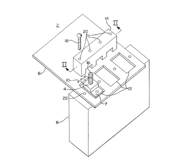
Figure 1 is a perspective view of one embodiment of a semiconductor
device mounted to a heat dissipater according to the present invention;
Figure 2 is a sectional view of the mounting system for a semiconductor
device of the present invention taken along line II-II;
Figure 3 is a sectional view of an alternate embodiment of the present
invention showing a flat load spring;
Figure 4 is a sectional view of an alternate embodiment of the present
invention showing a retaining block having end clips which engage the heat
sink;
and
Figure 5 is a graph showing the relationship between clamping load and
thermal impedance.
Description of the Preferred Embodiment
Now referring to Figure 1, a semiconductor device mounting system 2 is
shown where a semiconductor device 4 which produces high temperatures when
in operation is mounted within a board opening 12 formed in a printed circuit
board
6 where the heat transmitting surface 7 of the semiconductor device is in
direct
contact with a thin thermally conductive mounting pad (not shown) which acts
as an
electrical insulator which contacts and conducts heat to a heat dissipater
such as
a heat sink 8 which is commonly made out of a high thermal conductivity
material
such as aluminum and acts to dissipate excess heat into the surrounding air or
into
a cooling fluid. The thermally conductive electrical insulator (thermal pad)
is
commonly a thin sheet of silicone filled with a heat conducting material such
as
-4b- 2 0 9 7 0 9 7
aluminum oxide.
Three semiconductor devices 4 are shown in Figure 1, although any
number of devices can be mounted sequentially in a similar manner using the
method of the present invention.
The semiconductor device 4 commonly has a plurality of electrical
connection leads 10 which are electrically and mechanically attached to the
printed
circuit board 6 by soldering to connection pads. The connection pads
209709?
-5-
are then electrically connected to the devices (not shown) located on the
printed circuit board 6.
The circuit board openings 12 are formed so as to allow the
semiconductor device 4 to pass therethrough and come in contact with the
heat sink 8 via the thermal pad. A retaining block 14 is used to retain and
locate a load spring 16 such that the load spring 16 is compressed when the
retaining block is bolted to the heat sink 8 by engaging a plurality of
threaded
holes in the heat sink 8. The holding bolts 18 pass through a corresponding
number of mounting bolt holes 20 in the retaining block 14 extending
therethrough and engaging and threading into the heat sink 8. The circuit
board 6 is clamped and held between the retaining block 14 and the heat sink
8.
The load springs 16 which are shown as coil springs, but can be
any type of spring, are compressed when the retaining block 14 is attached
using the holding bolts 18 or any other type of fastener and introduces a load
against each respective semiconductor device 4 which is forced against the
heat sink 8 thereby permitting maximum heat transfer through the heat
transmitting surface 7 through the thermally conductive electrical insulator
and
into the heat sink 8. Other types of springs could be used such as a
flat~metal
spring. Any load generating means to introduce a clamping force to produce
a high contact pressure between the semiconductor device heat transmitting
surface 7 and the heat sink 8 can be used.
Figure 2 is a sectional view of the retaining block 14 taken along
line II-II shown in Figure 1. Figure 2 shows a plurality of load springs 16
where
spring pockets 24 are formed into the retaining block 14 allowing the load
springs 16 to be located therein. Also shown is the mounting bolt holes 20
which allow the mounting bolts 18 to pass through and then through the board
mounting holes 22 and then thread into tapped holes in the heat sink 8.
The heat sink 8 can be a variety of geometries and can consist
of fins which extend from the area where the printed circuit board is mounted.
The heat sink 8 can also be cooled with the introduction of a forced flow
liquid,
such as water, which is well known in the art.
._ 209'~09~
-s-
The retaining block 14 can be made of a material such as a plastic
which is easily molded and/or machined to include the spring pockets 24 and
the mounting bolt holes 20. In the aftemative, a metal material could be used
for increased strength and some additional heat transfer. The load springs 16
are made of a spring steel and are selected to provide the desired clamping
load of the semiconductor device 4 to the heat sink 8 via the thermal pad by
selecting the length and diameter of the spring coils depending on the
specific
geometry of the semiconductor device 4, the depth of the spring pockets 24
relative to the surface of the circuit board 6 and the overall diameter of the
load
spring 16.
Using the mounting methods disclosed in the present invention)
high clamping loads can be attained to force the semiconductor device 4
against the heat sink 8 via the thermal pad for improved thermal transfer and
improved cooling. The semiconductor device 4 to be cooled is commonly a
commercially available surface mount device such as a field effect transistor.
Figure 3 discloses an alternate embodiment of the present
invention where the coil spring used for the load spring 16 has been replaced
with a flat spring 26 which is bent into a U-shape where, upon installation of
the
retaining block 14', the flat spring 26 is compressed against the
semiconductor
device 4 thereby providing a force on the semiconductor device 4 clamping it
against the heat sink 8 via the thermal pad which acts as a heat dissipator.
The
retaining block 14' has been altered to include an extended section 27 that
retains the flat spring 26 in the proper position over the semiconductor
device
4. The retaining block 14' is secured in position and compressed using a
plurality of mounting bolts 18 threaded into the heat sink 8.
Figure 4 shows an alternate embodiment of the retaining block
14" where the retaining block 14 or 14' is modified at each end to include end
clips 28a and 28b which engage a flange portion 30 on the heat sink 8 thereby
compressing load springs 16 in a fashion similar to that shown in Figure 1.
This alternate embodiment allows for manufacture with an ease of assembly not
allowed when a plurality of holding bolts 18 are threaded into the heat sink
8.
Again, similar to Figures 1 and 2 the printed circuit board 6 has
209709'
-7-
a board opening 12 for each semiconductor device 4 formed so that the
semiconductor device 4 passes through the circuit board 6 and comes in direct
contact with the clamping load and through the thermally conductive electrical
insulator (thermal pad) fo the heat sink 8 with the circuit board 6 positioned
between the retaining block 14 and the heat sink 8.
Figure 5 is a graphical representation of the relationship between
the clamping force and the thermal impedance of the interface between the
heat transmitting surface 7 of the semiconductor device 4 and the heat sink 8
through the thermal pad. The desired clamping force of approximately 25
pounds-force (Ibsf)) shown as point 32, can be produced using the techniques
of the present invention by selecting the proper spring rate and overall
spring
height. As shown in Figure 5, the thermal impedance (degrees centigrade per
watt) decreases rapidly, allowing for improved heat transfer between the
semiconductor device 4 and the heat sink 8 as the clamping force is increased
from zero to 10 Ibsf. A force exceeding 30 Ibsf does not greatly decrease the
thermal impedance.
Using the present invention, a multiplicity of semiconductor
devices 4 passing through a like number of open sections in a circuit board
can
be attached and mounted with an ideal level of clamping force to a heat sink
8 with minimal components and relaxed geometric tolerances.
It will be appreciated by those of ordinary skill in the art that many
variations in the foregoing preferred embodiments are possible while remaining
within the scope of the present invention. The present invention should thus
not be considered limited in the preferred embodiments or the specfic choices
of materials, configurations, dimensions, applications or ranges of parameters
employed therein.