Note: Descriptions are shown in the official language in which they were submitted.
2097179
WO 92/10059PCr/US9l/08649
, I_
ELECTRO-OPIICAL IMAGING ARR~Y WITH
MOTION COMPENSATION
BACKGROUND OF THE INVENTION
A. Field of the Invention
5This invention relates generally to motion compensation in im~ging
systems. More particularly, it relates to improved techniques which
electronically compensate for the relative motion of an image of a scene
with respect to an electro-optical im~ging array suitable for carriage by a
reconn~ics~nce vehicle.
B. Back~round Art
Most people who have attempted to photograph a rapidly moving
object at close range with a simple box camera have found that the film
image of the object is blurred or smeared due to the relative motion of the
image over the film. The same effect is observed if the camera is moved
15 during exposure of a stationary scene. If light conditions permit very short
exposure times, the image essentially can be "stopped" by increasing shutter
speed, and the smearing can be minimi7ed.
Reconn~ics~nce cameras frequently are required to record images in
light conditions that prevent sufficiently short exposure times to elimin~te
20 image smearing by increases in shutter speed alone. Typically, such
cameras are carried by aircraft for recording terrain scenes. ~m~ging
systems used in such cameras comprise not only film, but also electro-
optical devices, including charge-coupled devices. In any such camera in
which relative motion exists between a scene to be imaged and the im~ging
25 system, the recorded image of the scene will be smeared unless some
technique is used to compensate for the relative motion. Such techniques
commonly are known as "forward motion compensation" or "image motion
compensation." Left uncompensated, the smearing and image degradation
209717~
Wo 92/10059 PCr/US91/08649
-2-
reslllting from the relative motion reduces the information content of the
recorded image.
When a scene of interest is directly below an aircraft, the rates of
motion of all points of the scene image in the field of view are nearly the
same, and the motion can be compensated to avoid smear relatively easily.
For example, if the im~ging system is film, smear is avoided by moving the
film emulsion at the same rate and in the same direction as the motion of
the scene image in the focal plane of the camera.
When the scene of interest is not directly below the aircraft, but is
perpendicular to the direction of flight and at an oblique angle, the solution
to the problem of image motion compensation becomes difficult, principally
because objects at a closer distance to the aircraft appear to be moving
faster relative to the aircraft than objects farther away. Similarly, when the
scene of interest is forward of the aircraft, the solution to the problem of
image motion compensation becomes more difficult because terrain farther
ahead appears to be moving slower than terrain closer to the aircraft.
The specifics of the problem are modified when changes in the
aircraft velocity, height above ground, or camera depression angle occur.
These changes affect the rate of image motion in the focal plane of the
camera, and they must be taken into account by a forward motion
compensation system. The extent of image smear is most directly a
function of the aircraft velocity relative to the ground (V), the height above
ground (H), and the time period of exposure. The extent of the image
smear is also a function of the m~gnit~lde of the field of view and the
angle of depression below the horizontal where the field of view is located.
Mechanically-based forward motion compensation schemes have been
devised and implemented in an attempt to elimin~te image smear due to
forward motion, or to reduce such smear to acceptable levels. Such
schemes have been implemented by use of a tr~n~l~ting film, a tr~n~l~ting
lens, or a rotating mirror.
2097179
WO 92/lO059 PCr/US91/08649
-3-
In the tr~ncl~ting film technique, the film is moved in the same
direction and velocity as a portion of an image. The image motion velocity
(Vj) and the film velocity (Vf) are made essentially synchronous and
relative motion between them during the exposure time period essentially
is elimin~te~l The net result is that the image portion is essentially
stationary with respect to the film during the exposure time period. The
tr~n~l~tin~ film technique is frequently used on short and medium focal
length framing type cameras.
In the translating lens technique1 if a lens is tr~n~l~ted in space, the
image of distant objects vill translate with the lens in a one-to-one
relationship in the same direction. Therefore, if the lens in an aerial
camera is translated at the proper velocity opposite to the direction of
flight, the image velocity caused by the aircraft forward motion is cancelled
by the image velocity due to the moving lens. The net result is that the
image is essentially stationary relative to the film, and therefore no
essential motion smearing is occurring during the exposure. This type of
forward motion compensation is frequently used on short and medium focal
length panoramic type sc~nning cameras. See, e.g., Ruck, Design Versatility
of the Prism Panoramic Camera: The KS-116 and KA-95 Cameras, SPIE
Proceedings, Vol. 309, paper 309-10, (Aug. 27-28, 1981).
In the rotating mirror technique, as the aircraft is flying in a given
flight path, the objects in the scene have an apparent ~nF~ r velocity
relative to the camera. The apparent ~n~ r velocity is related to the
airaaft velocity and the range to the target. If a camera is looking into
a mirror at a nominal angle of 45, the camera line of sight is deviated by
a nominal 90 angle. If the mirror is rotated in the proper direction and
at the proper rate during the exposure, the scene appears to have no
motion relative to the camera. Therefore, at the film plane, the image is
essentially stationary and forward motion image smear is substantially
2097179
WO 92/10059 ~ PCr/US91/08649
-4-
negated. The rotating mirror forward motion compensation concept is
often used on long focal length frame and line sc~nning type cameras.
All three of the foregoing mechanical forward motion compensation
srhem-os are employed in various aerial reconn~iccance cameras, inclll~ing
S film cameras and electro-optical line sc~nning cameras. A principal
disadvantage of these forward motion compensation schemes is that they
all involve mechanical devices and consequently add complexity, weight, and
expense to the im~ging system.
Other methods and techniques of forward motion compensation also
have been developed. In the Prinz patent, U.S. Patent No. 4,505,559, a
mechanical image motion compensation technique is disclosed wherein a
slot on a focal plane shutter moves in a direction transverse to the
direction of film transport, while the direction of film transport is made
parallel to the direction of flight. In order to compensate for a component
of image motion, the slotted shutter is coupled to an encoder which, in the
course of m~king an exposure, reports to a computer for instantaneous field
position of the shutter slot. The computer determines the speed profile in
the interval between successi~e exposures and issues a control signal to
regulate the film drive.
The Gordon et al. patent, U.S. Patent No. 4,157,21~, discloses a wide
angle sc~nning reconn~ics~nce camera which uses a wide angle lens and a
curved exposure slit disposed adjacent an image receiving surface, typically
film. The exposure slit is crescent shaped to correspond to equal points of
equal range so that there is negligible differential image motion within the
slit, and the slit is of constant width in the direction of vehicle motion.
The image receiving surface (e.g., film) is driven in the direction of vehicle
movement at a speed corresponding to the altitude-velocity ratio of the
vehicle with respect to the object field.
The Wight patent, U.S. Patent No. 4,908,705, discloses an electro-
optical aerial reconn~i~s~nce system wherein a linear charge-coupled device
2~97~79
WO 92/10059 PCr/US9l/0~649
-5 -
imager is movably positioned in the focal plane of a fixedly mounted wide
angle lens system. The linear imager is moved in the fore and aft
direction in the same direction as the apparent motion of the image to
reduce the apparent image motion and consequent smear. This system,
however, only is ~esi~ned for im~ing terrain at nadir, aft of nadir or ahead
of nadir, and does not provide forward motion compensation in a side-
oblique reconn~i~s~nce application.
For aerial reconn~ic~nce, electro-optical cameras, particularly those
of the charge-coupled device variety, are perceived as superior to film
cameras to an increasing extent. In an electro-optical camera, radiation
from an image of interest impinges on a solid state device typically having
several thousand (at least) picture elements or pixels. The incident
radiation is converted into charge packets (pixel information) at the
photosites (pixels) and is collected in potential wells. The charge packets
contain scene information, and upon being transferred out of the device,
are converted into electrical si~n~ls The primary advantage of an electro-
optical im~gin~ camera is that the scene information can be almost
instantaneously "downloaded" &om a reconn~iss~nce aircraft to an earth-
based station, or can be converted to a video image. Since charge-coupled
device im~in~ cameras have very small pixels closely spaced together, the
resolution of a resulting image tends to be very high. Electro-optical
im~ing cameras can be made sensitive to particular frequencies of incident
radiation. Background information on charge-coupled devices can be found
in standard texts such as D. Schroder, Modular Series On Solid State
Devices, Ch. 3, 4, Addison-Wesley (1987), and in C. Sequin and M.
Tompsett, Char~e Transfer Devices, Bell Telephone Laboratories, Academic
Press (1975), and in S. M. Sze, P~lysics of Semiconductor Devices, Ch. 7,
John Wiley & Sons, Inc. (1981).
In a linear electro-optical focal plane reconn~i~s~nce detector, such
as the linear-detector of the Wight patent, a scene of interest is scanned
209717~
WO 92/lO059 PCr/US91/08649
~ ~ -6-
a line at a time across an array in a direction perpendicular to the array
length. Rec~se the means of sc~nning is provided by the aircraft forward
motion, the aircraft must m~int~in a steady, well defined flight path while
the scene is being recorded. Depending on the size of the scene, the
recording time for any one target may range between 10 and 20 seconds,
or even longer. In a military situation in which the reconn~ics~nce aircraft
may be subject to enemy threats, the vulnerability during the recording time
may be excessive.
To reduce the time needed to image a scene of interest and thus
reduce the time of exposure to hostile threats, a preferred mode of the
present invention uses a two-dimensional electro-optical im~ging area array,
rather than a linear (one-dimensional) array. An area array can image an
entire scene inct~nt~neously, rather than a line at a time. Until recently,
only relatively small electro-optical im~ging arrays have been commercially
available, and are typically used in television cameras. But large, high pixel
count area arrays suitable for aerial reconn~ics~nce sensors are now
entering the realm of feasibility. Two scientific images used in
astronomical applications, the Tektronix TK 1024 CCD and the Ford
Aerospace 4,096 x 4,096 pixel element array, can be adapted to the present
invention by subdividing the arrays in column groups and providing the
circuitry for faster frame rates. Information useful for designing high pixel
count area arrays also is found in J. Janesick, Multi-Pinned-Phase Charge-
Coupled Device, NASA Tech. Brief Vol. 14, No. 8, Item No. 115, p. 22, Jet
Propulsion Laboratory, August, 1990.
An area t,vpe detector array can convert an entire image of a scene
into a complete frame of pixel information during a short exposure period,
typically on the order of a hundredth of a second. After the exposure
period, a shutter can be used to prevent continued exposure while the pixel
information in the array is read-out to a signal processing unit. After the
read-out is completed, the array is ready for the next frame exposure. If
2097179
WO 92/lO059 PCr/US9l/08649
-7-
the frame read-out time is short (much less than a second), then
consecutive frames can be taken in sub-second intervals in order to obtain
large scene coverage in short periods of time. By providing motion
compensation in an area detector having exposure time controlled by a
shutter, the present invention substantially reduces exposure of an aircraft,
a pilot and a detector array to enemy counterme~cllres.
The motion compensation techniques of the present invention also
enable effective use of a detector array having a large number of photosites
or pixels (e.g., four to six thousand or more in both the columns and rows
of the array) that will image a large area of terrain in every frame. The
present invention makes such arrays practical by preserving image resolution
(ie., scene detail information) in every frame of imagery. The present
invention also enables high array exposure sensitivity. That is, motion
compensation is accomplished in a way that promotes long exposure time
without blurring the image. In a pushbroom system, exposure time is
limited by the line rate which is dictated by the aircraft velocity to height
ratio (V/H). For the present invention the exposure time is not limited by
the aircraft V/H. This permits operation at lower scene illllmin~tion levels
and extends the available time of day for light-sensitive sensor operation.
Additionally, the present invention provides for rapid read-out of
collected scene information. A rapid read-out of the electrical signals of
an array is necessary in order to achieve high frame rates. High frame
rates are desirable to allow multiple images to be recorded in a short time
such as required for stereo imagery.
The present invention offers additional advantages over linear
electro-optical sensors. For example, motion compensation is provided
irrespective of whether an electro-optical im~ging array is deployed in a
side oblique, forward oblique, or down-looking application. The present
invention also provides lower scene distortion and true stereo imagery
30 capability. By using the present invention to replace a film camera
2097179
Wo 92/10059 PCr/US91/08649
-8-
mounted in an aircraft, motion compensation can be accomplished while
retaining similar exposure times and aircraft maneuverability characteristics.
The present invention is reliable and robust because it requires no
mechanical sc~nning mech~nicm, no rotating mirrors and no tr~ncl~ting
lenses in order to achieve forward motion compensation.
Another feature of the invention is that it is suitable for use in a
wide variety of applications, such as tactical reconn~ics~nce, drug
interdiction, low intensity conflict, low and medium altitude missions, and
reconn~ics~nce at low light levels.
2097179
WO 92/10059 PCI/US91/08649
g
SUlVlMARY OF THE INVENTION
These and other objects, advantages, and features of the invention
can be achieved by providing techniques for processing pixel information
representing an image of a scene which compensate for image motion in
5 a predetermined direction. An array of cells is used to store pixel
information representing the image. The cells (photosites or pixels) are
arranged in rows and columns and are suitable for carriage by a vehicle
capable of motion in the predetermined direction. The columns are
organized into one or more columns groups, and pixel information (charge
10 packets) located in the one or more groups is transferred at one or more
predetermined transfer rates depending on the rate of motion of portions
of the image relative to the array. The transfer rates preferably
correspond to the rate of image motion in the focal plane of the array.
One or more predetermined transfer rates can be adjusted depending on
changes in the rate of motion of the vehicle and other parameters. In
operation, the predetermined transfer rates for the pixel information in the
column groups are adjusted to be as close as possible to the rates of image
motion in the column groups. By using the foregoing techniques, resolution
of the image created from the pixels is preserved, and image smear from
20 the forward motion of the vehicle is substantially reduced.
One embodiment of the invention uses a shutter and lens system.
The shutter opens during the time for exposure of the array, and the lens
focuses the image of the scene onto the array. Pixel information is
transferred by means of a master clock which issues signals at a master
25 clock frequency, and by means of a plurality of drive and control circuits
responsive to the signals from the master clock. Each of the drive and
control circuits transfers pixel information in one of the column groups.
The drive and control circuits include a counter and a clock driver.
The clock driver transfers pixel information in all the columns in a column
30 group when the counter counts a predetermined number of counts. The
2097179
WO 92/10059 PCr/US91/08649
-10-
number of counts for each column group is related to the predetermined
transfer rate for each column group, which in turn is a function of various
parameters that can include the velocity to height ratio and the focal length
of the lens, as well as the distance from the array to the points of the
5 scene to be imaged, and other factors to be discussed below.
According to one embodiment of the present invention, charge
transfer from pixel to adjacent pixel occurs in the direction of image
motion during the time of scene exposure. The rate of charge transfer in
the column groups across the array varies from group to group so that
charge transfer rate and the image motion velocity can be synchronized (in
discrete steps) across the entire array when the array is deployed in a side
oblique orientation. As a result, "graded" forward motion compensation can
be embodied in an advanced electro-optical sensor with no moving parts.
In a forward oblique mode of operation, image motion in the focal
15 plane of the array does not vary across the columns of the array.
Nonetheless, image motion compensation in the forward oblique mode is
similar to that of the side oblique mode. However, instead of varying the
transfer rate of pixel information across the array from one column group
to another, the transfer rates are the same across the columns of the array.
WO Y2/1~U59 2 0 9 7 1 7 9 PCr/US9~/û8649
BRIEF DESCRIPTION OF THE DR~WINGS
The preferred embodiment of the present invention will be described
in conjunction with the accompanying drawings, in which:
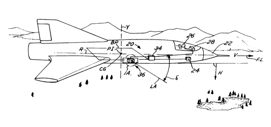
FIG. lA is a simplified schematic drawing of an airborne
reconn~iss~nce system utilizing an electro-optical camera assembly made
according to a preferred form of the present invention and showing the
interrelationship between the system components;
FIG. lB is an enlarged, fragmentary perspective drawing of the
camera assembly of FIG. lA showing the relationship between various
components, including an electro-optical im~ging array;
FIG. 2 is a schematic drawing of a reconn~iss~nce aircraft operating
in a side oblique mode and illustrating the focal plane of the camera
assembly of FIG. lB greatly enlarged and displaced in order to clearly
show the relationship between the focal plane and a scene of interest;
FIG. 3 is a schematic drawing of the im~ging array of FIG. lB
showing the arrangement of the array in rows and columns, the
org~ni7~tion of the columns into a plurality of column groups and the
transfer of pixel information in each group at different predetermined
transfer rates;
FIG. 4 is a block diagram of a preferred form of electronics and
control circuitry that operates the electro-optical im~ging array of FIG. lB
according to the te~c~lings of the present invention;
FIG. 5 is a block diagram of the drive and control circuitry shown
in FIG. 4, illustrating the counter and clock drivers which transfer pixel
information in each of the column groups of the imaging array shown in
FIG. 3;
FIG. 6 is a schematic, block diagram of a counter and clock driver
for an arbitrary column group of the im~ging array of FIG. 3;
FIG. 7 is a schematic drawing of one section of an arbitrary column
group showing the metalization on top of the channel stop region between
2097179
WO 92/10059 PCr/US91/08649
-12-
photosites of the array to provide the three-phase drive clocking to the
column group;
FIG. 8 is a cross-sectional view of one section of the column group
of FIG. 7;
FIG. 9 is a schematic drawing of a reconn~ic~nce aircraft operating
in a forward oblique mode and illustrating the focal plane of the camera
assembly of FIG. lB greatly enlarged and displaced in order to clearly
show the relationship between the focal plane and a scene of interest;
FIG. 10 is a schematic diagram of a side oblique reconn~icc~nce
application of the present invention, showing the time advantage of the
electro-optical camera assembly of FIG. lB as compared to a prior art
linear assembly; and
FIG. 11 is a schematic diagram of a side oblique reconn~ics~nce
application of the present invention illustrating how stereo scene coverage
can be obtained using the electro-optical camera assembly of FIG. lB.
2~97179
WO 92/tOOSg PCI-/US91/08649
-13-
DESCRIPIION OF THE PREFERRED
EMBODIMENT OF THE INVENTION
Referring to FIG. 1, a preferred form of electro-optical system
according to the present invention comprises part of a reconn~ic~nce
5 system 20 installed in an aircraft 22 that defines orthogonal roll, pitch and
yaw axes R, PI and Y, respectively, each passing through a center of gravity
CG. The roll and pitch axes define a bilateral plane BP that is horizontal
during level flight. System 20 includes a camera assembly 36 defining a
lens axis LA that can be directed toward a scene of interest.
Aircraft 22 has an avionics system 24 which provides to system 20
input signals indicating aircraft ground velocity (V), aircraft height above
ground (H), and aircraft roll, pitch and yaw angular position data. From
console 28, an operator 26 provides additional inputs into system 20, such
as the depression angle ~ between axis LA and plane BP. The inputs from
the avionics system 24 and console 28 are fed to a camera control
computer 34 which processes the inputs, together with pre-flight
programmed information, and generates control signals for camera assembly
36.
Referring to FIG. lB, camera assembly 36 includes an im~gin~ array
32 tlefining a focal plane FP having a center point CE. Camera assembly
36 also includes a housing 38 and a lens 40 having a focal length F (not
shown in FIG. lB) and defining axis LA that passes through point CE. A
shutter 41 is provided to selectively expose array 32 to radiation from the
scene. Typically, housing 38 iS isolated from the aircraft 22 in order to
reduce vibration or other high frequency, low-amplitude motions. Printed
circuit cards 39 incorporate the electronics that support operation of array
32.
FIGs. 2 and 3 illustrate a preferred technique of "graded" forward
motion compensation that is a principal feature of the present invention.
Fig. 2 shows aircraft 22 carrying the camera assembly 36 operating in a
2097179
WO 92~10059 PCr/US91/08649
-14-
side oblique mode, m~which-focal plane FP of im~ging array 32 is oriented
parallel to a line of flight vector FL coincident with roll axis R that defines
the direction of motion of aircraft 22 and array 32. Referring to FIGS. lB
and 2, focal plane FP defines a plane PFL that is collinear with axis LA,
passes through center point CE and is perpendicular to plane FP and
vector FL. Focal plane FP also defines another plane PS that is collinear
with axis LA, passes through center point CE and is perpendicular to
planes FP and PFL and parallel to vector FL. Aircraft 22 flies over the
terrain at velocity V and at height H. In order to image a scene 42, lens
axis LA and plane PS of array 32 (FIG. lB) are oriented at depression
angle ~ with respect to plane BP (FIG. 2).
Lens 40 focuses scene 42 onto im~ging array 32, which is placed at
the focal plane FP of the lens. The boundary of the scene is defined by
points A-D, and the corresponding points .n plane FP are shown with like
letters. The rate of image motion is not constant throughout the array, but
rather is dependent upon the range or distance R between lens 40 and the
points of the scene lying in plane PFL. The greater the range, the slower
the rate of image motion in focal plane FP of the lens. More specifically,
the rate of image motion in the array at an arbitrary point, Vi, is equal to
(F/cos e)(V/Rj), where e is the field of view half angle, and Rj is the
range between the lens and the terrain point corresponding to the point Vj.
Since focal length F normally is very small compared to range Rj, Rj can
be ap~ro~i..,~ted by using the distance between the terrain point and the
array or aircraft. As shown in FIG. 2, if point 44 on the terrain farthest
25 from aircraft 22 is chosen (ie., the midpoint of line segment CD), the
image velocity v1 is equal to (F/cos e)(V/R,).
It can be shown that Rj = H/sin (~ + e), so
V; = F (~) sin (~ + e)
(H) cos e
WO 92/10059 2 ~ 9 71 7 9 PCr/US91/08649
Similarly, it follows that the image velocity in the array for point V,
(col,esponding to terrain point 46) is F(V/H)(sin ~) and for point V3
(corresponding to terrain point 48) is
F (V/H) (sin ~ + e).
S cOs e
To compensate for the fact that the image motion varies across the
array, the preferred form of the present invention implements a "graded"
forward motion compensation technique whereby array 32 is organized into
a plurality of column groups, and charge is transferred from pixel to
adjacent pixel in the direction of image motion during the time period of
scene exposure. The rate of charge transfer is made variable in the
direction transverse to the image motion, ie., across the column groups of
array 32. Thus, by synchronizing the charge transfer velocity and the image
motion velocity in discrete steps across the array, graded forward motion
compensation is achieved electronically with no moving parts. Ideally, each
column of pixels would have its own column transfer rate. However, for
many applications, it is sufficient to organize the array into a discrete
number of column groups and to transfer charge at a uniform rate in all
the columns of an individual column group.
Referring to FIG. 3, the boundary of the image of scene 42 on array
32 is indicated by points A-D which correspond to the like lettered points
of scene 42 (FIG. 2). Width W of array 32 preferably is 48 to 60 mm and
represents 4000 to 6000 pixels. Length L of array 32 preferably is 48 to
60 mm and represents 4000 to 6000 pixels. Only a few of the pixels 51 are
shown schematically in FIG. 3. The pixels of array 32 are divided into
rows and columns, and the columns, in turn, are organized into a plurality
of column groups 50. The number of column groups selected may vary
depending on the operational parameters of the system, the degree of
resolution required, and the desired cost to performance ratio. It has been
found that 16 column groups provide a very high level of forward motion
WO 92/10059 2 ~) 9 7 1 7 9 PCI/US91/08649
-16-
compensation for array 32 and are an acceptable number of groups in an
array having appro~rim~tely 5,000 individual columns. Still referring
to FIG. 3, each column group 50 has its own separate variable charge
transfer rate (generally measured in pixels/second) depending on the image
motion rate at the center of the column group. The variable charge
transfer rates are represented as arrows, and the longer arrows represent
faster rates. Referring to FIG. 3, and the example in FIG. 2, column C16,
which images the terrain closest to line AB (FIG. 2), has the fastest charge
transfer rate, since line AB is closest to aircraft 22, and the image motion
appears fastest in that portion of scene 42. The charge transfer rates varv
monotonically across the array. Column C1 which images terrain adjacent
line CD (FIG. 2) has the slowest charge transfer rate.
During the exposure time period when shutter 41 is open, charge
representing scene information is collected in pixels in array 32 and is
transferred from one adjacent pixel to another according to the transfer
rates in the column groups. When the exposure time period ends (ie.,
when shutter 41 is closed), the accl-m~ ted charge representing the scene
is sequentially read out of array 32 one row at a time into readout registers
S2A-52D. From readout registers 52A-52D, the information is fed to signal
processing equipment for evaluation by a user. When the readout is
complete, array 32 is ready for the next scene exposure.
Referring to FIG. 4, camera assembly 36 and its associated control
circuitry are illustrated in block diagram form. Avionics system 24 provides
velocity and height information over a bus 25 as inputs to camera control
computer 34. From console 28, the operator inputs into computer 34 over
a bus 29 the depression angle ~ in degrees (FIG. 2). Stored in computer
34 are mission parameters that are previously determined, e.g., focal length
F of lens 40, the mode of operation (side oblique or forward oblique), the
size of array 32, number of column groups, pixel size, and a control circuit
master clock frequency (discussed below).
WO 92/10059 2 0 9 7 l 7 9 PCI/US9l/08649
After procescing the data inputs, computer 34 transmits signals over
a bus 35 that enable lens axis LA of camera 36 to be directed to the
desired orientation, transmits signals over a bus 37 that controls the frame
exposure time period by enabling opening and closing of shutter 41, and
transmits comm~nd signals over a bus 64 to drive and control electronics
54. Drive and control electronics 54 transrnits over a bus 68 signals that
organize the columns of array 32 into one or more groups and that transfer
pixel information located in the one or more groups at one or more
predetermined transfer rates. Computer 34 functions as a means for
adjusting the one or more predetermined transfer rates depending on the
velocity of the aircraft, the height above the terrain, the depression angle
and possibly other parameters. A master clock 58 issues pulses over a
conductor 59 at a predetermined master clock frequency to drive and
control electronics 54. Alternatively, the master clock pulses may be
supplied by coll,~uter 34.
Scene information in im~ging array 32 is fed over a bus 53 to a
signal proces~ing unit 56 which, in turn, sends the information over a bus
55 to a recording or viewing device 57, or to a data link for tr~n~mi~sion
to a remote location. Signal processing unit 56 also provides exposure
control feedback to computer 34 over a bus 61 so that the frame exposure
time may be adjusted to optimize signal collection.
Referring to FIG. 5, drive and control electronics 54 is shown in
greater detail and illustrates the alternative embodiment in which master
clock pulses are provided by computer 34. For column groups C1-C16 of
array 32, counters CN1-CN16 and corresponding clock drivers CD1-CD16
are provided. The outputs of counters CN1-CN16 are connected to the
inputs of clock drivers CD1-CD16 by conductors CO1-CO16, respectively.
Representative counter CN1 for column group C1 receives inputs over
colllputer data bus 64, including pulses from a master clock located inside
computer 34, a frame start/stop signal, and a pre-load signal representing
WO 92/loosg 2 ~ 9 7 17 9 PCI/US91/08649
-18-
a counter value which is related to the charge transfer rate for column
group C1. When counter CN1 counts to the counter value, a trigger signal
is sent by the counter to clock driver CD1 over conductor C01. Clock
driver CD1, in response to the trigger signal, transfers pixel information in
5 all the columns in column group C1 by one row in array 32 by issuing
voltage pulses over 3-phase output bus 68. This process of counting to a
counter value and triggering a clock driver may repeat any number of times
during the scene exposure depending on the rate of image motion in plane
FP of array 32 (FIG. lB). The faster the rate of image motion in the
plane of the array, the more times the counting and triggering cycle must
be repeated in order to synchronize the image motion with the array charge
motion.
Still referring to FIG. 5, signals from camera control computer 34
travel via data bus 64 to each of the counters CN1-CN16 for each of
lS column groups C1-C16. Each of clock drivers CD1-CD16 provides one set
of 3-phase clocking output lines 0~, 02 and 03 per column group. In FIG.
5, the subscript of a clocking output line identifies the corresponding
column group within column groups C1-C16.
FIG. 6 shows isolated an arbitrary column group Ci (50) and its
20 associated counter CNi and clock driver CDi. For purposes of illustration,
column group Ci is composed of 384 individual columns. In order to
ensure that all array rows in a column group are transferred simultaneously
when a related counter triggers a corresponding clock driver, the 3-phase
clocking must be provided to all rows of the column group. This is shown
25 symbolically by the 3-phase output lines 68 of clock driver CNi extending
the length of column group Ci so that each row of column group Ci
receives the 3-phase clocking pulses.
Assuming the clock drive circuits are not fabricated on the im~,ging
array, 3-phase output bus lines 68 must be bonded to separate package pins
WO 92~10059 2 0 9 717 9 PCI/US91/08649
-19-
for external drive control. Thus, the number of vertical clock drive pins for
array 32 is three times the number of column groups.
FIG. 7 shows in enlarged detail one portion of an arbitrary column
group Ci of im~ging array 32. In particular, part of column group Ci is
S shown adjacent part of a neighboring column group Ci-1. Column group
Ci is composed of S,000 rows of photosites 85 and 384 columns design~ted
CL1-CL384. Each photosite (shaded region) is bounded by a p+ channel
stop 70, which separates each column from the next. Polysilicon horizontal
lines 72 subdivide the photosite and bus the 3-phase clocking signals across
the column group. The vertical clock drive pins 74, 76 and 78 are
connected to metallization lines 80, 82 and 84, which run the entire length
of the column group.
Metal to polysilicon contacts 86 on top of the channel stop regions
70 are provided periodically every third holi;contal line throughout the
length of the column group for each metalli7~tion line to provide the
voltage pulses for each row of the array. The 3-phase clocking signals
(voltage pulses) may confine individual photosite charge vertically or may
provide for the vertical transfer of these charge packets. Column groups
Ci and Ci-1 are separated from each other by providing a break 88 in the
polysilicon horizontal lines 72.
FIG. 8 is a simplified cross-sectional view of the array of FIG. 7
along the line AA'. The polysilicon horizontal lines 72 are pulsed by the
3-phase clocks 01~ 0,. 03, c~llsing charge packets collected in potential
wells 75 in a p-type silicon substrate 71 to be shifted down the array. In
FIG. 8, the polysilicon horizontal lines 72 are isolated from each other by
a SiO, layer 73. Another SiO, layer 77 also separates the polysilicon
horizontal lines 72 from substrate 71.
The charge-coupled device architecture shown in FIG. 7 is essentially
a full frame imager configuration. The full frame configuration provides
a large area array which provides a high percentage of silicon wafer area
WO 92/10059 2 0 9 7 1 7 9 PCI/US91/08649
-20-
available for light collection. By contrast, a frame transfer architecture
requires a frame storage région which occupies applo~nlately the same
amount of silicon wafer area as the im~ging area. The interline transfer
architecture is not as desirable since it does not provide the image
resolution and small pixel pitch of the full frame design. The interline
transfer architectnre also requires a vertical transport register which adds
non-sensitive spacing between adjacent pixels, reducing fill-factor and
resolution. An X-Y addressable charge injection device is another possible
architecture for the present invention, but it, too, is considered not as
desirable. A discrete array of diode detector elements is also a possible
architecture for the invention. Such an array or the above-mentioned
architectures could operate in the ultraviolet, visible, or infrared spectral
regions. Nevertheless, the te~rhings disclosed herein can be readily adapted
to these architectures should they be preferred for other reasons, and the
lS scope of the present invention is intended to cover these alternative
architectures.
System Operation
Referring to FIGS. lA - 5, the operation of the im~ging array in a
side oblique mode to provide graded forward motion compensation will be
first ~ lc~ed. Pre-mission programmed information is supplied to camera
control computer 34, and includes:
F = focal length of lens 40;
m = im~ging array width perpendicular to the charge transfer
direction (ie., width W, FIG. 3);
~ = number of array column groups;
Px = pixel size, in the charge transfer direction (i.e., direction of the
vertical arrows in FIG. 3);
X = master clock frequency;
FOV = field of view = 2 arctan (m/2F)
WO 92/10059 2 0 9 717 9 PCI/US91/08649
e1 = en = (FOV/2) (N-1/N)
When the operator is ready to begin taking pictures, he or she
selects a depression angle ~ (FIG. 2) to image the terrain scene of interest.
At this time, avionics system 24 provides to computer 34 the velocity and
5 height data.
From these parameters, computer 34 calculates the charge transfer
rate for the first column group (f,) and the charge transfer rate for the Nth
column group (fn) according to:
f~ )(V)(sin (~ + eO
(Px )(H) Cos e
(1)
fn = ~)~V)(sin (~ + en)
(Px)(H) Cos e"
The "+" and "-" above will be opposite for f1 and for fn, and the choice of
lS sign depends on the array orientation. The above equations hold for
depression angles from 0 to 180, where 0 to 90 would be arbitrarily
defined as left oblique and 90 to 180 would be right oblique.
To deterrnine the charge transfer rates for the column groups
between 1 and N, a sinusoidal formula
fj = (F)(V)(sin (~ + e))
(Px)(H) Cos e
could be used, with the values of e calcul~ted to the center of each column
group. However, in the preferred embodiment, a linear approximation
formula is used which yields substantially the same results, with an error
25 factor of about 0.01%. This linear apprnxim~tion formula for the charge
transfer rates for the ith column group is:
(2) fi = fl + (i-1) (fn - f~)/(N - 1)-
After calc~ ting the charge transfer rates for each column group,
the computer then calculates the pre-load counter value for each counter
wo 92/10059 2 ~ ~ ~ 17 9 Pcr/us9l/0864g
CN in drive and control electronics 54 (FIG. 5). These counter values CV
for each counter (and for each column group) are:
CVj = X
fj
S where X is the master clock frequency and fj is the charge transfer rate in
the ith column group. The counters are then pre-loaded with the counter
values over bus 64 (FIG. 5).
When the operator triggers a frame to take a picture, the shutter is
simultaneously opened for an exposure time period calculated by computer
34. In this example, the exposure time period is 0.01 second. At the same
time, each counter in drive and control electronics 54 begins counting at
the frequency X to its pre-loaded counter value. The counting may be up
to the counter value or down to 0 from the counter value. When the
counter counts the predetermined number of counts, a trigger signal is sent
15 from the counter to the clock drive CD for that counter, and one cycle of
3-phase clocking as triggered in the corresponding column group. Pixel
information (electric charge packets) cont~ining scene information is thereby
shifted down one row vertically in all the columns in that column group.
After issuing a trigger pulse to the clock driver, the counter then
20 automatically reloads and begins counting to the counter value again.
When the counter value is reached again, the trigger pulse is sent, the
clock driver shifts the pixel information one row vertically in all the
columns in the column group, the counter reloads and the cycle is
performed again. Meanwhile, the cycles are also being performed in the
25 other column groups. Because each column group has a different charge
transfer rate and corresponding counter value in order to match the charge
transfer rate to the image motion rate, a principal object of the invention
(i.e., electronic forward motion compensation without moving parts) is
realized.
WO 92/lO059 2 0 9 7 1 7 3 PCI/US9l/08649
Although in the preferred embodiment the im~ging array is divided
into 16 column groups as a tradeoff between performance and cost, it may
be desirable to use a 32 or higher column group regime. The more
column groups there are, the less error (image smear) there is at the
boundaries between adjacent column groups. However, with 32 column
groups, there must be twice as many counters and clock drivers, as well as
control lines, in the array. With fewer column groups, e.g., 8, the control
circuitry is reduced proportionately, thus lowering cost, but image smear
near the edges of the column groups may be unacceptable. The size of the
array may be another factor when deciding how many column groups to
use.
Referring to FIG. 2, as an example of system operation, let V = 480
knots, H = 3000 ft., F = 76.2 mm, N = 16, ~ = 30 side oblique, and e
= 22 (field of view = 44). The integration time (exposure time period),
which depends on the light level, is chosen to be 0.01 seconds. The pixel
size is 0.01 mm.
First, the computer calculates f, and f,6 according to equations (1).
Then, from equations (2), the linear approxim~tion formula is used to
calculate the charge transfer rates for the rem~ining ~olumn groups. The
charge transfer rates, fj, are in units of pixels/integration time, or, in otherwords, rows of charge transfer per exposure time period. The results can
be tabulated:
Column Group Char~e Transfer Rate
fj
2S C1 3.554 pixels/integration time (rows
per exposure time period)
C2 4.452
C3 5.349
WO 92/10059 2 0 9 7 17 9 PCI/US9l/08649
-24-
C4 ` 6.247
C5 7.145
C6 8.043
C7 8.940
C8 9.838
C9 10.736
C10 11.634
C11 12.531
C12 13.429
C13 14.327
C14 15.225
C15 16.122
C16 17.020
Using column group 9 for illustration, during the exposure time
period, the image moves 10.736 pixels down each of the columns in column
group C9. Therefore, during the exposure time period, the charge packets
in column group C9 representing scene information must be shifted
vertically down the columns of the column group by 10.736 pixels. More
precisely, the charge packets must be moved by one pixel in the vertical
direction every 0.01/10.736 seconds.
To do this, counter CN9 for column group C9 is loaded with its
particular counter value. If the master clock frequency is 10 MHz, or 100
ns/count, then the integration time of 0.01 seconds results in 100,000
master clock counts in the exposure time period. Thus, the counter value
for colurnn group C9 is 100,000/ 10.736, or 9,314. At the moment of
opening the shutter, the counter, having been set to zero, begins to count
WO 92/l00S9 2 0 9 7 ~ 7 9 PCI/US91/08649
at the master clock frequency up to 9,314. At count number 9,314 a match
is obtained, and the clock driver CD9 (FIG. 5) is triggered. The charge
packets in all the columns of column group C9 then are shifted by one row
vertically. Counter CN9 is reset to zero and begins counting up to 9,314
5 again. Ten cycles of counting and triggering are obtained in 93,140 counts,
and during the remainder of the integration time, no more clock cycles are
triggered.
In the present example, note that if the exposure time period is
reduced to 0.005 second, the image motion becomes 10.736/2 or 5.368
10 pixels during the integration time, and the total of master clock counts
during exposure is halved as well to 50,000. However, the counter value
remains the same. Thus, the exposure period is not critical to the
implementation of the invention, and can be varied by the operator without
affecting the forward motion compensation. The counter values CVj can
be calcul~ted in units of clock cycles per line as X/fj where X is in units
of cycles per second and fj is in units of lines per second. The fj are
derived as in equations (1) and (2), as before.
Folward Oblique Operation
The im~ging array of the present invention is suitable for providing
forward motion compensation in a forward oblique framing mode.
Referring to FIG. 9, the terrain of interest 42 is located directly forward
of aircraft 22. The depression angle ~ represents the angle between plane
BP and lens axis LA that intersects the center of the terrain of interest 42.
In the forward oblique mode, the image velocity across array 32 (ie.,
transverse to the direction of flight) is approximately constant for narrow
fields of view. However, the image velocity at the top of the array is
different from that at the bottom of the array. To m~ximi7e image
resolution, the image velocity near the center of the array is chosen, and
the charge transfer rate down the columns of the array is selected to be
WO 92/10059 2 0 9 717 9 PCI/US91/08649
-26-
synchronized at this rate. This provides a selection which is correct at one
point and a "best fit" compromise for other points in the array. Of course,
other points could be chosen and the charge transfer rate selected to be
synchronized at those points. The image velocity (Vj), and thus the charge
transfer rate, is given by:
Vi = F (O sin2 (~ + ej)
(H)
where F is the focal length of lens 40 and (~ + ej) is the forward
depression angle of the point chosen for synchronization for forward motion
correction.
The charge transfer rate in all the column groups is the same in the
forward oblique mode. Thus, array 32 is organized into one column group.
Computer 34 calculates the charge transfer rate, f, which is given by:
f = (O(O sin~ (~ + ej)
Px H
The counter values for all the counters are the same, and are given by
X
where X is the master clock frequency. After the counter values are
loaded into the counters (FIG. 5) and shutter 41 opens, counters CN begin
counting, and clock drivers CD are triggered. When a match is obtained,
the counters reload, and the cycles are repeated as in the side oblique
mode.
In the forward oblique mode, only one counter and one clock driver
are necessary provided that the clock driver triggers all the columns in the
array. A prior art electro-optical area array that does not have the column
groups disclosed in this specification is readily adaptable to the foregoing
forward oblique motion compensation technique.
A practical advantage of the present invention can be seen in the
illustration of FIG. 10 which represents a hypothetical reconn~icc~nce
scenario in which aircraft 22 is assigned to record the image of an airstrip
wO 92/lO059 2 0 9 71 7 9 PCI/US91/08G49
-27-
100 under hostile control having a length AL of 11,000 feet, a width of
about 4,000 feet and defining a centerline 102. In order to properly record
the airstrip, aircraft 22 is scheduled to fly at an altitude of 4,000 feet, at
a velocity of 810 feet/second, and at a standoff range SR of 6,500 feet
from centerline 102. At standoff range SR, the slant range from aircraft
22 to centerline 102 is 7,632 feet. The lens used in aircraft 22 has a focal
length of 60 rnm and is oriented at a depression angle ~ of 31.6. The
field of view is 43.6 and e therefore is 21.8. Array 32 is 48 mm along
each side.
For a prior art linear charge-coupled device with "push broom"
operation to image airstrip 100, it would have to fly the entire length of
the zone of interest at the standoff range of 6,500 feet along a flight path
90. The aircraft would be exposed to hostile fire for 13.6 seconds (ie.,
11,000 feet/810 feet per second) and during that time would have to fly
steadily along flight path 90.
In contrast, an aircraft 22 travelling at the same speed, but using the
im~ging array of the present invention, could sweep in along a path 92 and
take two frame pictures 94 and 96 at points A and B, respectively, to cover
airstrip 100. When picture 94 is taken at location A, aircraft 22 is
operating in a side oblique mode at standoff range SR, but oriented at a
small angle with respect to the center axis of the airstrip. Picture 96 can
be taken at location B, while aircraft 22 is coming out of arc 92. Aircraft
22 travels only distance DFR of about 1,000 feet along path 92 between
points A and B. As a result, exposure to hostile threats is reduced to only
1.23 seconds (i.e., 1,000 feet/810 feet per second). Thus, by using the
present invention, the exposure of reconn~icc~nce aircraft 22 to enemy
threats during im~ing is reduced by a factor of greater than 10.
FIG. 11 illustrates how the im~ging array of the present invention
can be used to generate stereo scene coverage of a terrain of interest. The
same conditions and parameters described with respect to FIG. 10 also
20g7179
WO 92/10059 PCr/US9l/08649
-28-
apply to FIG. 11, except that airstrip length AL is 8,000 feet instead of
11,000 feet. Aircraft 22 flies parallel to airstrip 100 along flight path 90
and takes four frames FR1-FR4 at locations A, B, C, and D, respectively.
Because the overlapping frames yield two views of terrain of interest, stereo
5 scene coverage is obtained in region 104.
The foregoing description of the preferred embodiment has assumed
that the im~ging array is a single, monolithic detector. It is possible to
make a detector that is equivalent to the im~ging array disclosed herein by
piecing together in mosaic fashion smaller individual area arrays to make
one large array. The individual arrays (perhaps 4, 20 or even 100) are
electronically combined and include a means for org~ni7ing the columns in
all the individual arrays into one or more column groups and a means for
transferring pixel information located in the one or more column groups at
one or more predetermined transfer rates. One such array that could be
used as an element of the "mosaic" is the Thomson CSF THX 31157
charge-coupled device. In the mosaic, each charge-coupled device could be
separately controlled as an individual column group. In the appended
claims, the term "array" is accordingly intended to include either a single,
monolithic array or an array composed of individual arrays electronically,
optically or physically combined together, or individual discrete detectors
mounted in a hybrid mosaic array.
While the foregoing description of the preferred embodiment has set
forth an exemplary method and apparatus for achieving motion
compensation in an electro-optical im~ging array, those of ordinary skill in
the art will appreciate that many alternatives can be used without departing
from the spirit and scope of the invention as defined in the appended
claims. For example, digital electronic control circuits other than those
disclosed can be used to control the charge transfer rates in the column
groups of an im~ging array. Moreover, analog circuits, delay circuits, or
other types of control circuits may be devised to control the charge transfer
WO 92/10059 ~ (~ 3 7 1 7 3 PCr/US91/0~649
-29-
rates to achieve forward motion compensation. In addition, many of the
functions performed by the disclosed digital electronic control circuits can
be implemented in software by computer 34 or another data processor. As
previously noted, alternative architectures for an electro-optical im~gin~
5 array may be chosen. The present invention, as defined in the appended
claims, is intended to cover all such modifications and alternative
implementations.