Note: Descriptions are shown in the official language in which they were submitted.
~ 2 0 9 7 3 ~
Timing Rcco~ For Variable Bit-Rate Video
On A~ hr~..o~ Transfer Mode (ATM) N~h.~. h~
Technical Field
This invention relates to digital tr~n~mi~ion of video info..llAIion and,
5 more particularly, to timing recovery for variable bit-rate video in an ATM digital
receiver.
Back~round of the In~..li~l.
Netw~,Ls are known which support variable bit-rate tr~n~mi~ion by
parhtioning user data into a sequence of so-called "cells" and inpul~ing them
10 asynchronously to the netvork. One such n.,lwc,l~ is the Bro~db~n~ Inte~alt;dServices Digital Network (B-ISDN) and is referred to as an Asynchronous TransferMode (ATM) nelwc.lL.
ATM networks allow video info- ...~;on to be tr~n~mitted with variable
bit-rate (VBR). This, in turn, allows st~ti~t~ multiplexing of data from a relatively
15 large number of users for tr~n~mi~sion over a single data channel.
In the ISO Moving Picture Experts Group (MPEG) audio-video coding
standard (ISO 11172 Committee Draft of ISO-lEC/rrCl/SC29/WGll), a system
multiplexing capability is provided for combining bit streams from several audio,
video and/or auxiliary data sources. At a receiver, a system demultiplexer supplies
20 audio packets, including one or more cells, to audio decoders, video packets,including one or more cells, to video decoders and/or auxiliary packets, including
one or more cells, to auxiliary decoders. So-called Pl.,sen~ation/Decode Time
Stamps (PTS/DTS) in the data packets enable synchroni7~h~n of the audio and video
to be displayed at the receiver. The MPEG standard also provides for a Systems
25 Time Clock (STC) of a predelt;llllined nominal frequency that, in principle, could be
locked to a constant rate channel clock. Audio and video clocks could, in principle,
also be locked to the STC.
However, in many variable bit-rate or packetized ch~nnel.~ there is no
continuous channel clock for the receiver to lock to. Moreover, there may be "jitter
30 delay" in the hr~nsmi~sion of the data packets. Then, a receive STC must be derived
from timing information that is tr~n~mitted from a remote receiver. In such
arrangelllellls, it is illlp(jllant subst~nti~lly to elimin~te the possibility of data
overflow and/or underflow of data buffers in the receiver.
-2- ~Q~73~g
Another complication arises in arrangements in which the receiver video
and audio clocks must be more stable than the STC.
Summary of the Invention
The complications of timing recovery in an ATM receiver are overcome
by employing a first phase lock loop including a phase comparator, filter, voltage
controlled oscillator (VCO) and output counter to lock to systems clock reference (SCR)
values which are asynchronously received from a remote ATM transmitter. The SCR
values represent the instantaneous values of a system timing clock (STC) at the instant of
transmission of the asynchronous SCR values. In the receiver, the output counter is first
set to the value of the initial received SCR value so that the derived STC is available for
decoding data cells in the initial received packets. Then, so-called Presentation/Decode
Time Stamps (PTS/DTS) included in the audio and video data are advantageously
employed in conjunction with STC to display properly the received data.
In one embodiment, underflow of the receiver data buffers is alleviated
by the addition of a "jitter-delay (Dj)" value which causes an extra accumulation of data
in the data buffers prior to decoding. In the embodiment, dynamic tracking of the
jitter-delay of the channel is obtained by monitoring the fullness of the data buffers and
controllably adjusting the jitter-delay, accordingly.
In another exemplary embodiment, the stability of the decoder video
timing is enhanced by employing an additional phase locked loop in a video display
control which is supplied with a timing error signal. The additional phase locked loop
includes a switch, filter, clipper and voltage controlled oscillator (VCO). The switch is
enabled in response to output pulses from the VCO to supply the instantaneous error
signal input to the filter for each so-called video presentation unit. The VCO has a very
stable center frequency which variation is limited by clipping an input control voltage to
some small voltage range. Output pulses from the VCO are employed to enable decoding
of the presentation units. In one embodiment, a faster synchronization is provided at
start-up by increasing, via control of the clipper, the allowable voltage range of the VCO
signal .
In accordance with one aspect of the invention there is provided apparatus
for recovering timing in a receiver comprising: means for receiving an asynchronous
digital signal including system clock reference (SCR) values, an initially received SCR
value being a start-up SCR value; means for extracting said SCR values from said
7 ~ 4 ~
-2a-
received asynchronous digital signal; phase locked loop means having an input and an
output for locking to said extracted SCR values being supplied to said input to generate
a system timing clock (STC) signal at said output; means within said phase locked loop
5 means in circuit with said output and being directly supplied with said start-up SCR value
for setting said STC signal at said output to said start-up SCR value upon start-up; and
means for supplying said start-up SCR value directly to said means for setting.
Brief Description of the Drawing
In the drawings:
FIG. 1 shows, in simplified block diagram form, details of a multiplexer
unit employed in an ATM network transmitter;
_ 20973~J
FIG. 2 shows, in simplified block diagram form, details of a
deml~ltiplexer unit employed in an ATM network ~cei~e.,
FIG. 3 shows, in simplified block diagram from, details of the display
controls employed in the dem~ltirlexer unit of ~IG. 2;
S FIG. 4 is a flow chart illu~llaling the process of generating jitter-delay
values in the compute jitter-delay unit of FIG. 2; and
FIG. S shows, in simplified block diagram form, details of a time base
corrector employed in the display control to enh~nre the stability of video timing.
Detailed Description
At the outset, it is noted that for brevity and clarity of exposition, only a
single channel of video and its coll~,s~,onding audio are illustrated in the multiplexer
unit 100 of FIG. 1 and the dem~lltirlexer unit 200 of FIG. 2. In practice, it will be
app~llt that a plurality of channels of video and coll~;,ponding audio will be
employed to be multiplexed for tr~nsmi~sion in multiplexer unit 100 and a similar
15 plurality of ch~nn~l~ of video and coll~spollding audio will be obtain~d via
demllltiplexer 200.
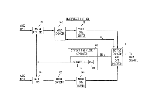
Specifir~lly, multiplexer unit 100, shown in FIG. 1 in simplified form,
includes in the video channel insert PTS, DTS unit 101, video encoder 102 and
video data buffer 103. The audio channel inr,l~ldes insert PTS unit 104, audio
20 encoder 105 and audio data buffer 106. Data from video data buffer 103 and audio
data buffer 106 are supplied to ~y~;lllS encoder and SCR inserter 110. Systems time
clock g~nel~lor 112 incl~ldes oscillator 114 and output counter 115. The output of
counter 115 is the STC value which is supplied to insert PTS, STS unit 101, insert
PTS unit 104 and ~y~cllls encoder and SCR inserter 110. It is noted that according
25 to the MPEG specifir~tinns~ the frequency for oscill~tor 114 shall be 90 kHz + 50
ppm. Ad-lition~lly, the frequency drift of oscill~tc?r 114 shall not exceed 250
mic~h.,.~/second. In this embodiment, counter 115 supplies a 33-bit STC value asan output that is inclr~ n~e-l once for each pulse supplied from oscill~t< rll4.The video input data is first supplied to insert PTS, DTS unit 101 which
30 inserts ~,se.~al;on Time Stamps (PTS) on some or all of the image l~,pl~,sent~tions,
i.e., picture frames. If a PTS is inserted on a non-Bidirectionally Predicted Image
Represent~fiQn (nonB-picture), then a Decoding Time Stamp (DTS) must also be
inserted. For these image ~ ,sentations, PTS exceeds DTS (in picture periods) byone plus the number of bidirectional image l~;pl~senta~ions to be encoded. The
35 resulting "time stamped" video data then passes to video encoder 102 where it is
encoded in known fashion. In turn, the encoded video data is supplied to video data
20973~
buffer 103 to await tr~n~mi~sion via :iy~enlS en~oder and SCR inserter 110.
The input audio is in the form of so-called Audio Access Units (AAU),
which are supplied to insert PTS unit 104 where PTS values are inserted on some or
all of the AAUs. Th~leaf~r, the AAUs are supplied to audio encoder 105 where
5 they are digitally encoded in well-known fashion and, thereafter, supplied to audio
data buffer 106 to await tr~n~mi~ion via s~lcms encoder and SCR inserter 110.
The PTS/DTSs are employed to control the decoding and displaying of
the audio and video data, in accordance with an aspect of the invention, in
dem--ltiplexer unit 200 (FIG. 2). The decoding and displaying in response to the10 PTS/DTSs are such as to n~Ai~lAin synchronism and to avoid overflow and underflow
of data buffers in demllltiplexer unit 200. Typically, the PTS/DTS values inserted by
units 101 and 104 are equal to some constant value plus the in~lA--I;1neous STC
values from systems clock gene~atol 112.
Systems encoder and SCR inserter 110 forms packs and packets of data
15 and supplies them asynch~ ously to a data co~ atiQn~ sh~nnel Packs include
packets from a plurality of video and audio encoders (not shown). Pack headers also
contain SCR values that are the in~t~nt~nçous values of STC from systems time
clock generator 112. According to MPEG specifi~ation~, packs must be tr~n~mittedat least every 0.7 second~ Additionally, the MPEG specifi~ti- n~ assume that the20 channel data rate is constant for the duration of the pack.
The packets in a pack contain video or audio data with the PTS/DTS
values, if any, moved to the packet header. Hence, for situations of more than one
PTS/DTS per packet, all except the first are discarded.
Ri is a re~ ;se..~tiQn of the number of bits being tr~n~mitted to the data
25 channel during the coding of image leplese-ltation (picture) i. For a current image
lep~ ion being tr~n~mitted, systems encoder and SCR inserter 110 supplies to
video cl-~ode~ 102 the actual number of bits being tr~n~mitted For future image
sen~lions, video encoder 102 supplies to systems encoder and SCR inserter
110 sllgg~st~d values for the number of bits to be tr~n~mitte~l for each image
30 I~;present~l;on Systems encoder and SCR inserter 110 then chooses the actual
values according to prescribed principles which are known (see, for example, ourarticle entitled "Constraints on Variable Bit-Rate Video for ATM Nelwol~s",
Document #AVC-56, CCITT STUDY GROUP XV WP XV/l, Experts Group for
ATM Video Coding, May 21, 1991).
_ 2~97~L9
FIG. 2 shows, in simplified block diagram form, details of dem-lltiplexer
unit 200. Specifir~lly, shown are system decoder and SCR extractor 201, which
supplies video il~fc....~tion to be decoded to video data buffer 202 where it is stored
awaiting display. Video data from buffer 202 is supplied to video display control
5 203 and, eventually, to video ~ecoder 204. Similarly, audio data is supplied from
systems decoder and SCR extractor 201 to audio data buffer 205 where it is stored
awaiting display. Audio data from buffer 205 is supplied to audio display control
206 and, eventually, to audio decoder 207. Systems decoder and SCR extractor 201also detects the received system clock reference (SCR) values and passes them to10 systems time clock ge~ alo 208 along with an enable signal which in-liriq~s when
there is a valid SCR value being received and a start up value.
Systems time clock genel~lol 208 is a phase locked loop inchlding
phase colllp~tor 210, filter 211, voltage controlled oscill~tor (VcO) 212 and output
counter 214. The enable signal from ~s decoder and SCR extractor 201 is
15 supplied to enable filter 211 when a valid SCR value is received. The start up value
is supplied to set counter 214 to the value of the initial SCR value being received, so
that the initial audio or video data in the packets of the initial received pack may
pr~,lly be displayed. The STC output from counter 214 is cOIllpalc;d in phase
colllpalator 210 to the received SCR value. Filter 211 smooths the dirr~ ces
20 SCR-STC and gell~lalt;s a control voltage which is used to control the frequency of
VCO 212.
In the absence of tr~n~mi~sion jitter delay, and as~ullling that the center
frequency of VCO 212 is close to that of the oscillator 114 in multiplexer unit 100
(FIG. 1), the control signal output of filter 212 will eventually stabili~ to a small,
25 nearly COIlSklllt value. If the frequency of oscill~tor 114 (E~IG. 1) drifts slightly
upward, then the SCR values will increase slightly, pro~ucing a corresponding
increase in the control voltage being supplied to VCO 212 which, in turn, increases
its fi~u~ . This, in turn, causes the STC values being supplied as an output from
~y~t~,llls time clock generator 208 to increase slightly, thus tracking the values of the
30 received SCR. Similarly, for a decrease in frequency of oscil1~or 114, the SCR and
STC values in demultiplexer unit 200 track each other by also decreasing.
The amount of smoothing provided by filter 211, i.e., the time duration
over which averaging occurs of the SCR-STC diLr~lellce signal, d~t~ ines how
fast VCO 212 can respond. A small amount of smoothing by filter 211 can cause a
35 rapid alignment of STC and SCR. However, if audio and video clocks were also
derived from VCO 212, such a rapid ~lipnm~nt could be de~;lll~,nlal to the audio and
_ 2~973 ~9
video quality. In such an in~t~nre~ ~ignifif~ntly more smrothing by filter 211 may
be n~ces~ry.
The gain of filter 211, or equivalently the input sensitivity of VCO 212,
also has an effect on the frequency stability of the output pulses being supplied to
5 counter 214. If the gain is large, then a small dirrcl~nce between SCR and STC will
cause a large frequency shift in the output of VCO 212. If the gain is too large, then
VCO 212 may never stabilize. If the gain is too small, stable operation could occur
even if SCR and STC were not close to each other.
The audio and video decoder timing is controlled via
10 P~csen~lion/Decode Time Stamps (PTStDTS) that are, as in~ t~.~ above, includcd
in the le.pc.-live audio or video data. ~ssumin~ PTSs occur on every image
fep.~;~n~;on the DTS (PTS, if no DTS) of the oldest image l~,plese .~ ;on storedin video data buffer 202 passes to video display control 203. Video display control
203 waits until the STC-Dj value increases to the value of the oldest DTS. It then
15 extracts the coded video data for the co l~;,poading image l~,~.cse .l~;Qn from video
data buffer 202 and passes it to video decoder 204 for deco~ For each video
image ..,p.~se~ ;on, input to decoder 204, the image l~ipl~ise ~ ;on is supplied as
the video output for display. The video output may be the same image
,senli~lion as the input (e.g., for B-pictures), or it may be a stored previously
20 decoded picture (e.g., for nonB-pictures).
If an image l~plesen~lion does not have a DTS, then video display
control 203 com~u~s an extr~rol~ted DTS value by simply adding the nomin~l
picture duration to the DTS of the previous image l~,~lcse,-t~tion It is ~sllmPd that
video decoder 204 always completes ~lecorling each image l~.esenl~l;Qn before the
25 next image l~plesent~tion is due to be decode-l When the oldest received (or
e~ ~l~d) audio PTS equals STC-Dj, then a next audio access unit in audio data
buffer 205 is supplied via audio display control 206 to audio decoder 207. The
audio is imme~i~tely passed as the audio output corresponding to the video
output to be displayed.
Details of the video and audio display controls are shown in FIG. 3 and
described below.
If there is substantial transmi~sion jitter delay, then dem~lltiplexer 200
may not operate correctly. This results because filter 211 of sy~tellls time clock
generator 208 must average over a much longer time interval than in a jitter free
35 situation. However, even if this is the case, a more serious problem is that the data
arrival times may be considerably different than was assumed in multiplexer 100
20g~3~ '~
- 7 -
(FIG. 1). When such an occullcince happens, there is a possibility of overflow or
und~lllo. ~ of the video and/or audio data buffers in demultiplexer 200.
Overflow of the data buffers can be readily avoided by increasing the
buffer si~s beyond what was ~sllmed by the encoder in multiplexer 100.
5 Underflow of the data buffers can be alleviated by the ~d~lition of a jitter delay Dj,
which causes an extra u~cllmlll~tion of data in the data buffers prior to decoding.
The additional stored data provides insurance against nn-1erfll~w. In fact, if bounds
on jitter delay can be guaranteed, the possibility of underfiow of the data buffers can
be substantially elimin~te~ by choosing sufficiently large buffers and a sufficiently
10 large value for Dj. This value of jitter delay Dj is then algebraically combined in
subtractor 216 with STC to form STC-Dj. The amount of the delay for MPEG is
given by Dj/90000 seconds. Then, the STC-Dj value is supplied to be utili~d in
video display control 203 and audio display control 206 as described below.
Dynamic tracking of jitter delay for the channel is realized by
15 employing co,~ule jitter delay unit 217 which dyn~mir~lly generates jitter delay
value Dj. The resulting dyn~mir~lly obtained value of Dj is supplied to a negative
input of subtractor 216 to obtain the value STC-Dj. To subst~nti~lly elimin~te data
buffer underflow, it is only necess~ry to insure that Dj is sufficiently large. Data
buffer underflow may occur if data is late in arriving, i.e., STC>SCR. Thus, a
20 conservative choice of Dj is the largest measured value of STC-SCR. In actualoperation, Dj is very slowly increased to the desired value without much effect on
audio and video quality.
In this embo liment~ the in~t~nt~n~ous fullness of video data buffer 202
is used to mrdul~t~ the value of jitter delay Dj. To this end, the fullness value of
25 video data buffer 202 is supplied to com~u~ jitter delay unit 217 along with the
SCR- STC value output from phase colllp~ator 210.
The colll~ute jitter delay process is illu~llated in the flow chart of FIG.
4. S~ lly, at start of the process step 401 initi~li7Ps the Dj value to a nomin~l
eAl~cb!~d jitter delay value. Step 402 then reads the fullness of video data buffer 202.
30 Step 403 tests to dele,ll~ine if the fullness value of video data buffer 202 is too large,
infli~ ting too much jitter delay. If the test result in step 403 is YES, step 404 causes
the value of Dj to be de~l~...f nled Th~ idrt.,~, control is passed to step 405. If the
test result in step 403 is NO, step 406 tests to determine if the fullness of video data
buffer 202 is too small. If the test result in step 406 is YES, step 407 causes the
35 value of Dj to be inc~ enled. Thereafter, control is passed to step 405. If the test
result in step 406 is NO, step 405 reads the value of SCR-STC from phase
2~97~
compa~o~ 210. Step 408 causes the sign of the value obtained in step 405 to be
ch~nge~l to obtain STC-SCR. Then, step 409 tests to detelllulle if the value of Djis
less than the value of STC-SCR. If the test result in step 409 is YES, step 410
in~e.l~llts the value of Dj. If the test result in step 409 is NO, control is returned to
5 step 402.
The alllUUlltS of the inclcll.ellts and dew~ ellls in the process of FIG. 4
depend on how fast an adaptation process is desired and upon how much stability is
required in the audio and video outputs. Such det~rmin~ti-n~ are left to be chosen
by the imple...f ..IO~ of the system.
FIG. 3 shows, in simplified block diagram form, details of a display
control unit which may be employed for either video display control 203 or audiodisplay control 206. It is noted that for audio display control 206 only PTS values
are employed. Specifically shown is depacketizer and DTS (PTS) extractor 301
which strips off packet headers and detects the presence of DTS and/or PTS. (The15 first packet received is required to contain a PTS.) If PTSIDTS is detected (set
DTS=PTS if no DTS), then switch 302 is set to the A position via a signal from
depacketizer and DTS (PTS) exLIaclol 301, and the DTS value is supplied to the Ainput of switch 302. In turn, the supplied DTS value is supplied as an output byswitch 302 as DTSl to DTS (PTS) register 303.
After stripping off packet headers, depacketizer and DTS (PTS)
extractor 301 passes the Ic.~ining packet data upon request to plese .L~Iion unit
(PU) detector 304. For video display control 203, a PU is an image lc~-~,se.~t~l;ûn
(i.e., picture). For audio display control 206, a PU is an Audio Access Unit (AAU).
At the start of every first PU (and no others), p.cs~ -t~l;on unit ~etector 304 outputs a
25 clock pulse that clocks DTS (PTS) register 303, thus causing its input DTSl to be
read, stored and then supplied as an output as DTS2 to subtractor 305 and adder 306.
Then, p~s~ nt~ t;OI~ unit clet~ctor 304 waits.
STC - Dj values are supplied to SUbL a~ r 305, where they are
COIllpdl~l with the stored DTS2 values. The resuldng dif~lcnce STC-Dj-DTS2
30 is supplied to zero ~ete~tor 307. When STC- Dj increases to a value equal to DTS2,
enable next PU signal is supplied as an output to plesentatiûn unit detector 304 and
the set B input to switch 302. This allows the next PU to be passed to the decoder.
For video display control 203, upon receiving this enable next PU signal present~tion
unit detector 304 transfers the data for the next PU to video decoder 204. Similarly,
35 for audio display control 206, the enable next PU signal causes p.eserltadon unit
detector 304 to transfer the data for the next PU to audio decoder 207. As indir~te-l,
20973Ji~
,.,
the enable next PU signal also causes switch 302 to be set to the B position. Ifduring the output of the PU depac~ti7~r and DTS (PTS) extractor 301 detects a
PTS/DTS, it sets switch 302 to the A position as before. However, if no PTS/DTS is
detected, switch 302 remains in the B position.
At the end of a PU data transfer by ~l~sel-t~tion unit detector 304, it
outputs a clock pulse to the clock input of DTS (PTS) register 303, as before. If a
new DTS value has arrived, it is read, as before, from the A input of switch 302 and
supplied as a DTSl value to register 303 and appears as a DTS output value from
register 303. However, if no new DTS value has arrived, then switch 302 still
10 remains in the B position. In this sit~1ation, an extrapolated DTS value is supplied
from adder 306 and is supplied as a new DTSl value to register 303 and appears at
an output thereof as DTS2. This extrapolated DTS value is obtained by adding viaadder 306 a constant nominal picture duration value in units of STC to the previous
DTS2 value. For example, if the nomin~l picture frequency is 29.97 Hz and the STC
15 frequency is 90 kHz, then constant is 3003.
P~sell~ion unit detector 304 then waits until STC-Dj increases to this
new value of DTS2, whereupon it receives an enable next PU signal (pulse) from
zero detector 307, thus repeating the data output cycle.
In critical, high quality application~ le.luiliilg a very stable video timing,
20 the stability of ~y~lellls time clock generator 208 may not be sllfficient to acquire the
desired quality level. For example, MPEG specifications call for the STC stability of
+ 50ppm while the industry standard for the tran~mi~sion video clock stability is +
3ppm. Consequently an arrangement of enh~ncing the video timing and
demllltirlexer unit 200is nçeded
To this end, FIG. S shows in simplified block diagram form, a time base
correction circuit that can be employed in place of zero detector 307 in FIG. 3 to
reali~ the desired quality of the video timing. Thus, as shown in FIG. 5, a timing
error signal STC-Dj-DTS2 is supplied via switch 501, filter 502 and clipper 503
to voltage control oscillator (VCO) 504. F.lem~nt~ 501 through 504 form an
30 ad-lition~l phase lock loop. VCO 504 supplies as an output a train of short pulses at
a nearly constant frequency. These output pulses are the enable next PU signals
supplied to present~tion unit detector 304 (~;IG. 3) and are also supplied to switch
501.
VCO 504 has a very stable center frequency confolll~illg to Video
35 Industrial Standards, e.g., 20.9Hz. Moreover, the frequency variation of VCO 504 is
limi~d, for example, + 3ppm during normal operation, by having its input control
~ 20973~
- 10-
voltage clipped to some small range by clipper 503. During startup of the system, it
may be desirable to provide for a faster synchroni7~tion by increasing the allowable
control voltage range. This is reali_ed by supplying a startup signal to clipper 503 to
allow for the wider voltage control range. As infiir~ted above, the enable next PU
5 signals (pulses) from VCO 504 are also employed to enable switch 501. Each such
enable next PU signal causes switch 501 to close, thereby allowing the inst~nt~neous
timing error signal input to be supplied to filter 502. Filter 502 averages the sampled
timing error signals, typically over some time window, and passes the results toclipper 503. Judicious choices of filter duration and gain determine the stability and
10 tracking rate of the phase lock loop of the time base c~~ or shown in FIG. 5.