Note: Descriptions are shown in the official language in which they were submitted.
2097353
ELECTRIC POWER CONVERTER
BACKGROUND OF THE INVENTION
The present invention relates to an electric power
converter for DC power transmission and frequency conversion
and particularly relates to a high-voltage large-capacity
electric power converter having a structure in which a
plurality of self quenching type switching elements per one
arm are connected in series.
With respect to gate electric sources adapted to
switching elements for driving a high-voltage large-capacity
electric power converter of the type having a structure in
which a plurality of semiconductor switching elements are
connected in series, there is a method in which insulation
transformers are series-connected from the ground side so
that respective gate drive circuits are supplied with
electric power from the secondary side of the transformers
as described in Japanese Utility Model JP-Y 2-31909
published August 29, 1990. Further, there is a method in
which a gate power source is obtained from the potential of
a main circuit in an apparatus using a thyristor as
described in Japanese Patent Publication Specification
JP-B 53-40860 published October 30, 1978. As another
method, there is a method in which a gate power source is
obtained from a main circuit through a current transformer
on the basis of a snubber circuit current as described in
Japanese Patent Laid Open Specifications JP-A 55-32449 and
JP-A 63-124777 which were laid-open on March 7, 1980 and
May 28, 1988, respectively.
.,
20973 ~3
However, for example, in a high-voltage
large-capacity electric power converter for DC power
transmission and frequency conversion as used in an
electric power system, for example, the value of DC
voltage reaches 125 kV. In the case where a 4.5 kV-grade
large-capacity gate turn-off thyristor (hereinafter
referred to as "GTO") is used as a self quenching type
semiconductor element, the number of series-connected
GTOs approaches 100 per one arm. Accordingly, in the
case where an electric source for each of gate drive
circuits for driving the GTOs is to be obtained from the
series-connected insulation transformers, the capacity of
an insulation transformer locted in the lowermost stage
from the ground side becomes a multiple of a capacity
corresponding to the number of switching elements or
corresponding to the number of modules each constituted
by a plurality of series-connected switching elements
so that apparatus size becomes large compared with the
capacity of an insulation transformer located in the
uppermost stage. In a method in which insulation
transformers are provided correspondingly to respective
potential values, the transformers can be provided so
as to be equal in capacity but insulation between the
primary winding (ground side) and the secondary winding
(apparatus side) cannot be made easily. Further, gate
drive electric power for a thyristor is required only at
the time of turning-on thereof while gate drive electric
2~973~ .3
power for a GTO is required both at the time of turning-
on and at the time of turning-off. As the GTO device
capacity increases or as the carrier frequency of the
apparatus increases, the drive electric power increases.
S For example, in the case of the above-mentioned
high-voltage large-capacity electric power converter,
if electric power required for the gate of a 4.5 kV-3
kA-grade GTO is 200 W in the condition of 100 series-
connected GTOs per one arm, three-phase bridge connection
and carrier frequency of 500 Hz, the number of GTOs
becomes 600. Accordingly, gate drive electric power
required for the apparatus as a whole becomes 120 kW as
bulk power. Therefore, the method in which a gate
electric source is obtA~ne~ from a main circuit, as
described in the prior art, is considered. However,
in the case where a self quenching type semiconductor
switching element such as a GTO is to be driven, an idea
different from the idea required for the thyristor
is required so that it is necessary to apply an
inverse-bias voltage to the gate in order to prevent
maloperation before a voltage is applied to the main
circuit. As a method for obtAin;ng a gate electric
source under the consideration of these problems, nothing
has been described specifically.
SUMMARY OF THE lNV ~:N~l~IoN
An object of the present invention is to
- 2ng73 ' 3
provide a high-voltage large-capacity electric power
converter constituted by a plurality of self quenching
type semiconductor switching elements connected in
series, in which high efficiency of the converter can be
attained through reduction in size and saving of electric
power in a gate driver for driving the semiconductor
switching elements.
The foregoing object of the invention is
attained by an electric power converter comprising a
plurality of reactors, a plurality of self quenching type
switching elements, the reactors and switching elements
being series-connected per one arm, and surge-absorbing
snubber circuits connected in parallel to the switching
elements respectively, the switching circuits being
driven by gate drive circuits connected to respective
gates of the switching elements to thereby convert a DC
voltage to an AC voltage or convert an AC voltage to a DC
voltage, wherein the electric power converter further
comprises means for recovering energy accumulated on the
rectors and the snubber circuits, meansfor generating a
DC source for supplying electric power to each of the
gate drive circuits on the basis of the recovered energy,
and a sub power source connected in parallel to the DC
source and constituted by a battery for supplying
electric power to each of the gate drive circuits.
An electric source for each of the gate
drive circuits for the plurality of series-connected
20~3~' 3
semiconductor switching elements is generated from energy
accumulated on the reactor and the snubber circuit to
thereby reduce the potential difference between the
electric source and the semiconductor switching element.
Accordingly, not only the insulating process in the gate
driver including the electric source can be lightened
but reduction in size can be attained. Further, in the
above-mentioned method, there is no necessity of supplyin
gelectric power from the outside. Accordingly, not only
greater reduction in size of the gate drive circuit can
be attained but high efficiency as a whole of the
electric power converter can be attained. Further,
because the sub power source supplies electric power to
the gate drive circuit only when the DC voltage is not
established at the time of the starting-up of the
electric power converter, the capacity thereof can be
selected to be small. In the case where a secondary
battery is used as the sub power source, the battery is
charged by the above-mentioned DC source at the time of
constant operation. There arises an effect that no
special electric charger is required.
BRIEF DESCRIPTION OF THE DRAWINGS
Fig. 1 is a configuration diagram of a main
circuit of an electric power converter showing an
embodiment of the present invention;
Fig. 2 shows a regenerative circuit in the
20973~ 3
embodiment of the present invention;
Fig. 3 shows a gate drive circuit in the
embodiment of the present invention;
Fig. 4 is a configuration diagram of part of a
main circuit of an electric power converter showing
another embodiment of the present invention;
Fig. 5 is a configuration diagram of part of a
main circuit of an electric power converter showing a
further embodiment of the present invention;
Fig. 6 is a configuration diagram of part of a
main circuit of an electric power converter showing a
further embodiment of the present invention;
Fig. 7 is a graph for explaining the operation
of Fig. 6;
Fig. 8 is a configuration diagram of part of a
main circuit of an electric power converter showing a
further embodiment of the present invention;
Fig. 9 is a configuration diagram of part of a
main circuit of an electric power converter showing a
further embodiment of the present invention;
Fig. 10 is a configuration diagram of part of
a main circuit of an electric power converter showing a
further embodiment of the present invention;
Fig. 11 is a configuration diagram of part of
a main circuit of an electric power converter showing a
further embodiment of the present invention; and
Fig. 12 is a configuration diagram of part of
2~973~
a main circuit of an electric power converter showing a
further embodiment of the present invention.
DESCRIPTION OF THE PREFERRED EMBODIMENTS
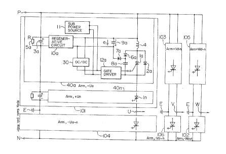
Fig. l shows a main circuit configuration of
an electric power converter (popularly called "inverter")
for converting AC power into ~C power, to which an
embodiment of the present invention is applied. In Fig.
1, a three-phase voltage type inverter is shown as an
example. A plurality of self quenching type semi-
conductor switching elements are series-connected to each
of six arms 101-106. In this drawing, GTO is used as an
example of the semiconductor switching element. In the
drawing, P represents a positive side terminal of the
inverter, N represents a negative side terminal of the
inverter, and U, V and W represent three-phase AC
terminAls connected to load sides respectively. A
plurality of smoothing capacitors 3a are series-connected
between the terminals P and N. An intermediate point E
of the connection is connected to the ground.
The internal structure of each arm will be
described below on the basis of the U-phase positive side
arm 101 taken as an example because the arms 101-106 are
the same in structure. A number n of GTOs la-ln are
series-connected per one arm. The reference numeral
40a designates a circuit which includes a GTO la and
attendant peripheral circuits. Circuits equivalent to
-
2~3 ~3 ~ 3
the circuit 4Oa are provided correspondingly to the
number of GTOs. That is, circuits 40a-40n are provided.
The structure of the circuit 40a which is one of the
circuits 40a-40n will be described below. An anode
reactor 4 is series-connected to the GTO la and for
suppressing the ascension rate and overcurrent state of
electric current flowing in the GTO. Further, a snubber
circuit constituted by a series circuit of a diode 6a and
a capacitor 8a, and a feedback diode 2a are connected in
parallel to the GTO. The snubber circuit is provided for
suppressing the ascension rate and overvoltage state of
voltage applied to the GTO. A junction between the diode
6a and the capacitor 8a in the snubber circuit and an end
of a capacitor 9a are connected to each other through a
diode 7a with polarity shown in the drawing. Opposite
ends of the capacitor 9a are connected to not only the
input side of a regenerative circuit 10a but the input
side of a DC-DC converter 30 which receives a
predetermined range of DC input voltages and outputs a
constant DC voltage. The output side of the converter 30
is connected to the input side of a gate drive circuit
12a. The input side voltage of the regenerative circuit
10a is generally controlled by the regenerative circuit
10a so as to be kept substantially in a predetermined DC
voltage value el. Further, a sub power source 11 such as
a battery is connected to the input side of the gate
drive circuit 12a. The output side of the regenerative
--- 2~S-~3~
circuit lOa is connected to opposite ends of the
smoothing capacitor 3a. The reference numeral 5a
designates a voltage dividing resistor for dividing a
voltage equally.
Fig. 2 shows the detail of the regenerative
circuit lOa in the embodiment of the present invention
shown in Fig. 1. The regenerative circuit is a circuit
for regenerating energy to a PN side DC source. The
circuit shown in this drawing is a known circuit which
is called "DC-DC converter". In this embodiment, this
circuit is shown as a series resonance type circuit.
Briefly describing the operation of this circuit, when
semiconductor switches 13a and 13b connected in parallel
to feedback diodes 14a and 14b are turned on and off
alternately with a capacitor 9a as a power source
(voltage el), a resonance current (AC current) flows in
the primary side of a potential transformer 16a through
a capacitor 17a and a reactor 18a. The current is
rectified by diodes 15a and 15b on the secondary side of
the potential transformer 16a, so that the rectified
current is regenerated to the smoothing capacitor 3a.
Fig. 3 shows the detail of the gate drive
circuit 12a in the embodiment of the present invention
shown in Fig. 1. This circuit is also a kind of DC-DC
converter. The primary winding side of a potential
transformer 16b is formed so as to be of a push-pull
type. By turning on and off semiconductor switches 13c
- 2~1973~
and 13d alternately while using an input supplied from
the converter 30 as an electric source, a high-frequency
AC voltage is generated. Voltages generated on the basis
of the voltage are rectified by diodes 15c-15f on the
secondary side of the potential transformer 16b and
charged in an on-source capacitor 29a and an off-source
capacitor 29b respectively. On the basis of a signal
from a control circuit not shown, a semiconductor switch
13e is turned on in the case of an on-gate signal or a
semiconductor switch 13f is turned on in the case of an
off-gate signal so that a gate signal is transmitted to
the GTO.
The operation of the embodiment of the present
invention will be described below. First, in the state
in which the GTO la is off, the capacitor 8a in the
snubber circuit is charged with a voltage obtA i ne~ by
dividing the DC voltage between the terminals P and N by
the number in series connection of GTOs. When the GTO la
is turned on, the energy accumulated on the capacitor 8a
is supplied to the capacitor 9a through a closed circuit
of capacitor 8a - diode 7a - capacitor 9a (the primary
side of the regenerative circuit 10a) - anode reactor 4 -
GTO la so that the capacitor 9a is charged. The charge
energy is regenerated to the source-side smoothing
capacitor 3a through the regenerative circuit 10a till
the voltage of the capacitor 9a reaches a predet~rri ne~
value.
-- 10 --
. 2as-~3s3
When the GTO la is then turned off, the energy
accumulated on the anode reactor 4 is supplied to the
capacitor 8a so that the capacitor 8a is charged. In the
case where the total capacitor voltage in the snubber
circuit per one arm exceeds the DC voltage inputted to
the inverter, the energy is fed to the regenerative
circuit through a closed circuit of anode reactor 4-
diode 6a - diode 7a - capacitor 9a. That is, energy
accumulated on the anode reactor and the snubber circuit
is fed to the regenerative circuit whenever the GTO is
turned on and off. Accordingly, part of the energy is
fetched in the input of the gate drive circuit 12a as
shown in the drawing so as to be used as gate drive power
for driving the GTO. According to a trial, electric
power required for gate driving is not larger than
several ~ of the energy accumulated on the anode reactor
and the snubber circuit. As described above, when the
electric power converter is in operation, gate drive
power for driving the GTO can be supplied sufficiently
from the main circuit. There is however the necessity
of consideration of the following point at the time of
starting-up of the electric power converter. That is,
though an electric source voltage must be established in
order to start up the inverter, an overcurrent may flow
in the GTO because of ignition by mistake when an
electric source voltage is supplied to the gate terminal
of the GTO which has been not supplied with an inverted
- -- 2~37~2 ~
bias voltage. Further, because there is no gate power
obtained from the main circuit at the initial stage of
the starting-up, gate drive electric power enough for
turning on and off the GTO is required in a period of
several cycles till constant gate power is supplied.
Therefore, as shown in Fig. 1, a sub power source 11 is
connected to the input side of the gate drive circuit
12a. As the power source 11, a secondary battery is
~sed. The secondary battery is preliminarily charged
before the starting-up of the electric power converter,
so that the battery is used as a power source for
generating the above-mentioned inverted bias voltage and
gate drive power at the initial stage of the starting-up
and as a power source for controlling the regenerative
circuit lOa and the gate drive circuit 12a. Because the
electric power is sufficiently smaller than the gate
power required for turning on and off the GTO constantly,
the secondary battery can be used sufficiently.
Alternatively, a primary battery such as a solar cell may
be used as the sub power source 11. In the case of a
solar cell, the battery does not need charging because it
always absorbs peripheral light energy and converts the
light energy into electric power. Further, if the solar
cell and the above-mentioned secondary battery are used
in combination, charging of the secondary battery before
the starting-up is not required. Alternatively, an
insulation transformer may be series-connected from the
-
2 ~ 9 7 3 ~ ~
ground side so that secondary side outputs of the
insulation transformer having respective potential values
are rectified to be used as sub power sources. In this
case, there arises a problem in insulation between
the primary and secondary sides of the insulation
transformer, but the capacity of the transformer can be
reduced so that the size thereof can be reduced because
there is no necessity of constantly supplying gate drive
power for turning on and off the GTO.
As described above, in this embodiment, when
energy generated in the ~ain circuit portion of the anode
reactor and the snubber circuit is regenerated to the
power source by the regenerative circuit in a period of
operation of the converter, part of the energy is used as
gate drive power. Accordingly, there is no necessity of
supplying electric power from the outside, so that high
efficiency as a whole of the electric powerconverter can
be attained.
Further, a gate drive power source is
generated from the main circuit portion of the anode
reactor and the snubber circuit, so that potential
difference between the power source and the gate of the
GTO is reduced. Accordingly, an insulating process in
the gate driver including the power source can be
reduced, so that reduction of size can be attained.
Fig. 4 shows the structure of part of the main
circuit according to another embodiment of the present
2~3~3-, ~
invention. One unit constituted by a plurality of GTOs
being series-connected and attendant parts, necessary on
circuitry, being connected to the GTOs is now referred to
as "module". Because the number of series-connected GTOs
is large in practical use of a large-capacity converter,
a necessary number of above-mentioned modules are
series-connected in accordance with the rated voltage.
Although Fig. 4 shows the case where three GTOs are
series-connected in a circuit 50a of one module, the
number of series-connected GTOs is not limited to the
specific value and can be determined freely. In this
embodiment, the number of series-connected modules is
selected to be m, and a circuit 5Om is the m-th module
and has the same circuit structure as the circuit 50a.
That is, in the circuit 50a, feedback diodes 2a-2c,
diodes 6a-6c of a snubber circuit and capacitors 8a-8c of
the snubber circuit are connected in parallel to the GTOs
la-lc. Energy accumulated on the capacitors 8a-8c of
the snubber circuit is fed to a capacitor 9a and to a
regenerative circuit 10a through diodes 7a-7c. The
operation in Fig. 4 is the same as that in Fig. 1, and
the description thereof will be omitted. In a gate drive
circuit 12a', a plurality of secondary winding sets are
provided by a potential transformer 16b', and respective
secondary side outputs are insulated electrically so that
gate electric power is transmitted. The gate drive
circuit 12a' is substantially equivalent to the gate
- 14 -
20g ~ 3 3
drive circuit 12a except that the plurality of secondary
winding sets are provided in the gate drive circuit 12a'.
In this embodiment, only one sub power source can be
provided to thereby simplify the circuit structure.
Although the embodiments in Figs. 1 and 4 show the
circuit structure in which energy of the anode reactor
and the snubber circuit for the GTOs is processed by the
regenerative circuit, it is to be understood that the
invention is not limited thereto and that the invention
can be applied to another circuit structure in which
energy accumulated on only the anode reactor circuit or
only the snubber circuit for the GTOs is processed by the
regenerative circuit.
Fig. 5 shows the structure of part of the main
circuit according to a further embodiment of the present
invention. In the drawing, there is shown the case where
the number of series-connected GTOs is one. In each of
Figs. 5 and 2, like numerals refer to like parts. In
Fig. 5, a current transformer l9a is provided in the
input side of the regenerative circuit lOa. The output
of the current transformer l9a is full-wave-rectified by
a diode bridge 20a and supplied to a capacitor 2la so
that the capacitor 2la is charged. The charge voltage of
the capacitor 2la is used as an input to the gate drive
circuit 12a. Further, a sub power source 11 is connected
to the input side of the gate drive circuit 12a. With
respect to the operation in this structure, an input-side
2as7~
alternating current generated by alternatively turning
on and off semiconductor switches 13a and 13b of the
regenerative circuit lOa is picked out through the
current transformer l9a so that the electric power is
used as gate power. That is, this embodiment shows the
case where current is used as a gate power source, while
the embodiment of Fig. 1 shows the case where voltage is
used as a gate power source.
In this embodiment, a current transformer
which is relatively easy in insulation compared with a
potential transformer is used as a gate power pick-out
means, so that there arises an advantage in production of
parts. Although this embodiment has been described upon
the case where the number of series-connected GTOs is
one, the invention can be applied to thecase where a
plurality of series-connected GTOs are provided as one
module unit. In this case, the circuit structure can be
more simplified because one sub power source 11 can be
provided correspondingly to one module as described
above.
Fig. 6 shows the structure of part of the main
circuit according to a further embodiment of the present
invention. A snubber circuit is generally formed by
connecting a discharge resistor in parallel to a series
circuit constituted by a diode and a capacitor as shown
in the drawing. In this embodiment, a potential
transformer 16c is series-connected to the resistor 22a
- 16 -
21~973~ 3
at one terminal, and the other ter~i n~ 1 of the potential
transformer 16c is connected to a junction of a diode
6a and a capacitor 8a. The output of the potential
transformer 16c is rectified by a diode lSg and supplied
to a capacitor l9c so that the capacitor l9c is charged.
The charge voltage of the capacitor l9c is used as an
input to the gate drive circuit 12a. The drive output of
the circuit 12a is connectd to the gate of the GTO la.
The operation in this structure will be described below.
A voltage is supplied to the input-side winding of the
potential transformer 16c only when the GTO is turned on
to thereby discharge the capacitor 8a, because it is
bypassed by the diode 6a when the GTO is turned off.
Referring to Fig. 7, this fact will be
described. This drawing is a B-H curve graph of an iron
core of the potential transformer 16c. In this drawing,
when only one-side polarity is excited, flux density can
but be used within a range ~Bo2 between r-ximll~ flux
density Bs and residual flux density Br represented by
point h, and the iron core is saturated i~e~iately so
that sufficient electric power cannot be taken outof the
potential transformer. Therefore, when a magnetic field
inverse-biased by ~Hl is applied to the iron core so as
to be shifted to point i, flux density can be used within
a range ~Bo1 so that larger electric power can be
supplied from the potential transformer. For this
reason, in this embodiment, the potential transformer 16c
2~7~'~ 3
uses an iron core in which a material for inverse-biasing
the magnetic field is incorporated. In this embodiment,
the circuit structure can be simplified because gate
electric power can be obtained from a conventional
snubber circuit even in the case where there is no
regenerative circuit provided specially. Further, larger
electric power can be obtained because a potential
transformer provided with an iron core having a magnetic
field inverse-biasing function is used. Although this
embodiment has been described upon the case where a
discharge resistor is provided, the invention can be
applied to the case where there is no discharge resistor
provided.
Fig. 8 shows the structure of part of the main
circuit according to a further embodiment of the present
invention. This drawing shows the case where the number
of series-connected GTOs is one. This embodiment shows
the case where a current transformer is used for picking
out energy of the snubber circuit, while the embodiment
of Fig. 6 shows the case where a potential transformer is
used. That is, a current transformer l9b is inserted
into a conductor connected to the capacitor 8a of the
snubber circuit for the GTO la. The output of the
current transformer l9b is full-wave-rectified by a diode
bridge 20b and supplied to a capacitor 21b so that the
capacitor 2lb is charged. The charge voltage of the
capacitor 2lb is used as an input to the gate drive
- 18 -
2~!~7;3~ 3
circuit 12a. The output of the circuit 12a is connected
to the gate of the GTO la. In this embodiment, there
arises an advantage in production of parts because a
current transformer which is relatively easy in
electrical insulation compared with the potential
transformer is used as a gate power pick-out means as
described above. Further, because currents inverted in
polarity to each other flow in the current transformer
correspondingly to the turn,ing-on and turning-off of
the GTO, setting and resetting of the iron core can be
performed so that the size of the current transformer can
be reduced.
Fig. 9 shows the structure of part of the main
circuit according to a further embodiment of the present
invention. This embodiment shows the case where a
current transformer is used for picking out energy of the
snubber circuit in the same manner as in the embodiment
of Fig. 8 and where a plurality of GTOs are connected in
series. In the drawing, a circuit 50e shows the case of
a module constituted by three GTOs connected in series.
Circuits 40c-4Oe have the same circuit structure. In
this configuration, positive side terrin~ls al-a3 and
negative side terminals bl-b3 of diode bridge DC outputs
of the circuits 40c-40e are connected in parallel to a
capacitor 21c. The energy of the capacitor 21c is fed
to the respective gates of the GTOs la-lc through a gate
drive circuit 12a'.
-- 19 --
2~)973 ~ ~
In this embodiment, the circuit structure is
simplified because only one sub power source 11 can be
provided in the module, compared with the embodiment
shown in Fig. 8. Further, because current transformer
outputs from the respective GTOs are inputted in parallel
to the input-side capacitor of the gate drive circuit,
the input voltage of the gate drive circuit is kept
constant and accordingly the gate electric power is kept
constant compared with the case where gate power is
obtained individually from each of the GTOs. This is an
important point because the fact meant by this is that
partial charge voltages can be made even easily when the
GTOs are turned on and off in the case where the GTOs are
connected in series.
Fig. 10 shows the structure of part of the
main circuit according to a further embodiment of the
present invention. This embodiment is different from the
embodiment of Fig. 9 in that capacitors 2ld-2lf charged
through respective diode bridges are connected in series
so that the voltage between opposite terminals of the
series-connected capacitors is used as an input to the
gate drive circuit 12a'.
In this embodiment, not only the same effect
as in the embodiment of Fig. 9 is attained but the
following effect is attained. That is, the current
transformer picks out a current in the secondary side in
the winding ratio (ratio of current transformation) of a
_ 20 -
2 ~3 9 ~ 3 .~ 3
certain value so that the capacitors are charged.
Assuming now that the winding ratio of the primary side
to the secondary side is 1 : 5, then the primary side
voltage is 40 V when the secondary side voltage is 200 V.
Because this voltage is added to the anode-cathode
voltage of the GTO, the GTO needs durability against a
corresponding higher voltage. When current transformer
outputs are therefore arranged in parallel as shown in
this embodiment, a voltage value obtained by dividing the
secondary side voltage by the number of series-connected
GTOs ( in this embodiment, one third as much as the
secondary side voltage) is required in order to obtain
the same secondary side voltage as described above.
Accordingly, the durability against voltage, of the GTO
is lightened.
Fig. 11 shows the structure of part of the
main circuit according to a further embodiment of the
present invention. This embodiment shows the case where
a gate drive power source is obtained from a smoothing
capacitor correspondingly to one GTO. In this drawing,
smoothing capacitors 3a-3c are provided separately
correspondingly to respective GTOs. Resistors 5a-5c
connected in parallel to the smoothing capacitors 3a-3c
respectively are used for dividing a voltage, but there
is no necessity of providing the registers 5a-5c if the
partial charge voltages of the smoothing capacitors are
kept even.
- 21 -
2~73~. ~
Circuits 23a-23c have the same circuit
structure as described above.
In this embodiment, a DC source generated by
dividing a DC side DC voltage of the electric power
converter is used as an electric source for each of the
gate drive circuits for the above-mentioned series-
connected GTOs to thereby make it possible to reduce the
potential difference between the DC source and the GTO.
Accordingly, not only the insulating process in the gate
driver including the DC source can be lightened but
reduction in size can be attained. Further, because the
DC source is obtained from the smoothing capacitor used
as a DC input source for the inverter, there arises an
effect that electric power can be obt~;ne~ easily.
Although this embodiment shows the case where a gate
power source set is provided correspondingly to one GTO,
the invention can be applied to the case where one gate
power source set is provided correspondingly to a
plurality of GTOS connected in series. In this case,
the smoothing capacitor is divided correspondingly to the
number of units with the plurality of GTOS regarded as
one unit. By this division, there is provided an effect
that the circuit structure is simplified. Further, the
smoothing capacitor is not divided but a capacitor having
a smaller value than the smoothing capacitor may be
provided as a capacitor for a gate power source cor-
respondingly to one GTO or correspondingly to a plurality
209 73 ~ 3
of GTOs. In this case, there arises an effect that
production can be made more easily than the case where
a large-capacity smoothing capacitor is divided.
Fig. 12 shows the structure of part of the
main circuit according to a further embodiment of the
present invention. This embodiment shows the case where
a current flowing out of or into a smoothing capacitor 3
provided in the DC side of the inverter on the basis of
the operation of the inverter is picked out by a current
transformer 19e to thereby generate a gate drive power
source.
As described above, in this embodiment, a
current transformer which is relatively easy in
insulation compared with a potential transformer is used
as a gate power pick-out means, so that there arises
an advantage in production of parts. Although this
embodiment shows the case where a gate power source set
is provided correspondingly to one GTO, the invention can
be applied to the case where one gate power source set is
provided correspondingly to a plurality of GTOs connected
in series. In this case, there arises an effect that the
circuit structure is simplified.
As described above, according to the present
invention, an electric source for each of the gate drive
circuits for the plurality of series-connected semi-
conductor switching elements is generated from energy
accumulated on the reactor and the snubber circuit to
2G~7~
thereby el;~;nAte the necessity of supplying electric
power from the outside. Accordingly, high efficiency as
a whole of the electric power converter can be attained.
Furthermore, regardless of the gate drive power source,
the potential difference between the power source and the
switching element can be reduced. Accordingly, not only
the insulating process in the gate driver including the
power source can be lightened but reduction in size can
be attAine~.
Further, because the sub power source supplies
electric power to the gate drive circuit only at the time
of the starting-up of the electric power converter, the
capacity thereof can be selected to be small. In the
case where a secondary battery is used as the sub power
source, the battery is charged by the above-mentioned DC
source at the time of constant operation. There arises
an effect that no special electric charger is required.
- 24 -