Note: Descriptions are shown in the official language in which they were submitted.
20~73;~ ~
BATTERY FEED ClRCVIT
Technical Field
This invention relates to telecommunications.
Background and Problem
S Line circuits are used in telephone switching systems both to transmit
AC signals between the telephone line and the switching network of the system, and
to provide DC power to operate the station set. In order to properly match the
impedance of the telephone line and to provide sufficient DC current to power the
station set, switching systern line circuits are required to provide a terrnination which
10 has an AC impedance ~hat is somewhat larger than its I~C impedance. Typical
valulos for the AC and DC impedances are 600 ohms and 500 ohms respectively.
In a cornmonly used line circuit of the prior ar~ disclosed in Basic
Telephone Switching Systems, David Talley, 1979, line feed resistors are connected
in series with the pnmary windings of an AC coupling transformer. The line feed
15 resistors are chosen such that when their resistance values are added to the primaIy
winding resistance of the trans~ormer, the required DC impedance is achieved. The
required AC impedance is achieved by teIminating the transformer secondary
windings with the required impedance. However, since all the DC station set current
must flow through the transforrner primary windings in the switching system line20 circuit, the transformer is both large and expensive.
U. S. Patent 4,243,842 issued to W. D. Gibb on January 6, 1981,
discloses a line circuit where an additional flux cancellation winding substantially
reduces the DC current through the primary windings. The transformer is still not as
small and inexpensive as desired because of the additional winding and because
25 some of the flux is not cancelled and accordingly the DC current through the primary
windings is not reduced to zero. Further a required cu}rent sensing circuit and a
current source that are part of the Gibb circuit add to its cost.
V. S. Patent 4,476,350 issued to D. W. Aull et al. on October ~, 1984
discloses a line circuit which provides the required DC and AC termination
30 impedance without the need for a transformer. Accordingly, the size of the circuit is
substantially reduced. Although the solid state circuitry performs a number of
additional ~unctions, its cost is a significant disadvantage. In addition, the circuit
requires substantial prote- tion circuitry that further increases the cost.
In view of the foregoing, a need exists in the art for a line circuit that
35 provides specified DC and AC terrnination impedances with reduced cost.
~: .: , . :- . ,
: . , ~, ~
, .. -.: . .
: ,:: ; i
2~9733 ~
- 2 -
Solutiorl
This need is met and a technical advance is achieved in accordance with
the principles of the invention in a battery feed circuit where only a simple resistive
feed is required to provide DC current to the load, e.g., telephone line and station set,
5 because the part of the circuit which transmits and receives AC signals has an AC
impedance ~hat is negative. The circuit meets specified requirements for a n AC
termination impedance that is larger than the DC termination impedance because the
negative AC impedance is connected in parallel with the resistive feed. The circuit
achieves a substantial cost reduction with respect to prior art circuits 'oecause the DC
10 feed part of the circuit has only passive components and because the telephone line
is directly connected to only passive components in the AC part of the circuit,
thereby reducing the cost of protection circuitry required.
A circuit in accordance with the invention has line feed resistance
connecting a DC voltage source to an electrical load. A circuit, used for transmitting
lS AC signals to and from the load and having a negative AC impedance, is connected
in parallel with the line feed resistance.
Illustratively, the AC circuit has a substantially infinite DC impedance~
The magnitude of the negative AC impedance exceeds the magnitude of the
impedance of the DC line feed resistance. The negative AC impedance is achieved
20 by providing positive AC feedback to the load. The AC impedance of the overall
batte;y feed circuit is greater than the positive AC impedance of the line feed
resistanee. Consequently, the resulting parallel combination of negative and positive
AC impedances has a posidve AC impedance, making the circuit unconditionally
stable.
In a second embodiment, a transfolmer is used to couple the AC circuit
to the load. Again positive AC feedback is used to achieve a negatiYe AC
impedance. The transformer is small and inexpensive because substantially zero DC
current flows through the primary windings.
In a third embodiment, a digital signal processor processes digitized
30 signals to provide positive AC feedback to the load to obtain a negative AC
impedance.
In a further embodiment, line feed resistance connects a DC voltage
source to an electrical load. An AC circuit, used to transrnit AC signals to and from
the load and having a negative DC impedance, is connected in seAes with the line35 feed resistance.
.. : . .
. . . .
~(r~7~ ~
In this embodiment, the AC circuit has substantially zero AC
impedance. Ihe magnitude of the negative DC impedance is less than the magnitudeof the impedance of the line feed resistance.
Drawin~ Description
S FM. I is a block diagram of a circuit illustrating the principles of the
present invention;
FIG. 2 is a schematic diagram of a first battery feed circuit embodiment
in accordance with the invention;
FIG. 3 is a schematic diagram of a second battery feed circuit
10 embodiment in accordance with the invention;
FIG. 4 is a schematic diagrarn of a third battery feed circuit embodiment
in accordance with the invention; and
FIG. 5 is a block diagram of an alternative to the circuit of FIG. 1.
Detailed Description
FIG. 1 is a diagram of a circuit 10 used to illustrate principles of the
present invention. Two 250-ohm line feed resistors LFRl and LFR51 are used to
connect a DC voltage source -48V via tip and ring terminals T and R to an electrical
load comprising a telephone line and a station set. Typically, the re~quired DC
resistance of circuit 10 is 500 ohms and the required AC impedance is 6û0 ohms. To
20 achieve the 6~) ohms AC impedance, two impedances Z 1 and Zsl are connected in
parallel with the line feed resistors LFR1 and LFR51 respectively. Impedances Z
and Zsl each have a substantially infinite DC impedamce and a negative AC
impedance of -1500 ohms. As shown in FIG. 1, this results in an AC impedance forthe overall circuit of 6ûO ohms. Note the following: 1) the magnitudes of the
25 negative AC impedances Z I and Z 5l are grea~er than the corresponding resistance
values of line feed resistors LFR 1 and LFR5 1 respectively, and 2) the AC impedance
of the combination of LFR1 in parallel with Z 1 is greater than the positive AC
impedance of LFRl and the AC impedance of the combination of LFRSl in parallel
with Zsl is greater than the positive AC impedance of LFR51. The principles of
30 FIC;. 1 are applied in three embodiments of the invention--circuit 20 (FIG. 2), circuit
30 (FIG. 3), and circuit 40 (FIG. 4).
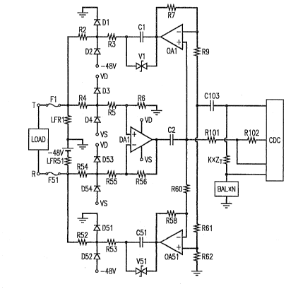
Batte~y feed circuit 20 (FIG. 23 is a first embodiment of ~he present
invention. The components in circuit 20 are detailed in Table 1.
. ". .,
,
2 ~ 9 7 2 .~, ~
_
LFRl,LFRS1 250Q R62 36.6kQ
R2,R52 1.75kQ Cl, CS1 0.47~,lf
R3,R53 2~0Q C2 4.7~1f
S R4,RS4 150kQ C103 1.0,uf
RS,RS5 50kQ DAl,OAl,OAS1 Motorola MC34074
R6,E~56 50kQ CDC Na~ional TP3054
R7 73.2kQ R101,R102 47kQ
RS8 93.2kQ BAL 600Q + 2.16~f
R9 20kQ k, N 100
R60 20kQ R61 20kQ
ZT ~oon
i
Table 1
It is typically required that circuit 20 present a 500 ohm DC termination impedance
and a 600 ohm AC termination impedance. As in cireuit 10, two 250 ohm line feed
resistors LFR1 and LFRSl are used to connect a source of potential -48V via tip and
ring tenninals T and R to an electrical load comprisirlg a telephone line and a station
20 set. A differential arnplifier DA 1 is used to transrnit AC signals from the load to a
coder/decoder (codec) CDC of a telephone switching system. Two operational
amplifiers OAl and OA51 transmit AC signals from codec CDC to the load~
Positive AC feedback is provided to the load by connecting the OlltpUt terminal of
arnplifier DA 1 via a capacitor C2 to the noninverting input terminal of amplifier
25 OA1 and to the inverting input terminal of arnplifier OA51. To verify that the AC
impedance connected across LFRSl is -1500 ohms, it is assumed that a 1~00 ohm
resistor is connected between ten~inal R and ground twith the load and resistor
LFRS 1 disconnected). Accordingly, the AC impedance between terminal R and
ground should be substantially infinite and the voltage gain around the lower loop of
30 circuit 20 (from terrninal R through amplifier DAl and back through amplifier OA51) should be 1.0 as shown in equation [1].
VOUt 2 ~ RS6 ~ ~ RS8 ~ ~ l.Sk
V,l, lR55+R54J lR60J ll.51c+R52+R53J
, ; - . - . . :;
:.. ,: .. . .
, , : .. ,.. ,,: , ,:,.... . ...
:: : ,. , .. .. ~
. ~ .. ....
,, , :,
.. . .. . . ..
: . . ~ . .
:., ~ , :, :
2~3~ ~
f SOk ~ ~ 93.2k ~ ~ l.Sk
l 50k+ 150k J l 20k J l 1. 5k+ 1.75k+ .25k J [ 1 ]
To verify that the AC impedance connected across LFRl is -150t3 ohms, it is
assumed that a 1500 ohm resistor is colmected between terrI.unal T and ground (with
the load and resistor LFRl disconnected). Accordingly, the combined AC
S impedance between terrninal T and ground should be substantially infinite and the
voltage gain around the upper loop of circuit 20 (~rom terminal T through amplifier
DAl and back through amplifier OAl) should be 1.0 as shown in equation [21.
Vout ~ R6 ~ ~ R7 ~ ~ 1.5k
V = 2x l RS+R-4 J x ll + R9 J x l 1 Sk R2 R3 J =
~ SOk~ lSOk ~ ~ ~Ok ~ [ 1-5k~ 1 75k+.25k ] [2]
10 The factor of 2 appears in equations [1] and [2] because the voltage input toarnplifier DAl is twice the ~ip to ground voltage or twice the ring to ground voltage.
The receive gain RGT from codec C~C to terrninal T is given by equation ~3].
RGT = ~ R9 ~ x ¦ 0.3k+R2+R3 ¦
73.2k ~x ~ 0-3k ~ _0.477 [3]
~ 20k J ~ 0.3k+ 1.75k+.25k
15 The same value is obtained for the receive gain RG R from codec CDC to terminal R
as given by equation [4].
RGR = ~ R62+R61 ¦ x ¦ R60 + l¦ x ! o 3k--- 5k R53 ¦ =
., , . -
' .,, ':', ' : ,, .
'
` ',, , ~' ' , : ;
2 ~3 ~ i 3; ~
36.6k ~ ~ 93-2k +11 ~ 0-3k l =o,477 [4]
~ 36.6k~20k J ~ 20k J ~ 0.3k+ 1.75k+.25k J
Having egual gain values is important to minimize the effects of longitudinal
voltages as well as to utilize amplifiers OAl and OA51 to the fullest effect. Inminimizing the effects of longitudinal voltages, it is also important to have circuit 20
S balanced from terrninal T to ground and from terrninal R to ground. Another
important specification is to have the DC impedance of the remainder of circuit 20
excluding line ~eed resistors LFR1 and LFR51 be substantially infinite. This is
accornplished due to the DC blocking effect of capacitors Cl and C51. (In some
cases, it is sufficient to have the DC impedance be substantially larger than the
10 impedance of resistors LFRl and LFR51. If that is the requirement, capacitors C1
and C51 may be ornitted as long as R2 + R3 LFRl and R52 + R53 >> LFR51.)
Capacitor C103, resistors R101, R102, kxZT, and impedance BALxN form a
conventional hybrict circuit. Since temunals T and R are connected to only passive
components of circuit 20, minimal protection from lightning and power crosses is15 needed. Such protection is provided by fuses F1 and F51, diodes Dl, D2, D3, D4,
D53, D54, D5 1 and D52, and varistors Vl and VS 1.
An alternative way of achieving the same result is to make the AC
impedance connected across line feed resistor LFR1 and the AC impedance
connected across line feed resistor LFR5 1 both equal to -250 ohms. The result of
20 that parallel combination is a substantially infinite AC impedance. An AC
impedance of 600 ohms is then connected between terminals T and R to achieve thedesired result. If instead of 600 ohms, the desired AC impedance is 600 ohms in
series with 2.16 microfar3ds, that AC impedance is connected between terminals Tand R. A desired AC impedance of 600 ohms plus 2.16 microfarads may also be
25 achieved by proper adjustment of the components of c;rcuit 20.
BatteIy feed circuit 30 (FIG. 3) is a second embodiment of the present
invention. The components in circuit 30 are detailed in Table 2.
: : . ,: . , .
. .: ~, ,: , ,
2~73~ l~
R81,R91 50Q CB 4.711f
R82,R92 2Q0Q Tl 1:1
R83 2kQ OA81, OA82 Motorola MC34074
S R84 50kQ CDC Naeional TP3054
R85 10kQ R101 20kQ
R86 10kQ R102 10kQ
R87 50kQ BAL 600Q + 2.16~f
R88 10kQ k, N 100
1() R89 10kQ ZT 600Q
Table 2
It is typically required that circuit 30 presents a 500 ohm DC te~unation impedance
l 5 and a 600 ohm AC termination impedance. Four resistors R81, R82, R91, R92
having a total resistance of 500 ohms are used to connect a DC voltage source -48V
via tip and ring terrninals T and R to an electrical load comprising a telephone line
and a station set. A transformer Tl is used to provide AC coupling and to protect
other components of circuit 30. Fuses F2 and F52, resistors R8 1 and R9 1, and a20 varistor V2 provide protection for the split primary winding of trans~orrner Tl. A
capacitor CB connected between the two parts of the transformer T1 primary
winding is uséd to block DC current and results in a substantially infinite DC
impedance connected across points A and B. An operational amplifier OA82 is usedto ~ansmit AC signals from ~he load to a coder/decoder (codec) CDC of a telephone
25 switçhing system. An operational arnplifier OA81 transmits AC signals from codec
CDC to the load. Positive AC feedback is provided to the load by connecting the
output terminal of amplifier OA82, via a voltage divider comprising resistors R87
and R88, to the noninverting input terminal of amplifier OA81. In this case the AC
impedance connected across R82 must be -1000 ohms and the AC impedance
30 connected across R92 must be -1000 ohms to achieve an AC eermination impedance
for circuit 30 of SOO ohms. To verify that the AC impedance connected acr~ss R~2is -1000 ohms, it is assumed that the load and resistors R82 and R92 are
disconnected, that a 1000 ohms resistor is connected between point A and ground
and that a 1000 ohms resistor is connected be~ween point B and ground.
35 Accordingly the combined impedance between point A and ground is subs~ntially infinite and the combined impedance between point B and ground is also
,: . :
~, ' ~ ,-,:.,:: . ; , : ' , '
2~7~ ~
- 8 -
substantially infinite. The voltage gain around the loop of circuit 30 should be 1.0 as
shown in equation [5].
Vout = ~1+ R86] ~ R88 ~ ~1+ R84] ~ 2.0k ]
V", ~ R8S R88+R87J ~ R89 ~R83+2.0k
+ 10k~ ~ 10k ~ ~1+ 50kl f 2-0k 1_1 0 S
lokJ l lok~sokJ ~ lokJ ~ 2k+2.0kJ [ ]
S The receive gain R~ and the transmit gain TG are both equal to 1.0 as shown in equations [6] and [7].
R84 500 50k 500
RG= --x =_x = 1 0 [6]
R~S j ~ R 101 ~ = ~1 + 10k ] I 10k ] = 1 0
(It is assumed that transformer Tl has a 1:1 transfer Tatio and is substandally ideal.
10 Capacitor C103, resistors R101, R102, kxZT, and impedance BALxN form a
conventional hybrid circuit.
Battery feed circuit 40 ~FIG. 4) is a third embodiment of the present
invention. It is required that circuit 40 present a 500 ohm DC termination
impedance and a 600 ohm AC termination impedance. Circuit 40 is the same as
15 circuit 20 (FIG. 2) with the following exceptions: 1) resistor R60 and the
noninverting input terminal of amplifier OAl are connected to ground rather than to
capacitor C2, and 2~ a digital signal processor DSP communicates with the codec
CDC and is connected via an application specific integrated circuit ASIC to the PCM
data from a telephone switching system. The hybrid functions and the negative
20 impedance implementation via the positive feedback of circu;t 20, are provided in
circuit 40 by processor DSP. Circuit 40 is particularly useful when the re~quired AC
termination impedance is complex.
' ' : ,. ., '' . ': . ' : , . .
.. , ''-: , ', . '' .,
2 ~ ~ '7 3 ~ ~
g
FIG. 5 is a diagram of a circuit 50 in accordance with the present
invention which is an alternative to circuit 10. Two 300-ohm line feed resistorsLFRl and LFR51 are used to connect a source of potential -48V via tip and ring
terminals T and R to an electrical load comprising a telephone line and a station set.
5 The required DC resistance of circuit 10 is 500 ohms and the required AC impedance
is 600 ohms. To achieve the 600 ohms AC impedance, two impedances Z 1 and Z
are connected in series with the line feed resistors LFRl and LFR5 1 respectively.
Impedances Zl and Z51 each have a negative DC impedance of -50 ohms and a
substantially zero AC impedance. As shown in FIG. 5, this results in a DC
10 impedance for the overall circuit of 500 ohms and an AC impedance of 600 ohms.
Note that the the magnitudes of the negative DC impedances Z1 and Z51 are less
than the corresponding resistance values of line feed Tesistors LFR1 and LFR5 1.Although not shown in detail in FIG. 5, impedances Z 1 and Zsl perform the
ffinction of transmitting AC signals to and from the load.
, ~, , ; , ~ .