Note: Descriptions are shown in the official language in which they were submitted.
209744~
TITLE OF THE INVENTION
SIGNAL SEPARATION CIRCUIT
Field of the Invention
This invention relates to signal separation circuits and in particular to signalse~dlion circuits for separating a direct-current power from a signal consisting of an
alternate-current component and a direct-current component.
BACKGROUND OF THE INVENTION
FIG. 3 is a circuit diagram of a line terminal device 501 including the
conventional signal separation circuit 51.
In the line terminal device 501, the signal separation circuit 51 sepal~dtes direct
electric current power from line signals supplied from the telephone line through a bridge
diode BD and a hook switch HS, and dissipating the direct-current power in a load
resistance RW.
In other words, in the signal separation circuit 51 the base current for a DC
separation transistor Ql is supplied using the direct-current component of the line signal
by a base resistor RB and a base capacitor CB, thereby separating the direct-current
power ~lween the collector and the emitter.
Since the base resistance RB is fixed in the conventional signal separation circuit
51 described above, the voltage between the collector and the emitter fluctuates depending
on the changes in line current I to produce fluctuation of the collector loss.
Thus, the problem encountered in the conventional signal separation circuits is
that, the DC sepa~dlion transistor Ql has to be selected by estim~ting the maximum
collector loss, and a transistor having a large rating has to be used.
- 2097448
SUMMARY OF THE INVENTION
It is a general object of this invention to provide a signal sepa,~tion circuit capable
of ~ h~t~ ing a minimi7ed loss in a DC separation transistor irrespective of the line
current I.
The signal separation circuit of this invention, a circuit in which a base current of
a tr~n~i~tor is supplied by a direct-current component of a signal consi~ting an alternate-
current co.nponent and a direct-current component, and by passing it through the collector
and emitter of said transistor, a direct-current power is sepa aled from said signal,
comI)ri~e~ a voltage detecting means for detecting a voltage between the collector and the
emitter of the transistor, and a base current control means for controlling the base current
of said transistor so as to hold at a predetermined proper value, the voltage between the
collector and the emitter of the transistor.
In operation, the signal separation circuit of this invention detects the voltage
between the collector and the emitter with a voltage detecting means, and controls the
base current by the base current control means so that the voltage between the collector
and the emitter ~ mes a predete.mined proper value.
As a result, the voltage between the collector and emitter is prevented from
ining a value larger than resluired. This minimi7t~s the loss arising in transistors and
th~rore, it becomes possible to use even transistors having a small rating.
BRIEF DESCRIPrION OF THE DRAWINGS
The invention is illustrated diagrammatically in the following dMwings wherein:
FIG. 1 is a main circuit diagram of a telephone line power utilization circuit
including the signal separation circuit of one embodiment of this invention,
FIG. 2 is a flow chart showing the operations of the telephone line power
uti1i7~tion circuit of FIG. 1 and,
FIG. 3 is a main schem~tic diagram of a line terminal device including a
conve-ntion~l signal separation circuit.
2097448
SPECIFIC DESCRIPIION OF THE PREFERRED EMBODIl\~ENT
One embodiment of this invention will be described in more detail ~erel~ g to the
a~,l.~anying drawings. While the embodiments of the present invention, as hereindisclosed, constitute a plerel-ed form, it is to be understood that other formsmight be
adopted.
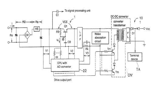
FIG. 1 is a main circuit diagram of a telephone line power utili~tion circuit 101
including a signal separation circuit 1 in accordance with one embodiment of theinvention.
In the above mentioned telephone line power utilization circuit 101, direct-current
power, which is separated from a line signal imputted from the telephone line side
through a bridge diode BD and a hook switch HS by a DC separation transistor Ql, is
supplied to a line terminal device main-body circuit TA through a low-pass filter LPF, a
DC-DC converter CN and a diode Dl.
Vcc is an external power source such as batteries or the like to constitute a power
source for the line terminal device main-body circuit TA when the output from the DC-
DC converter CN is insufficient.
The alternate-current component (signal component) is applied to a signal
proce-scing circuit (not shown) of the line terminal device main-body circuit TA and is
processed after passing through a direct-current blocking capacitor Cl and the hook
switch HS.
The base current IB of the DC separation transistor Ql is comprised of the direct-
current component taken out from the line signal by a base resistance RB and a base
c~p~citor CB, but it is controlled by changes in bias control current Iu by a CPU 22
having an AD converter.
-
2097448
The CPU 22 having the AD converter detects the collector voltage Vl and the
emitter voltage V2 of the DC separation tr~nsistor Ql, detects a voltage VCE between the
colle,ctor and the emitter based on the difference thereof and ch~nging the bias control
current Iu by controlling a control port CP so that the voltage VCE between the collector
and the emitter becomes a predetermined proper value.
In this way, the voltage VCE between the collector and emitter is maintained at a
predetermined proper value to minimi7e losses.
A plurality of taps are provided on the primary side of a converter transformer of
a DC-DC converter CN, and switching elements Trl-Trn are connected to separate ones
of these taps.
The CPU 22 having the AD converter alternatively selects and operates one of theching e1ement~ Trl-Trn, and switches the number of turns of a primary winding ofthe converter transformer of the DC-DC converter CN, and performs an action such that
the input direct-current resistance Rl of the DC-DC converter CN Attains a maximum
value in a range equal to or less than 300n of a direct current resistance of the line
terminal e~uipment viewed from the telephone line-side.
As a result, the direct-current power supplied from the telephone line can be
effectively received.
FIG. 2 is a flow chart showing operations of the CPU 22 having the AD
converter.
When the hook switch HS is in an OFF hook state (step STl), the voltage V3 in
FIG. 1 is dete,cted (step ST2), and line current I is calculated (step ST3) by
I = V3 / Rk
2097448
where, Rk represents the resistance value of the current detecting resist~nce.
Next, it is de~~ ined whether or not the line current I reaches the minimum
current (approximately 15 mA) (step ST4). If the line current I does not reach the
minimum current, the process proceeds to step ST5, and if it reaches the minimumcurrent, the process proceeds to step SU6.
In step ST5, the DC-DC converter CN is switched off, and the process returns to
step ST2.
In step SU6, the DC-DC converter CN is switched on. At this time, the
alternatively s~lected switching element in operation is stored in the memory as a
switching element. When the switching element is not stored in the memory, a switching
element in which the number of turns of the winding becomes minimum (at this time, the
input direct-current recist~nse Rl of the DC-DC converter CN becomes minimum) is
~CS~
In the next step, voltages Vl and V2 in Fig. 1 are detected (step ST7), and the
voltage VCE between the collector and the emitter of the DC separation transistor Ql is
calcul~t~l (step ST8).
Next, the voltage VCE is coll-pared with a proper value (step ST9). This proper
value is, for example, 1/2 the amplitude (2V in case of modem) of the signal co~,-ponent.
If the voltage VCE is greater than the proper value, then the process proceeds to
step ST10. If the voltage VCE is less than the proper value, then the process proceeds to
step STl 1. If the voltage VCE is equal to the proper value, then the process proceeds to
step ST12.
_5_
-
209~448
In step ST10, the control port CP is controlled to increase the bias shunt resist~nce
value and to decrease the bias control current Iu. Thus, the bias current IB becomes
large and the collector-emitter voltage VCE tends to be smaller.
In step STll, the control port CP is controlled to make the bias shunt resi~t~nce
value small and to increase the bias control current Iu. Thus, the collector-emitter
voltage VCE tends to be larger.
Finally, the collector emitter voltage VCE is made to converge to the proper value
though the operations from step Sl'7 to step STl1. For this reason, it becomes possible
to use a transistor having a small rating.
In step ST12, the voltages Vl and V3 are detected.
Next, the direct-current resistance RS of the telephone line power utilization
circuit 1 viewed from the telephone line-side is calculated (step ST13) using equations,
I = V3 / Rk and
RS = (Vl/I) + (RD + RH).
In the next step, the direct-current resistance RS calculated using the above
equations is compared (step ST14) with 300n (preferably, a little less than 30052). If the
re~i~t~nce RS is greater than 300n, then the process proceeds to step ST15. If the
re~ist~nce RS is less than 300n, then the process proceeds to step ST16. When the
rç~ t~nc~ RS e~luals to 300Q, the process returns to the step ST2 desribed earlier.
In the step SU15, a switching element, with smaller number of winding turns thanthe present is selected. Thus, the direct-current resistance RS changes to attain a smaller
-6-
N'
2~9~4~8
value. Thereafter, said switching element is stored in the memory, and then the process
returns to step ST2. In the step SUl6, a switching element, with more winding turns
than the present is se1e~ted. Thus, the direct-current resist~nce RS changes to attain a
larger value. Thereafter, said switching element is stored in the memory, and then the
process returns to step ST2.
In this way the direct-current resi~t~nce RS is made to converge to 300n by the
operations from step STl2 to step SUl6.
As a result above, the loss of DC separation transistor Ql becomes minimum and
the input direct-current resistance Rl of the DC-DC converter CN becomes largest within
the possible range, effectively receiving the direct-current power suppled from the
telephone lines.
The inputted direct-current resistance Rl of the DC-DC converter CN may be
controlled by cll~nginE the duty ratio for pulse driving the switching element(s) Trl (or
Trl-Trn) instead of (or including) the control of switching the taps of the primary-side
winding of the converter transformer of the DC-DC converter CN.
In the signal separation circuit of this invention, the loss in the transistor for
se~a-~ling the direct-current power can be maintained at a minimum value. Therefore, it
is possible to use transistors having a small value of rating.