Note: Descriptions are shown in the official language in which they were submitted.
-2-
~~~'~:~~3
BACKGROUND OF THE INVENTION
1. Field of the Invention
The present invention is an electronic
ballast device for controlling the power to one
or more gas discharge lamps, specifically,
fluorescent lamps. It is directed to the
problems of present ballasts used for fluorescent
lamps which waste energy through excess heat
generation and which also lack control options.
The present invention is able to power any
of the conventional fluorescent lamps without
modification. This includes, but is not limited
to standard fluorescent lamps, H0, VHO, T8, T10,
and T12 lamps ranging from a two foot standard
lamp to an eight foot T12.
-2-
-3-
2. Prior Art Statement
Fluorescent lamps are used extensively
throughout office buildings, schools, hospitals,
industrial plants for lighting, as plant grow
lights for outdoor lighting, and for many other
uses. The power to these lamps are controlled by
ballasts which have inherent problems. While
fluorescent lamps with standard ballasts and less
sophisticated electronic ballasts offer some
benefits over other lighting techniques, such as
lower energy use for comparable light output,
these ballasts still waste energy through
excessive heat generation and they lack the
features available with the present invention.
Standard ballasts use bulky energy wasting
transformers to create a high voltage, low
-3-
-4-
frequency signal to excite the lamp filaments.
The present invention uses a low voltage, high
frequency signal to excite the filaments.
Existing ballasts require specific impedance
matching to a specific lamp design. The present
invention can power a wide range of lamp sizes
without modification.
Using the present invention, lamps will burn
cooler, last longer and produce a brighter light
while using less electricity. The present
invention also has a more sophisticated level of
control then is available from the present state
of the art. It can dim the lamps, delay power-up
to improve lamp life, sense when a lamp is
missing or burnt out and respond accordingly by
reducing power or shutting down completely, and
-4-
it can be controlled remotely or by a
programmable unit.
The present invention does not require that
the lamp be individually matched to the ballast
design. The present design can power a standard
425 ma lamp, an 800 ma HO lamp, a 1500 ma VHO
lamp a T8, a T10 or a T12 lamp without
modification. Prior Art requires the impedance
of each lamp to be matched to the ballast in
order that lamp current be limited. The present
device uses the performance characteristics of
the transformer at the operating frequency
(typically about 38 kHz) that allows the
impedance of the lamps in combination with the
reactance of the transformer windings and a
slight frequenscy change to limit lamp current.
-5-
r
Ei ~ ~ ~ ~ :~
-6-
International Patent No. WO 83/02537 uses a
much lower frequency (20 kHz). While it uses the
frequency characteristics of the output
transformer to dim the lamp by increasing the
frequency, its steady state operation is in the
frequency mid-band of the transformer. This
coupled with the lower frequency (transformer
reactance is proportional to frequency) means
that during steady state operation, the lamp load
must be matched to the ballast. Each additional
lamp requires an additional output transformer. ..
Further, this design requires an additional
transformer in the timing circuit.
U.S. Patent 4,853,598 discloses a higher
frequency device (30 kHz), but one that operates
in the frequency mid-band of the output
-6-
2~9"~~~i~
_, _
transformer. This design dims by lowering
voltage and must also be tailored to match the
load of each lamp.
U.S. Patent 4,998,045 discloses a device
which operates in the frequency mid-band of the
output transformer, and dims by varying the pulse
width (duty cycle) and frequency of the timing
circuit. This ballast must also be matched to
the load.
U.S. Patent 4,998,046 discloses a complex
device with separate transformers for arc voltage ..
and filament voltage. Additional lamps require
extra transformer winding and additional ballast
capacitors to match the new load.
While Prior Art is extensive, none of the
patents disclose an electronic ballast which
_8_
takes full advantage of the characteristics of
the output transformer such that any size lamp
can be powered without impedance matching by
adding or changing components.
SUMMARY OF THE INVENTION
The present invention is directed to an
electronic ballast device for the control of gas
discharge lamps such as fluorescent lamps. The
device is comprised of a housing unit with
electronic circuitry and related components. The
device accepts a.c. power and rectifies it into
various low d.c. voltages to power the electronic
circuitry, and by use of a doubler circuit, to
one or more high d.c. voltages to supply power
for the lamps.
Both the low d.c. voltages and the high d.c.
_g_
2~~~~
-g_
voltages can be supplied directly, eliminating
the need to rectify a.c. power.
The high voltage d.c. power is applied to
a plurality of MOSFET's [Metal Oxide
Semiconductor Field Effect Transistors] which are
controlled by a Pulse Width Modulation [P.W.M.]
circuit which outputs two pulse trains 180
electrical degrees out of phase with each other.
The PWM circuit controls switching circuitry
which switches the MOSFET's such that a high
frequency output is fed into a plurality of
output transformers. Power from the output side
of the transformers is fed to one or more
fluorescent lamps. The PWM circuit thus controls
the frequency which is supplied to the lamps.
The electrical characteristics of the
_g_
~,
-10-
transformers and the impedance of the circuit are
chosen so that two important features are
derived. The transformer operates in its "high
frequency zone" where an increase in frequency,
with voltage held nearly constant, will cause a
decrease in output current. This allows for the
ballast to dim the lamps by increasing the
frequency range. Secondly, in this region of
operation the reactance values of the transformer
primary windings and the transformer secondary
windings become significant. Because reactance
is proportional to frequency, with a steady state
operating frequency of about 38 kHz, these values
are large. When different lamps are installed,
the impedance of the lamp becomes part of the
overall impedance reflected back to the MOSFET's.
-10-
_. . .._ . _ __. .', . _. .._
-11-
As lamp current increases, the resistance of the
lamp decreases allowing for a further current
increase. The overall impedance of the output
transformers coupled with the impedance of the
lamp with a slight frequency change acts to limit
the lamp current. For any of the lamp sizes
installed, a different, steady-state operating
point for current and frequency is achieved when
voltage is held nearly constant. It is the
phenomenon of the transformer characteristics at
the design nominal operating frequency which
allow different lamp loads to be powered without
rewiring or component change.
The high frequency of the voltage applied to
the lamps striking the filaments, causes the
lamps to light. The present invention can dim
-11-
A
1t sJ ~ ~.'"
-12-
the lamps by increasing the frequency inputted to
the transformers thereby causing the output
current to lower while the voltage is held
constant. As the current decreases, the lamps
dim. Thus, it can be seen that the selection of
the operating frequency and corresponding
frequency response of the output transformer are
critical in the design of the present device.
If one or more lamps is burned out or
removed, the device will sense this and either
shut down completely or decrease output power to
the remaining lamps as required.
The present device operates with a higher
efficiency than conventional ballasts and higher
than most electronic ballasts in large part
because of the higher frequency and
-12-
~a~~~~~
corresponding smaller output transformers
required.
The lamps operated by this device will also
last longer. The combination of small constant
voltage on the filaments, lower voltage between
filaments and higher operating frequency cut
down on filament sputtering, and lower the
voltage potential at the levels of the lamp so
that the phosphorus in the lamp is depleted
evenly from end to end. This will increase lamp
life by as much as six times.
According to a still further broad aspect
of the present invention, there is provided an
electronic ballast for controlling the power to
a set of one or more gas discharge lamps. The
electronic ballast comprises a switching circuit
for generating a high-frequency a.c. voltage. A
waveshaping circuit is provided for smoothing
the high frequency a.c. voltage. At least one
transformer is provided and has a primary
winding and at least one secondary winding.
Each of the primary and secondary windings have
a first end and a second end. The switching
circuit, waveshaping circuit and primary winding
are connected together in series. The set of
one or more gas discharge lamps and the at least
one secondary winding is connected in parallel
with the waveshaping circuit such that the first
end of the at least one secondary winding is
connected to a node between the primary winding
and the waveshaping circuit.
BRIEF DESCRIPTION OF THE DRAWINGS
The present invention will be more fully
understood when the present specification is
taken in conjunction with the appended drawings.
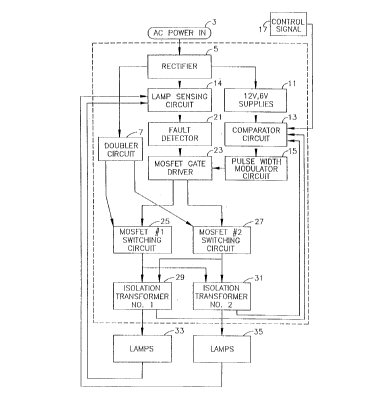
Figure 1 illustrates a flow diagram of the
-13-
electrical process of preferred embodiments of
the present invention; and,
Figure 2 illustrates an electrical
schematic diagram of one preferred embodiment
ballast of the present invention showing the
detailed interrelationships of the various
components.
DETAILED DESCRIPTION OF THE PRESENT INVENTION
The present invention involves an electronic
ballast device for controlling one or more gas
discharge lamps such as a fluorescent lamp. The
flow chart in Figure 1 presents one embodiment of
the present invention shown generally as frame 1.
In this configuration there is an input of
a.c. power 3 by means of a neutral lead and a hot
lead (120 volts in the present embodiment). The
-14-
device has the means to connect to the a.c. power
3. The a.c. power is input to the rectifier
section 5. The rectifier 5 performs several
functions. It rectifies the a.c. power 3 into
various low d.c. voltages 11 as required to power
the electronic circuitry of the device 1.
The rectifier section 5 also converts the
a.c. power 3 into a high voltage d.c. power.
This power is converted by the rectifier 5 and
doubler circuit 7 from the a.c. voltage 3 into
the d.c. power voltage 7. (In the present
embodiment this results in 375 volts d.c.
relative to ground.)
The doubler circuit 7 supplies d.c. power
and ground to two MOSFET's 25 and 27. The
switching of the MOSFET's is controlled by gate
-15-
f
' ~~~~;~~-a
-16-
driver circuitry 23 which in turn is controlled
by the Pulse Width Modulated [PWM] circuit 15 in
the control section described below. The
MOSFET's 25 and 27 are fired alternatively
between the high voltage and ground, at 180
electrical degrees apart such that a high
frequency output is fed into the inputs of the
two isolation transformers 29 and 31, which see a
high frequency symmetrical, alternating signal
relative to the neutral lead which, with
filtering, approaches a sinusoidal wave. ..
The outputs of the isolation transformers 29
and 31 are fed to the means to connect to the
fluorescent lamps 33 and 35. One or more lamps
may be connected to each transformer.
There is also an output of each of the
-16
2~~~1~
-17-
transformers, 29 and 31 which is connected to the
comparator circuit 13 described below.
The comparator circuit receives an
externally generated control signal 17 and
compares this signal to feedback signals from the
outputs of the transformers 29 and 31. The
control signal can turn the device on and off or
can control dimming of the lamps. The comparator
circuit 13 inputs timing signals to the PWM
circuit 15. This PWM circuit 15 sends the timing
signals to the MOSFET gate driver 23 as described ..
above. By controlling the firing of the MOSFET's
25 and 27, the output of the MOSFET's 25 and 27
will be a voltage wave form of variable
frequency. The high frequency voltage excites
the filaments of the fluorescent lamps causing
-17-
r
2~~'~'' ~~
-18-
them to light. By changing the frequency
slightly, proper operating conditions will be
achieved. By increasing the frequency, the lamps
can be dimmed. By preventing the firing of the
MOSFET's 25 and 27, the lamps are shut off
completely.
There is a lamp sensing circuit 19 which can
detect a fault. A power signal from the
rectifier 5 and feedback signals from the lamps
.33 and 35 are input to the lamp sensing circuit
19 which senses the current draw of the lamps. ..
The lamp sensing circuit 19 feeds into the fault
detector circuit 21 which detects when a fault
occurs. A fault occurs when one or more lamps
burn out or when one or more lamps are missing
causing a load change thereby changing the
-18-
-19-
current draw of the load. If such a fault is
detected, the fault detector 21 causes the MOSFET
gate driver 23 to change the signals to the
MOSFET switching circuits 25 and 27 so that power
to the lamps is decreased or completely shut off.
Referring now to Figure 2, a schematic
diagram 101 shows details of a preferred
embodiment of the present invention. Segments
103 and 105 show the 120V a.c. mains input. This
a.c. signal is used in three ways: To supply
high voltage bias to a power switching network, ..
to be used in a 12V power supply, and to be used
as an offset voltage in the transformer network.
Fuse 119 serves as an over current protection
device.
The a.c. voltage is rectified by 1000 ~.rF
-19-
,_.____._,:._ .._......_ ~..
' ~ i~ ~' '~ ' ~'
-20-
power capacitors 129, 155, and diodes 127 and
153. A byproduct of the rectification process is
that the output voltage is doubled to
approximately 325V across wire 131 to wire 157.
When 103 is positive, 153 conducts and charges
155. When 103 is negative, 105 is positive and
charges 129. When 103 returns positive, 129
discharges and make the negative reference of 155
approximately 180V d.c. Capacitor 155 charges
and adds another 180V to the negative reference,
resulting in approximately 360 to 375 volts at ..
the junction of 153 and 155 relative to the
junction of 127 and 129. This voltage serves as
the working voltage for the switching network to
be described later. The junction of diode 127
and capacitor 129 is connected by wire 131 to
-20-
'~.
P
-21-
ground 133 for the system. Resistor 159 (16.2
kS2) serves as a drain device to bleed off the
high voltage stored in the power capacitors 129
and 155.
The rectified voltage is stepped down
through 2.5 kS2 power resistor 115 and used to
derive the 12V power supply voltage. Resistor
115, connects to voltage regulator 109 by wire
107, which regulates its output voltage to
approximately 30V using reference resistors 117
( 8 2 S~ ) and 111 ( 1. 8 kS2 ) . The output voltage of
109 on wire 113 is filtered by 470 ~F capacitor
123 to remove any ripple voltage. The regulator
output, taken at the junction of the output pin
of 109 and capacitor 123 (wire 113) is then used
as bias voltage for the switching FET 141. The
-21-
..___._. _~._._.._.. _ < . .::
-22-
gate of FET 141 is connected to wire 149 which
connects to 150 kS~ resistor 147 from the a.c.
line 125. This drain voltage is regulated at 24V
by the zener diode 135, the zener diode 137, and
30.1 kS2 resistor 139 which steps the 24V down to
6V on wire 143 for use in the comparator network
to be described later. The source voltage is
regulated at 12V on wire 145 for use as the
voltage supply for the electronic components.
TRANSFORMERS
One side of an 85 turn primary winding 213
is oscillated in parallel with an 85 turn winding
183 of a second transformer by the switching
signal at the junction of the source of MOSFET
177 and the drain of MOSFET 165. The other side
of 213 is connected to the one turn secondary
-22-
v sJ i
-23-
winding 253, the waveshaping network of .033 ~rF
capacitor 205 and varistor 209 by wire 207, and
also to filament 602 of lamp 600 by wire 401.
The switching signal generated by the MOSFET
network is essentially a square wave, and this
signal must be conditioned before it is connected
to the lamps. Capacitor 205 smooths the signal
and varistor 209 protects against any overvoltage
spikes, resulting in a symmetrical wave
approximating a sinusoidal waveform. The
secondary winding 253 on one side is connected to
the primary, while the other side is connected by
wire 403 to the other side of filament 602 of
lamp 600. This creates a small differential
voltage across filament 602. On the other side
of 600, one side of the filament 604 is tied to
-23-
one side of a two turn secondary winding 259.
The other side of filament 604 is connected to
one side of filament 702 of lamp 700. The other
side of winding 259 is connected by wire 407 to
the opposite side of filament 7U2. Secondary
winding 255 (one turn) has each side connected to
opposite sides of filament 704 of lamp 700 by
wires 411 and 413 respectively. Thus all
filaments have a small voltage across them. The
side of 255 connected to 411 is also connected to
the a.c. bus 125 connected by wire 199 through
the center of toroid 201. This gives winding 255
an offset voltage with which to excite the lamps,
so that there is a voltage between the filaments
of each lamp, which is about equal to the voltage
across primary winding 213.
-24-
r;
~,. , ~ w
' ' 3
. wii~~~-~?
-25-
Secondary winding 257 (one turn) acts as a
current sensing device and is used as an input to
one of the auxiliary lamp sensing circuits to be
described later. One side of 257 passes through
diode 247, while the other is connected to the
ground 299 by wire 277.
The function of the second transformer
mirrors the first, as they are operated in
parallel. The primary winding 183 is excited by
the same MOSFET switching signal as the first
transformer from wire 181. Capacitor 195 (.033
~rF and Varistor 193 shape the square wave into a
sinusoidal wave to wire 189 connected to winding
183.
The secondary winding 331 (one turn) on one
side is connected to the primary by wire 185,
-25-
while the other side is connected to the filament
802 of lamp 800 by wire 415. The primary is
connected to the other side of the filament 802,
which creates a small differential voltage
difference across filament 802. On the other
side of 800, one side of filament 804 i.s tied to
one side of secondary winding 337 (two turn) by
wire 417. The other side of filament 804 is connected to
filament 902 of lamp 900 by wire 421. The other
side of filament 902 is connected to the
remaining side of secondary winding 337 by wire
419. Secondary winding 333 has (one turn) one
side connected to filament 904 of lamp 900 by
wire 425 and the other connected to the other
side of filament 904 by wire 423. The side of
333 connected to 425 is also connected to the
-26-
w
rectified a.c. bus 125 connected through a jumper
wire through the center of toroid 309. This
gives winding 335 an offset voltage with which to
excite the lamps so that there is a voltage
between the filaments of each lamp, which is
about equal to the voltage across primary winding
183.
Secondary 335 (one turn) acts as a current
sensing device and is used as an input to one of
the auxiliary lamp sensing circuits to be
described later. One side of 335 passes through ,.
diode 271, while the other is connected to the
ground 299 by wire 277.
FAULT DETECTOR
In the absence of a lamp load, or the
presence of an excessive load, the MOSFET
-27-
-28-
switching network operates in a severe
overcurrent mode. This condition will persist in
the initial steady state, as there are only
filaments acting as a load, since the lamps are
not yet ionized. Therefore, a fault detector
circuit is required. The operation of the
circuit is as follows.
A reference voltage is established at the
high input of comparator 805 by the resistive
network of 20 kS2 resistor 817 and 10 kS~ resistor
809. These resistors form the reference with a
simple voltage divider using 12V supply 815,
which has been filtered by 1 uF capacitor 813
connected between 12V 815 and ground 839. The
sensing input from wire 381 passes through series
10 kS2 resistor 801 and terminates at the low
-28-
input of 805. When this input is below the
reference level at the high input (ie, as during
a fault condition), the output of 805 is high.
When the input is above the reference value
(normal operating conditions), the output of 805
is low. Resistor 823 (3.3 M~) is used to
stabilize the output of 805 against oscillation
and is connected between the output pin and high
input of 805. Resistor 831 (10 k~) serves as a
pull up resistor between the output pin of 805
and the 12V supply line. Any noise at this
output is removed by the 1 uF capacitor to ground
843. Under normal operating conditions, the
output of 805 will first be high, and then drop
to low. This is because as the lamps are first
started, they appear similar to a fault
-29-
condition, and then after they are lit settle
down and appear as a normal load. If the lamps
fail to strike, as in a fault condition, the
output of 805 will remain high.
The output of 805 is fed into the trigger
input 859 of a timer chip 855. This timer chip
is configured to act as a time delay one-shot
circuit. The length of the delay is determined
by the combination of 2.2 MS2 resistor 835 and 1
uF capacitor 847. The junction of 835 and 847 is
connected to both timing pins of 855 by wires 857
and 851. The supply 863 and reset 861 pins of
855 are shorted together and tied directly to
the 12V 815 supply line. The ground pin of 855
is tied to the ground bus by wire 849.
When the output of 805 falls low, the
-30-
falling edge triggers the timer of 855 to start
operating. After the delay, determined by 835
and 847, the output of 855 goes high and remains
high. If the output of 805 remains high, there
is no falling edge, and the output of 855 remains
low.
The output is buffered from the next
comparator stage by the series 1 MS2 resistor 889,
and any noise is removed by 1 uF capacitor 869.
A reference voltage is established by equivalent
2.2 MS2 resistors 873 and 891 connected between
12V d.c. and ground, and their junction connected
to the high input of 883. The low input to 883
is taken from the junction of 889 and 869. When
the input 855 is low, the output of gg3 remains
high, only going low when the input rises above
-31-
_.
~~~~~~~~'~
-32-
the level determined by 873 and 891. This output
is stabilized by 3.3 MSS resistor 879 connected
between the output pin and the junction of 873
and 891 which connects to the high input of 883.
The last component of this section is the 499 kS2
pull up resistor 875 connected between the output
of 883 and the 12V supply line.
The output of 883 is then connected to the
shutdown pin of the MOSFET driver 341 by wire
345. When this signal is high, no oscillation
occurs. When the shutdown signal is low,
oscillation is allowed as normal.
MOSFET GATE DRIVER
The MOSFET gate driver circuit is used to
ensure proper turn on at the gates of MOSFETs 177
and 165, ie, no reverse currents and proper gate
-32-
voltage.
The 12V supply line provides power to the
gate driver 341 by wire 349. The grounding for
341 is at wire 351 which is also connected to
wire 339. Wire 351 connects to wire 163 which
ties to ground 133. Wires 347 and 343 are the
inputs to 341 for the oscillating square wave
from the pulse width modulation. In effect, 347
and 343 are two of the three control signals. As
long as wire 345 (the shutdown input) remains
low, these inputs will allow gate driver 341 to
control the switching outputs. When a voltage is
applied to wire 345 from the fault detector
circuit, the outputs of gate driver 341 are
disabled until the voltage at wire 345 falls to
zero.
-33-
".,,'
~~~~
-34-
The switching outputs of gate driver 341 are
found at wires 169 and 170 with wire 169 being
the low side voltage switch and wire 170 being
the high side voltage switch. The high side
voltage is established by taking the high voltage
at the source of 177 and feeding it through a
bootstrap circuit consisting of 20 52 resistor
363, diode 365, and .1 pF capacitor 361. The 12V
at wire 353 causes diode 365 to conduct after
passing through 363. This section acts as the
charging scheme for capacitor 361. Capacitor 36I
is connected between wire 355 and wire 357.
Capacitor 361 stores the voltage at the source of
177 and uses it as the high side switching
voltage. The junction between capacitor 361 and
diode 365 is connected to gate driver 341 by wire
-34-
r1 ~ ; . G1
2~~'~~~.~
-35-
357.
MOSFET SWITCHING CIRCUIT
MOSFETs 177 and 165 are connected in a half
bridge configuration and provide the high voltage
switching to operate the transformers and drive
the lamps. The high voltage supply at the drain
of 177 is taken from the output of the doubler
circuit at the junction of 153 and 155 by wire
157. Any ripple present at this point is removed
by the .68 uF filter capacitor 161, which is
connected between the high voltage supply and
ground. The gate of 177 is turned on by the high
voltage output of the gate driver circuit, with
S2 resistor 171, connected by wire 173, acting
15 as a buffer to reduce the gate voltage level
slightly.
-35-
When the gate is turned on, the high voltage
supply is switched through to the source of 177,
which is connected to the drain of 165, the
bootstrap circuit connected by wire 183, and the
primary of transformer 213. This is the high
power oscillating signal used to drive the lamps.
The switching signals from 341 on wires 169 and
170 alternate 180 electrical degrees out of phase
so that when 177 is on, 165 is off, so at the
junction of the source of 177 and the drain of
165, the voltage is 325V. When the gate of 177
is off, 165 turns on, making the potential at the
junction equal to ground. The gate of 165 is
turned on in the same fashion as 177, with 20 ~
resistor 167, connected by wire 175, acting to
soften the gate turn on voltage.
-36-
PULSE WIDTH MODULATOR CIRCUIT
The pulse width modulator (PWM) circuit uses
a PWM chip 671 to supply the timing signals to
the MOSFET gate driver circuit, and ultimately
control the frequency of MOSFET oscillation.
These timing signals may be generated by other
means but in this embodiment this PWM circuit
supplies the alternating, high frequency timing
signals.
Power for PWM 671 comes from the 12V supply
line connected by wire 661. Capacitor 693 (10
uF) acts as a local filter from the 12V line to
ground by wire 691. The 12V supply is also
connected by wires 669 and 663 to the collectors
of the chip's output transistors, and this
voltage simply serves as the bias voltage for
-37-
-38-
them. Grounding 651 for PWM 671 is supplied by
695, which is also connected to the dead time
control pin by 679, non-inverting input #1 by
673, and non-inverting input #2 by 647. The
regulated reference output is connected by 655 to
657, 653, and 645. A .1 uF capacitor 641 is
connected from 653 by 639 to ground 651 by wire
643 to smooth the d.c. voltage. This d.c.
voltage serves as the inverting input for the
error amplifiers of PWM 671, as well as the
output control voltage. The timing for 671 is
determined by the combination of 22.6 kS2 resistor
697 and 1000 pF capacitor 701 connected to ground
by wire 699. Resistor 697 is connected to PWM
671 by 683 and 649 to ground, while capacitor 701
is connected from wire 681 to ground. At the
-38-
-39-
junction of 697 and wire 683 is attached one side
of 16.2 kS2 series resistor 635, which affects the
frequency of oscillation based on the dimming
signal to be described later.
The outputs of PWM 671 are taken from the
emitters of the output transistors, at wires 665
and 667. These outputs are then connected to
inputs of gate driver 341. Resistors 377 and 379
(10 kS2 each) are shunted across each output line
respectively by wires 373 and 375, to ground 371
to stabilize the outputs locally.
DAMP SENSING CIRCUIT
The output of the toroid at 203 and 217,
represent the current passing through the
secondary winding 255. This is an a.c. voltage
and must be rectified to d.c. Diodes 219, 221,
-39-
-4U-
,
223 and 225 are configured in a full wave bridge
rectifier formation. The full wave rectified
signal is then filtered through .1 uF capacitor
227 to remove the ripple voltage. Capacitor 227
is connected on one side to the junction of 219
and 221, and on the other side to the junction of
223 and 225. The input to the shutdown circuit
is also taken from this point, and is connected
to resistor 801 by wire 381. Resistors 229 and
231 (182 S2 each) serve as a bleeder for capacitor
227 connected by wire 235. These resistors are
equivalent and can be replace by one resistor
equal to the sum of two. It is not critical to
this embodiment that the two resistors be in
series. Diode 275 and .1 ~rF capacitor 279 couple
the junction of 227 and 229 to ground.
-40-
The operation of the second lamp sensing
circuit mirrors the first, much as the
transformer operation is the same. The outputs
of the toroids, across 311, represent the current
passing through the secondary winding 333. This
is an a.c. voltage and must be rectified to d.c.
Diodes 315, 319, 321 and 317 are configured in a
full wave bridge rectifier formation. The full
wave rectified signal is then filtered through .1
uF capacitor 332 to remove the ripple voltage.
Capacitor 332 is connected on one side to the ,_
junction of 315 and 319, and on the other side to
the junction of 317 and 321. This junction is
connected to the junction of diodes 223 and 225
by wire 325. The input to the shutdown circuit
is taken from the junction of 315 and 317 and is
-41-
connected to resistor 801 by wire 381. Resistors
327 and 329 (182 S2 each) serve as a bleeder for
capacitor 322. These resistors are equivalent
and can be replaced by one resistor equal to the
sum of two. It is not critical to this
embodiment that the two resistors be in series.
The circuitry that remains in the lamp
sensing circuit is not critical to the operation
of the ballast. However, the extra circuitry
provides alternate means to implement current
sensing, fault detection, and dimming modules.
The present embodiment leaves these circuits
intact for development of future embodiments.
Diodes 243, 245,261, and 263 are used to
sum together the outputs of the dual toroidal
full wave bridge circuits. Essentially, they act
-42-
~,. .,
as another full wave bridge stage. The junction
of 263 and 243 is connected by wire 249 to the
junction of resistors 571 and 575 in the
comparator network, to be described later. The
junction of 245 and 261 is connected by wire 251
to the junction of resistor 505 and capacitor 511
in the comparator network.
Diode 247 passes only the positive portion
of the lamp sensing signal from winding 257.
This positive portion is then summed with the
positive portion of winding 335, which has also
passed through diode 271. The junction of 271
and 247, wire 269, which is always a positive
voltage, is applied to the gate of FET 301, first
passing through 16.2 kS2 resistor 289, resistor
289 being connected to the diode junction by wire
-43-
a ~ ~~
-44-
287 and to the gate by wire 303. The voltage at
the gate is divided by the resistive network of
289, 3.8 kS2 285 and 5 k potentiometer 281. This
network is used to set the turn on voltage for
the gate of the FET 301 by adjusting the value of
281. Capacitor 295 (22 uF) filters out any noise
between wire 303 and ground on wire 297, which
may have infiltrated the signal coming from the
windings 257 and 335. Capacitor 305 (.1 uF)
serves simply to couple the drain voltage of FET
301 by wire 307, to the voltage coming from pin 1
of comparator 629 through wire 501. The source
of FET 301 is connected to ground 299 by wire
297.
COMPARATOR CIRCUIT
The 6V supply 531 derived in the power
-44-
a
-45-
supply section here acts as a reference voltage
at the high input of comparator 525. The 6V
supply 531 is filtered by .1 uF capacitor 541
from 531 to ground 513 and stabilized locally by
9.91 kS2 resistor 537 shunted from 531 to the
ground 513. The low input gets its level from
the regulated 5V output from wire 637 in the PWM
circuit. Since this comparator is in the
inverting mode, the output to wire 523 will be
high. The output rises slowly, as it charges 22
uF capacitor 517 connected between the output and ..
ground 513. The speed at which the output rises
is controlled by the pull up resistor 521 (45 k).
The smaller the value of 521, the faster 517 will
charge. Resistor 521 is connected on one side to
the output of 525 and on the other side to the
-45-
junction of the 12V supply line, and to 10.7 kit
resistor 505. Resistor 505 here works as a pull
up resistor for the junction of diodes 245 and
261, whose potential is nearly ground. Capacitor
511 (.1 uF) is connected between wire 251 and
ground 513.
The output of 525 is also connected to the
high input of comparator 589. The low input of
589 is taken from the regulated 5V output of 671.
The high input of 589 ramps up until it is at a
higher potential than the low input. At this
point, the output rises slowly, since it is
charging 1 uF capacitor 583, whose positive side
is connected to the output of 589 and high input
of comparator 629. The negative side of
capacitor 583 is connected to the ground. The
-46-
'47-
output of 589 is also attached to 100 kS~ resistor
597, which connects to 10 kS2 resistor 547, 1 pF
capacitor 567, and the opto isolator chip 555.
These resistors are used in the dimming mode
which will be discussed later.
Comparator 629 gets a high input from the
output of 589. The low input comes from the
junction of diodes 243 and Z63, which comes into
the junction of the resistors 575 (32.7 kS~) and
571 (100 kS2). Resistor 571 goes between the
junction of diodes 243 and 263 and the ground for
stability, while resistor 575 goes from this
junction to the low input of 629. Also meeting
at the low input of 629 is one side of .047 uF
capacitor 579, connected by wire 577, which is
connected as a feedback capacitor from the output
-47-
a ~!~ "J
'~ s t ! r k
~~ ~ ~ .~~J
-48-
of 629. This input is taken from the lamp
sensing circuit. When the lamps are not yet lit,
the signal is low, but once the lamps light, the
voltage here goes high. The low input goes high
faster than the high input, which is more of a
slow ramp. When the voltage at the high input
finally exceeds the voltage at the low input, the
output of 629 goes high.
The output of 629 is connected to the output
of 619, the low input of 619 by wire 621, the
feedback capacitor 579, and the series resistor
635.
The high input of 619 comes from the low
input of 589 through the 100 kS2 buffer resistor
607. To take out noise at this pin, .1 uF
capacitor 615 is shunted from the high input to
-48-
~~~"t~'_~
-49-
ground. The low input of 619 is connected to the
output of 629. Comparator 619 is used to reduce
the voltage present over resistor 635 at startup.
When the input at the low input finally goes high
as a result of comparator 629, the output of 619
then goes high also.
CONTROL SIGNAL
The control signal is supplied by an
external device which outputs information to
input pins of the optical isolator 555 between
wires 557 and 559. This information can be used
to dim the ballast, or remotely turn the device
on or off. When no control signal is present,
the voltage at the collector of 555 is 5V at wire
553, since it is connected to the regulated
output voltage of 671 though resistor 547. The
-49-
-50-
emitter of 555 is connected to the ground 565 by
wire 561. Capacitor 567, connected from the
collector of 555 to the ground 563, serves as a
noise filter. The control signal, in this case a
dimmer signal, causes a PWM signal to appear at
the collector of 555, and the pulse width of this
signal varies with dimmer input. As the duty
cycle decreases, and the dead time increases at
the collector of 555, the lower average voltage
at this point causes the voltage at the output of
comparator 589 to lower, allowing 583 to drain ..
off. As 583 drains off, the voltage at the high
input of 629 decreases, which causes the voltage
at the output of 629 to drop off. Resistor 635
is the timing interface device between the
comparator section and the PWM section. When
-50-
~~~,~t4,~G,
-51-
voltage is applied over 635, it changes the
effective resistance seen at the resistive timing
of 671. As this effective resistance changes,
the frequency of oscillation increases and the
lamps dim.
For a remote on-off controller, the input to
555 is a d.c. voltage, and this causes the
collector of 555 to fall to zero volts. At this
point, the same characteristics are displayed as
when dimming, except instead of dimming, the
ballast shuts off.
The present invention can be used to power
fluorescent lamps in a wide variety of
applications. It can power fluorescent lamps to
provide light to aquariums, controlled by a
timer. It can power lamps used to provide light
-51-
,.~~ ~, ~.
~~'-~~se
-52
for houseplants, controlled by a photocell
monitoring system.
The present invention can achieve great
energy savings in office buildings, schools,
hospitals and industrial plants or any other
location where there are large banks of lights.
Not only does this type of application where
there are so many lamps benefit from great energy
savings, but it benefits from the ability to
remotely and precisely control the output of the
lamps. Also, since not all lamps in such a
location will necessarily be of the same type,
the user will benefit from the ability to
interchange bulb types without rewiring or
modification.
The present invention is also ideal for
-52
~'d E1
-53-
outdoor applications, lighting either areas or
billboards. Because of the need to provide light
for long periods in remote locations, the
applications will benefit both from the energy
savings of the present invention and from its
ability to control the output of lamps.
Obviously, numerous modifications and
variations of the present invention are possible
in light of the above teachings. It is therefore
understood that within the scope of the appended
claims, the invention may be practiced otherwise
than as specifically described herein.
-53-