Note: Descriptions are shown in the official language in which they were submitted.
W093/09586 PCT/SE92/0071
Reduction of disturbances in a ~ower network
TECHNICAL FIELD
The present invention relates to a method and a device in an
electric power network comprising an active filter, con-
trollable via a control input, for reducing disturbances
generated by a disturbance source located in the power
network and/or connected thereto. The power network may, for
example, consist of a network for transmission of high-
voltage direct current connected to an a.c. network by means
of a static converter.
BACKGROUND ART
Non-linear elements give rise to disturbances in the form of
harmonics in the power networks to which they are connected.
Thus, for example, by its operating principle comprising the
cyclic connections of different parts of the alternating
voltage via the valves included in the convertor, a conver-
tor connected to an a.c. network generates harmonic currents
on its a.c.side and harmonic voltages on its d.c. side.
During the time intervals between the commutations, however,
the convertor may be regarded as a linear element and the
currents and voltages arising in the power network may
therefore, during the above-mentioned time intervals, be
determined from a linear model based on the knowledge of the
phase position and the amplitude of the applied voltage as
well as on the impedance and initial state of the network.
Further, the cyclic connections impart to the currents and
voltages arising waveforms which, during a steady state, are
repeated for the respective time interval. In principle,
only harmonics of the order n=kp +l occur on the a.c. side
and of the order n=kp on the d.c. side, where p is the pulse
number of the converter and k is a positive integer.
To reduce the stresses, originating from the harmonics, on
the components included in the power network and to fulfil
W093/09586 2 0 9 7 6 o o PCT/SE92/00715
the requiremenrs~~ade on the effect of the harmonics on the
network, therefore, filters are generally required to limit
the propagation of the disturbances in the power network.
Especially in plants for transformation between alternating
current and high-voltage direct current, where there are
also placed demands for limitation of telecommunications
disturbances emanating from the lines, extensive installa-
tions for filtering the generated harmonics are required.
These filters are generally built up from passive components
and are tuned to the harmonics of a lower order whereas the
harmonics of a higher order are filtered through a high-pass
filter. When calculating the passive filters, factors such
as resonances with the impedance of the network - which
impedance is dependent on the network configuration - are
also taken into account. The fact that the passive filters,
installed on the a.c. side, are also to serve as members for
generating reactive power is also taken into account.
Drift at mains frequency and in component values means that
an exact tuning generally cannot be maintained, and also at
the resonance frequency the filter impedance will not always
be negligible as compared to the network impedance. In
practice, therefore, harmonics remain in the network and to
this is to be added the fact that during the actual
commutations and due to any phase unsymmetries, harmonics of
other numbers of order than those mentioned above are also
normally generated.
The above-mentioned limitations of the passive filters have
therefore led to proposals for the use of active filters
instead, whereby the network via these filters are supplied
with currents or voltages counteracting those which are
generated by the disturbance source. By measuring the
rem~; n ing harmonic contents in the power network, the
supplied currents or voltages can then, in principle, be
given such waveforms that they completely eliminate the
harmonic contents of the network. Thus, in the IEEE
publication 89 WM 123-l PWRD (IEEE/PES 1989 Winter Meeting,
W093/Og586 PCT/SE92/00715
3 2 ~ 9 76 00
New York 1989): Cheuksum Wong, Ned Mohan, Selwyn E. Wright
and Karl N. Mortensen: Feasibility Study of AC- and DC-Side
Active Filters for HVDC Converter Terminals, there is given
a technical and economic evaluation of a device comprising a
controllable current generator which is intended to be
connected between line and ground in an HVDC station. The
evaluation is based on calculations and on simulations of
the device connected to the direct voltage side. The results
indicate a good technical effect, but as far as is clear
from the report the simulations have been performed only for
steady states while considering harmonics of the orders 12,
24 and 36. Further, a greatly simplified model of the
converter has been used and the effect of the direct voltage
line has been neglected. By this approach it has been
possible to calculate, based on the model, the reference
value of the current which, via the current generator, is to
be supplied to the network to eliminate the harmonics
considered, and this reference value has then been used
during the simulations. The report indicates a method of
controlling the current generator of the active filter by
harmonic analysis of the direct voltage at the converter
and, by feedback via PI regulators, forming a reference
value for the current generator such that the contents of
harmonics of the above-mentioned three orders in the direct
voltage are controlled towards zero.
As mentioned above, the connected power network shows an
impedance with several resonance frequencies, and in fact,
in view of the complicated characteristics in the frequency
domain of an extended power network, control systems based
only on feedback are likely to involve difficult dimen-
sioning problems.
..
Essentially, the control problem is caused by the non-
minimum phase behaviour of the transfer functions of the
electric power network. The physical reason for this
behaviour are electromagnetic waves travelling along the
power lines and their reflections at points with changes in
W093/~ 2 0 9 7 6 0 0 PCT/SE92/00715
the impedance characteristics. This implies multiple trans-
portation delay effects (echoes) on control responses of the
electric power network as the natural damping effect on
travelling waves is very low.
It is well known from text books in control theory, for
example Bernard Friedland, Control System Design, McGraw-
Hill International Editions, 1987, ISBN 0-07-100420-3, pp.
78, 144, 188, note 4.7, and Richard C. Dorf, Modern
Control Systems, Addison-Wesley Publishing Company, Fourth
Edition, 1986, ISBN 0-201-05326-8, pp. 262-264, that non-
minimum phase implies zeroes in the righthand part of the
complex s-plane and it is also impossible to make stable
feedback control with very quick response for non-miniml~m
15 phase systems.
The need to reduce disturbances with a certain frequency
content also exists in other physical processes, and methods
for this have also been published on several occasions.
20 Thus, PCT application PCT/GB80/00128 (WO 81/00638) discloses
a method for reduction of acoustic disturbances, or more
generally vibrations in gases, liquids, or solids, in which
the periodic character of a disturbance source is utilized
in such a way that a signal stored in a memory member is
25 applied, repetitively and synchronized from the disturbance
source, to a loudspeaker placed at a location where the
disturbance is to be reduced. The acoustic pressure genera-
ted by the loudspeaker is given such an amplitude and such a
phase position that it tends to extinguish the original
30 disturbance. The desired cancellation of the disturbance is
thereby obtained in such a way that the resultant acoustic
pressure is sensed by a microphone whereupon, after certain
signal processing, the signal stored in the memory member is
corrected in such a way that it tends to further reduce the
35 resultant acoustic pressure. Specifically, the last-
mentioned publication describes methods whereby the correc-
tion is calculated from a measured value synchronized with
the disturbance source and is added to the contents of the
W093/09586 PCT/SE92/00715
2097600
memory member in a phase-correct manner in view of the
acoustic delay of the system, whereby the magnitude of the
correction can either be given predetermined values or be in
proportion to the amplitude of the resultant acoustic
pressure.
Also EP application No. 88112057.0 (Publ. No. 0 301 483)
describes a controller for a power convertor for systems for
non-interrupted power supply, active filters, etc. The con-
troller comprises a memory member adapted to store a signalcorresponding to the output signal of the controller during
a period of a repetitive sequence. The signal stored in the
memory member is corrected by adding the control error, with
one cycle's time delay, to the contents of the memory.
The introduction of a memory member for storage of signal
values in the controller makes it possible to achieve a good
cancellation of a stationary periodic disturbance, also with
an amplification in the feedback loop which is low for
reasons of stability. However, a low amplification means
that the contents of the memory member is corrected relati-
vely slowly during non-steady states.
The major disadvantage in this case is that delay effects
and other non-m;nimllm phase effects as well as other types
of system dynamics are not included and compensated. In
general, the correction of the memory with the control error
delayed one period will make the controller unstable as
there are implicit or explicit delay effects of the systems
and other dynamics as well. The total delays add up to more
than one period and therefore, even if the controlled system
is stable, the damping effect of disturbances with one
period repetitive patterns is not very high.
6 2097600
SUMMARY OF THE INVENTION
The object of the invention is to provide a method for
reducing, in a power network, disturbances such a harmonic
currents or harmonic voltages, generated by a disturbance
source included in or connected to the power network, and a
device for carrying out the method. The power network may,
for example, consist of a network for transmission of high-
voltage direct current connected to an a.c. network by means
of a converter. The method is to permit a total elimination
of harmonics over a broad frequency spectrum by a dynamically
stable active filtering as well as fast adaptation to non-
steady disturbances.
According to the present invention, there is provided a method
in an electric power network, comprising at least one input
line, at least one output line, an active filter controllable
via a control input as well as a plurality of interconnected
components, for reducing on the output line disturbances
generated by a disturbance source located in, or connected to,
the power network, wherein of the components a first component
group, a second component group and a third component group
are formed such that the input line and the disturbance source
are connected to the first component group, at least the
second component group comprises at least approximately linear
components and comprises the first active filter and that the
output line is connected to the third component group,
a first second (A--A) and a second section (B--B) through the
power network are defined such that the input line and the
disturbance source are located on one side of the first
section (A--A) and the output line and the control input are
located on the other side of the first section (A--A) and that
the control input and the output line are located on different
sides of the second section (B--B) and the second component
group is located between the first section (A--A) and the
-t
6a 2 09 7600
second section (B--B), and that the second section (B--B) does
not intersect the first section (A--A),
at least a first state variable (Yli) is sensed in the power
network,
based on the first state variable (Yli) and a model of the
power network an equivalent impedance for the disturbance
source, as viewed from the first section (A--A), and an
equivalent disturbance voltage generator or an equivalent
disturbance current generator are determined, such that the
voltage generator or the current generator respectively, at
the first section (A--A), would generate at least
substantially the same disturbances (X1) as the disturbance
source,
based on the equivalent disturbance voltage generator or
equivalent disturbance current generator respectively, on the
equivalent impedance and a model of the second component group
and the third component group, those disturbances (X2) are
calculated which occur in the second section (B--B) without
any action from the active filter,
a control signal (C1) is calculated such that, supplied to the
control input, it would generate in the second section (B--B)
the disturbances (X2) calculated by means of the equivalent
disturbance voltage generator or equivalent disturbance
current generator respectively, with reversed polarity, and
that the control signal (C1) is generated and supplied to the
control input.
According to the present invention, there is also provided
a device in an electric power network, comprising at least one
input line, at least one output line, an active filter
controllable via a control input as well as a plurality of
interconnected components, for reducing on the output line
,
6b 2097600
disturbances generated by a disturbance source located in, or
connected to, the power network, wherein of the components a
first component group, a second component group and a third
component group are formed such that the input line and the
disturbance source are connected to the first component group,
at least the second component group comprises at least
approximately linear components and comprises the first active
filter, and that the output line is connected to the third
component group, that a first section (A--A) and a second
section (B--B) through the power network are defined such that
the input line and the disturbance source are located on one
side of the first section (A--A) and the output line and the
control input are located on the other side of the first
section (A--A) and that the control input and the output line
are located on different sides of the second section (B--B)
and the second component group is located between the first
section (A--A) and the second section (B--B), and that the
second section (B--B) does not intersect the first section
(A--A), which device comprises a control member which is
supplied with at least on first state variable (Yli) sensed
on the power network and generates and supplies the control
input with a control signal (C1), which control member
comprises,
a first calculating member which, based on the first state
variable (Yli) and a model of the power network determines an
equivalent impedance for the disturbance source as viewed from
the first section (A--A), and an equivalent disturbance
voltage generator or an equivalent disturbance current
generator, such that the voltage generator or current
generator respectively at the first section (A--A), would
generate at least substantially the same disturbances (X1) as
the disturbance source,
a second calculating member which, based on the equivalent
disturbance voltage generator or equivalent disturbance
6c 2097600
current generator respectively, on the equivalent impedance
and a model of the second component group and the third
component group, calculates those disturbances (X2) which
occur in the second section (B--B) without any action from the
active filter, and
a fourth calculating member which calculates the control
signal (Cl) such that, supplied to the control input, it would
generate in the second section (B--B) the disturbance (~2),
lo calculated by means of the equivalent disturbance voltage
generator or equivalent disturbance current generator
respectively, with reversed polarity.
BRIEF DESCRIPTION OF THE DRAWINGS
The invention will be explained in greater detail, by means
of embodiments, with reference to the accompanying drawings,
wherein:
0 Figure 1 schematically shows a power network comprising a
disturbance source and an active filter,
Figure 2A shows in the form of a block diagram an embodiment
of a control member according to the invention for
the active filter according to Figure 1,
Figure 2B schematically shows equivalent disturbance current
and voltage generators as well as an equivalent
internal impedance for the network according to
Figure 1, seen from the second section B-B,
Figure 2C schematically shows e~uivalent disturbance current
and voltage generat~r~ ~o~ ol~ 9~ t
-
-
W093/09586 PCT/SE92/0071
7 2 0 9~ 6 0 0
internal impedance for the network according to
Figure 1, seen from the third section C-C,
Figure 3 shows in the form of a single-line diagram a pole
of an HVDC station with an active filter and a
control member according to the invention,
Figure 4 shows in the form of a block diagram an embodiment
of a control member according to the invention in
an HVDC station according to Figure 3,
Figure 5 schematically shows how an equivalent disturbance
voltage is formed from voltages supplied to the
control member according to Figure 4,
Figure 6 shows a model for calculating the current
commutation process in the control member
according to Figure 4,
Figure 7 shows a model for calculating the disturbance
current on the d.c. line in the control member
according to Figure 4,
Figure 8 shows in the form of a single-line diagram a pole
of an HVDC station with an active filter and a
control member according to a further embodiment
of the invention,
Figure 9 shows in the form of a block diagram an embodiment
of a control member according to the invention in
an HVDC station according to Figure 8,
Figure 10 shows in the form of a block diagram an embodiment
of a controller according to the invention,
arranged in a control member,
WO 93/09586 2 0 9 ~ 6 0 0 8 PcT/sE92/oo7l5
Figure 11A shows in the form of a block diagram an
embodiment of a compensating filter in a
controller according to Figure 10,
Figure llB shows in the form of a block diagram an
embodiment of a delay-compensating circuit in a
controller according to Figure 10,
Figure llC shows in the form of a block diagram an
embodiment of an attenuation circuit in a
controller according to Figure 10,
Figure llD shows in the form of a block diagram an embodi-
ment of a filter circuit in a controller according
to Figure 10, and
Figure 12 shows in the form of a block diagram an embodiment
of a voltage generator comprised within an active
filter.
DESCRIPTION OF THE PREFERRED EMBODIMENTS
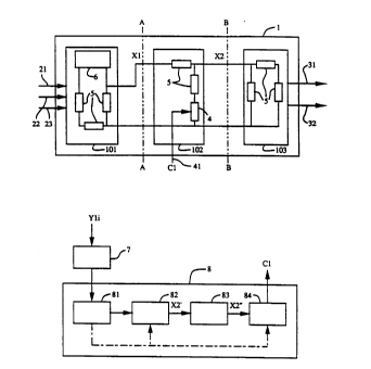
Figure 1 shows an electric power network 1 with three input
lines 21, 22, 23 and two output lines 31, 32. As
schematically shown in the figure, the power network com-
prises a plurality of interconnected components 5 brought
together into three interconnected component groups, a first
101, a second 102 and a third 103 component group. The
second component group 102 comprises components which are at
least approximately linear whereas the first and third com-
ponent groups 101 and 103 may comprise non-linear compo-
nents. In the power network, currents and voltages arise
which contain components which are regarded as disturbances.
The disturbances are generated by a disturbance source 6
present in the power network and/or connected thereto. The
power network comprises an active filter 4 which is arranged
in the second component group 102 and which, in dependence
on a control signal C1 supplied via a control input 41, is
W O 93/09586 PC~r/SE92/00715
9 209~600
adapted to influence at least some current or voltage
occurring in the power network so that the components of the
currents and/or the voltages on the output lines 31, 31,
which are regarded as disturbances, are reduced or eli-
minated. The figure indicates a division of the power net-
work by means of a first section A-A and a second section s-
B. The section A-A iS situated such that the output lines
and the control input are located on one side of the section
and the disturbance source and the input lines are located
on the other side thereof. The second section s-s, which
should not intersect the first section A-A, iS situated such
that it divides the power network between the control input
and the output lines so that the at least approximate linear
second component group 102 is situated between sections A-A
and B-B.
One or several state variables, which are generally designa-
ted Yli and which may consist of currents, voltages, pulse
trains, etc. in the power network, are measured in the power
network (this is not shown in Figure 1 but is performed in a
manner known per se). In the event that it should be or
needs to be defined in the following that the first state
variable Yli is measured at the second section B-B, this
variable, by definition, is given the designation second
state variable Y2i.
The above-mentioned measured values of state variables are
supplied to a control member 8, the function of which is
schematically illustrated in Figure 2A. A measuring device 7
senses, in the manner described above, one or several first
state variables in the power network, these state variables
being indicated in Figure 2A by the general designation Yli.
However, it is to be understood that this designation Yli
may refer to one or more state variables. The measured value
Yli iS supplied to a first calculating member 81, adapted to
calculate, based on the measured state variables and on a
known model of the power network comprised in the first
calculating member, an equivalent disturbance voltage or
W093/09586 ` 2 0 9 7 6 0 lo PCT/SE92/00715
disturbance current generator 62 as well as an equivalent
internal impedance 61 for the disturbance source, seen from
the first section A-A, in a two-pole model, as illustrated
in Figure 2s. The disturbance voltage or disturbance current
generator 62 is determined such that it generates, at least
approximately, in the first section A-A, the same distur-
bance currents and/or disturbance voltages X1 as the
disturbance source. Alternatively, in the event that the
first state variables Yli are measured in the first section
A-A, the first calculating member 81 may be adapted, based
on measured values of at least two state variables Yli in
the first section A-A, for example current and voltage, and
on a model of the power network, to directly calculate an
equivalent disturbance voltage or disturbance current
generator 62 as well as an equivalent internal impedance 61
for the disturbance source, seen from the first section A-A.
Also in the event that only one current or one voltage is
available for measurement in the first section A-A, an
equivalent ideal disturbance current or disturbance voltage
generator may be determined, in which case, however, a
certain feedback effect arises between the influence on the
network by the active filter and the disturbance source. In
many cases, the impedance levels for the component groups
included in the power network are such that, during the
above-mentioned calculations, only the first component group
101 need be taken into consideration.
The equivalent disturbance voltage or disturbance current
generator 62 with the associated equivalent impedance 61,
calculated in the first calculating member 81, is then
applied to a model comprised in a second calculating member
82 and representing the second and third component groups
102 and 103 for calculating the disturbance currents and/or
disturbance voltages X2 occurring in the second section B-B
and generated by the disturbance source, without any action
by the active filter. In this case, the possibly non-linear
third component group 103 may be replaced by an imaginary
linear load or by an open circuit.
W093/09586 ll 2 0 g ~ 6 o ~ PCT/SE92/00715
It is not always desirable to adapt the control member to
reduce or eliminate, via the active filter, all the
frequency components in the disturbance currents or
disturbance voltages occurring in the second section B-B.
The values X2~ of the disturbance currents and/or distur-
bance voltages x2 occurring in the second section B-B,
calculated in this manner, are therefore applied to a third
calculating member 83 adapted to reduce or eliminate in the
calculated values x2~, by filtering, such components X2h as
are not to be reduced or eliminated on the output lines 3l,
32 of the power network. The components X2~ of the calcu-
lated disturbance currents and/or disturbance voltages x2~
then remaining are applied to a fourth calculating member 84
which is adapted, based on the inverted transfer function Gl
between the control signal Cl and the disturbance currents
and/or disturbance voltages X2 in the second section B-B, to
determine an equivalent signal CE which is of such a nature
that, applied to the control input 41, it produces at least
approximately the same disturbance currents and/or distur-
bance voltages X2 in the second section B-B as those cal-
culated in the third calculating member 83, and to generate
a control signal Cl corresponding to the equivalent signal
with reversed polarity, which control signal is supplied to
the control input 41 of the power network. In the event
that, during the calculation of the disturbance currents
and/or disturbance voltages x2, the third component group
103 is replaced by an imaginary linear load or by an open
circuit, also the equivalent signal CE is calculated with
the corresponding model of the third component group.
Thus, in the method described, the components of the
currents and/or voltages X2 occurring in the second section
B-B and regarded as disturbances are reduced or eliminated
by feeding forward a control signal to the active filter,
whereby also the disturbances generated by the disturbance
source and occurring on the output lines of the power
network are reduced or eliminated.
W093/09586 12 2 09 7 6 o o PCT/SE92/00715
It is to be understood that the input and output lines and
control inputs shown in Figure 1 are only shown as examples
and that, in the general case, their number may deviate from
the numbers shown. The parameters included in the second and
fourth calculating members 82, 84 may be given variable
values corresponding, for example, to varying impedance
values for the components 5 comprised in the component
groups. This is illustrated in Figure 2A by a dashed line
from the first calculating member 81 to the second and
fourth calculating members.
The two-pole models shown in Figure 2 consist in the general
case, when more than two state variables are sensed, of
multi-pole models. In the event that the control member is
adapted to reduce or eliminate, via the active filter, all
the frequency components in the disturbance currents or
disturbance voltages occurring in the second section B-B,
the third calculating member 83 may be omitted and the
disturbance currents and/or disturbance voltages X2, calcu-
lated by the second calculating member 83 and occurring inthe second section B-B without any action by the active
filter and generated by the disturbance source, be supplied
to the fourth calculating member 84 .
Figure 3 shows a converter 6 in a 12-pulse connection
included in an HVDC plant, which converter is connected in a
known manner by way of transformers 9 to a three-phase a.c.
network 2 (only indicated in the figure). A harmonic filter
53 is connected to the a.c. network, and this filter also
comprises capacitor banks for generating reactive power. The
neutral terminal 61 of the converter is connected to an
electrode line 52 and its pole terminal 62 is connected to
one of the terminals of a smoothing reactor 54, the other
terminal of which is connected to a pole line 51. A control
unit 10, arranged in a manner known per se, supplies the
converter with pulses FC, which control the ignition of the
valves included in the converter and which also generate
synchronizing pulses S timely related to the pulses FC. The
W093/09 ~ 13 7 6 0 0 PCT/SE92/00715
phase voltages of the alternating voltage network are desig-
nated Uacl, Uac2, Uac3 and the voltage across the converter
is designated Udc. From the pole terminal of the converter
flows the direct current I1 and out on the pole line flows
the pole line current I2. A passive filter 55 is connected
with one of its terminals to the pole line 51 at a first
connection point 111, located, as viewed from the converter,
on the pole line beyond the smoothing reactor, and with its
other terminal it is connected to one of the terminals of an
active filter 4 comprising a controllable voltage generator
42, the other terminal of the filter being connected to a
second connection point 112 on the electrode line. Through
the passive and active filters thus connected in series, the
filter current I3 flows. The passive filter may be designed
tuned and/or as a high-pass filter. The voltages Uac of the
three phases of the alternating voltage network are measured
in a manner known per se by means of a voltage measuring
device 12, which comprises voltage transformers and analog-
to-digital converters, and the direct current I1 is measured
by means of a first current measuring device 13. The power
network 1 described with reference to Figure 1 is represen-
ted in Figure 3 by the a.c. network 2, the harmonic filter
53, the transformers 9, the converter 6, the smoothing
reactor 54, the passive filter 55, the active filter 4, the
pole line 51, the electrode line 52, and a load (not shown
in the figure) connected to the pole line 51. The sections
A-A and B-B described with reference to Figure 1 have been
located in Figure 3 such that the first section A-A inter-
sects the connection between the pole terminals of the con-
verter and the smoothing reactor 54 and the electrode line52 between the converter and the second connection point
112, and the second section B-B such that it intersects the
pole line 51 and the electrode line 52, as viewed from the
converter beyond the passive filter 55 and the active filter
4 but before the load (not shown) connected to the pole
line. The sensed first state variable Yli consists of the
phase voltages Uacl, Uac2, Uac3 of the alternating voltage
W093/09586 PCT/SE92/00715
2097600 14
network, the direct current Il of the converter and the
synchronizing pulses S generated by the control unit 10.
A control member 8, the design of which will be explained in
greater detail with reference to Figure 4, generates, in
dependence on the phase voltages Uacl, Uac2, Uac3 of the
alternating voltage network, the direct current Il and the
synchronizing pulses S, a control signal Cl which is
supplied to the voltage generator 42 via the control input
41.
The first calculating member 81 is supplied with sampled
values of the three phase voltages Uacl, Uac2, Uac3 of the
alternating voltage and with the synchronizing pulses S
synchronized to the firing pulses to the thyristors of the
converter. The first calculating member is adapted, in
dependence on the synchronizing pulses, to select, in a
manner known per se, from a table the phase voltage or
voltages of the alternating voltage which, in dependence on
the commutating state of the converter, is or are connected
to the direct voltage side of the converter, and to form
therefrom a first model voltage Uf in such a way that this
voltage during a commutation sequence is formed as the
difference between the phase voltages for the phases which
are under commutation and between the commutation sequences
as the phase voltage for the phase which is connected to the
direct voltage side of the converter. Further, the first
calculating member is adapted to form a second model voltage
Ue which corresponds to the overvoltage which at the end of
the commutation sequence is generated because of the
recovery charge of the decommutated thyristor. The second
model voltage Ue has a saw-tooth shape and its magnitude is
determined in dependence on the voltage jump when the commu-
tation has terminated and is preferably calibrated on the
installed plant for best accuracy.
In a model arranged in the second calculating member 82 and
representing the impedances included in the commutating
WO93/~K 2 0 9 7 6 0 0 PCT/SE92/00715
circuit, a commutating current Ik is calculated in depen-
dence on the first model voltage Uf for calculating the
commutating sequence. As starting value for the current Ik
in the model, a value of the direct current Il, measured by
the first current measuring device 13 and supplied to the
second calculating member 82, is set, and when the current
Ik calculated in the model has dropped to the value zero,
the commutation has been terminated. Further, the second
calculating member 82 is adapted to comprise a model of the
converter for calculating the direct current Il without any
action by the active filter 4. This latter model is supplied
both to the first model voltage Uf and, when the commutation
according to the previously described calculation is
terminated, to the second model voltage Ue. The time of
terminated commutation is marked in Figure 4 by a signal SlO
from the second to the first calculating member.
Now, if the load, connected to the pole line and not shown
in the figure, is replaced by an open circuit at the second
section B-B, the current Il representing the calculated
value Il' will flow through the series-connected passive and
active filters 55 and 4. If the filters are assumed to have
the total impedance ZF, a voltage US=ZF*Il will then arise
across the second section B-B, and it is realized that in
this case the voltage US contains the same disturbance
frequencies as the current Il. The filtering which is per-
formed in the third calculating member 83 can therefore also
be performed on a calculated voltage US'=ZF*Il'.
The third calculating member 83 is adapted to eliminate,
from the value Il' of the direct current calculated in the
second calculating member, the d.c. component and, to avoid
reduction of these tones via the control member with an
ensuing high load on the active filter, components Ilh of
the fundamental tone of the a.c. network as well as the
second and third tones of the a.c. network. In this case,
the third calculating member comprises a known value of the
total filter impedance ZF and the above-mentioned filtering
W093/09586 2 0 9 7 6 0 0 16 PCT/SE92/00715
is carried out on a calculated voltage US'=ZF*Il~. From the
third calculating member 83 there is thus obtained a calcu-
lated value US~ which corresponds to a calculated current
Il" with the d.c. component and the above-mentioned har-
monics Ilh eliminated or at least reduced. It is realizedthat if the controllable voltage generator 42 comprised in
the active filter 4 is brought to generate a filter voltage
UF with reversed polarity to the voltage US", the distur-
bances corresponding to the calculated value Il" will be
eliminated in the second section B-B, that is, on the pole
line.
The control signal Cl is supplied to the voltage generator
42 which in the circuit, formed by the active filter 4
connected in series with the passive filter 55, between the
pole line 51 and the electrode line 52, thus injects a
filter voltage UF with reversed polarity to the voltage
which those components of the direct current Il, which
correspond to those included in the calculated value Il",
generate in the circuit mentioned. The voltage generator
thereby generates a filter current I3, which at the
connection point 111 between the pole line 51 and the above-
mentioned series-connected circuit is added to the direct
current Il such that, for the processed interference
frequencies, the sum at this connection point becomes zero
or at least near zero. In this way, the above-mentioned
interference frequencies in the pole line current I2 will
also be zero or at least near zero.
Figure 5 shows on the horizontal axis the time t and on the
vertical axis schematically how the first model voltage Uf
is formed from the phase voltages Uacl, Uac2 and Uac3 of the
alternating voltage network. Further, the vertical axis
shows the variation of the second model voltage Ue in time
related to the first model voltage Uf. The horizontal axis
also shows a sequence of synchronizing pulses S, which are
simultaneous with the firing pulses which initiate the
commutating sequences as well as the signal S10 representing
W093/09586 2 0 9 7 6 0 o PCT/SE92/00715
the times for terminated commutation. The disturbance con-
tents of the model voltages will be substantially cyclic
with the cycle time T. In order to render the figure
clearer, the conditions in connection with a 6-pulse
connection are shown. The corresponding voltages in a 12-
pulse connection are formed as the sum of the voltages of
two 6-pulse groups.
Figure 6 shows the model, comprised in the second calcula-
ting member 82, for calculating the commutating current Ik
during a commutating sequence determined by the phase
voltages Uacl and Uac3. These are represented in the model
by two voltage generators 621, 622, the sum voltage Uf of
which at the time shown consists of the difference between
the phase voltages Uacl and Uac3, whereas the impedances
included in the short-circuited commutating circuit are
represented by the reactor 14. The diode 15 with the
capacitor 16 and the resistor 17 represent the thyristors
included in the converter with overvoltage protection in the
form of RC circuits whereas the reactor 18 represents the
smoothing reactor 54.
Figure 7 shows the model, also comprised in the second
calculating member 82, for calculating the current I1~
representing the direct current I1. The first and second
model voltages Uf and Ue, respectively, are represented by
the voltage generators 623, 624. The reactor 19 represents
the inductance of the connected phases, the capacitor 20 and
the resistor 21 represent the overvoltage protection of the
thyristors in the form of RC circuit whereas the reactor 22
represents the smoothing reactor 54 through which the direct
current I1 flows. The capacitor 23 and the resistor 24 form
a smoothing circuit across which a measure of the direct
voltage component of the voltage Udc of the converter is
obtained.
The models shown in Figures 6 and 7 may advantageously be
implemented in a microprocessor for carrying out the calcu-
WOg3/09586 2 0 9 7 6 o o PCT/SE92/00715
lations mentioned. In the course of the calculation, theshown impedance elements are given varying values correspon-
ding to the prevailing configurations and current levels in
the circuits represented by the models.
s
An embodiment of the voltage generator 42 is shown in block
diagram form in Figure 12. A supply transformer 421 connec-
ted to a three-phase a.c. network 98 with the main voltage
380 V supplies, over a diode rectifier 422, a supply filter
423 comprising a capacitor element, on the output side of
the supply filter a direct voltage UFDC of 300 V being
available. A number of parallel-connected MOSFET amplifiers,
arranged in a manner known per se, comprise a power ampli-
fier 424 adapted to generate, in dependence on the control
signal Cl, by pulse-width modulation, in a manner known per
se, over the primary winding of a single-phase coupling
transformer 425, from the direct voltage UFDC, a voltage
corresponding to the control signal Cl. Over the secondary
winding of the coupling transformer 425, which secondary
winding is connected between the passive filter 55 and the
electrode line 52, the filter voltage UF iS obtained. The
direct voltage Udc of the converter 6 is nominally 285 kV
and the frequency of the a.c. network 2 is 50 Hz. The
passive filter 55 is tuned to 600 Hz and 1200 Hz and the
power amplifier 424 is dimensioned to yield about 275 A rms
at about 260 V. By means of an internal current feedback,
the power amplifier can also be adapted to generate a
current I3 corresponding to the control signal in the
circuit, formed by the active filter 4 connected in series
with the passive filter 55, between the pole line 51 and the
electrode line 52. Two antiparallel-connected thyristors
(not shown in the drawing), connected across the secondary
winding of the coupling transformer 425, are adapted, in
dependence on an overvoltage and/or overcurrent in the
active filter, sensed in a manner known per se, to bypass
the secondary winding of the coupling transformer 425.
W093/ ffl 86 2 ~ 9 7 ~ O ~ PCT/SE92/00715
Figure 8 shows an HVDC plant similar to that shown in Figure
3 but in this case the current flowing through the pole line
51 is also sensed, at the pole line 51, by means of a second
current measuring device 25. The second current measuring
device 25 is based on current measurement by means of a
Rogowski coil and its output signal thus comprises only the
a.c. components of the current flowing through the pole
line. These a.c. components constitute a current which in
the following will be designated I2. The sensed value of the
current I2 is supplied to the control member 8 for a feed-
back control of the active filter. The control member
thereby has an embodiment according to Figure 9 and com-
prises, in addition to the calculating members 81, 82, 83
and 84 described above, a controller 85 of repetitive type,
provided for the purpose, the output signal Cl~' of which in
the fourth calculating member 84, after any necessary signal
adaptation, is summed to the control signal generated in
dependence on the equivalent signal CE. The fourth calcula-
ting member 84 is thus adapted to comprise conventional
signal adaptation members to achieve the above-mentioned
summation, the result of which is supplied to the control
input 41.
An embodiment of the controller 85, implemented in a compu-
ter (not shown in the figure), is shown in block diagram
form in Figure 10. The synchronization signal S is supplied
to a synchronization member 88 adapted to sense the time
difference T between two consecutive synchronizing pulses S
and to form, from the sequence of these time differences T,
by low-pass filtering an equalized period time value T~
corresponding to the period of the repetitiveness of the
disturbance source, in this case the converter. Further, the
synchronization member is adapted to divide the period time
value T~ thus equalized by a predetermined pulse number N,
which is the number of samples during the equalized period
T~ that the repetitive controller is working with, and to
generate a sequence of control pulses S' of a frequency such
that N control pulses are generated during the equalized
W093/095~ PCT/SE92/0071
period time T' 2 ~h9e control pulses S~ are supplied to a
control member 89 adapted to control the frequency of the
calculations of the above-mentioned computer. In the
following it is to be understood that in this embodiment all
signal processing in the controller 85 takes place sampled
and controlled by the control pulses S'. A signal-converting
member 90 is adapted to receive a value of the pole line
current I2 and, at each one of the control pulses S~, to
supply a reference member 9l with a sampled value I2n of the
a.c. components of the pole line current. The reference
member 9l is also supplied with a reference value IRs for
the a.c. components of the pole line current and is adapted
to form a control deviation DU as the difference between the
reference value IRs and the sampled value I2n of the a.c.
components of the pole line current. The reference value IRs
is normally given the value zero. The control deviation DU
is supplied to a first summator 92 and is summed therein
with a correction DUC, which will be further described
below. The output signal DUS of the summator 92 is supplied
20 - to a first filtering device 93, the transfer function Fl of
which simulates the inverse of the transfer function Fl'
from the signal Cl" to the control deviation DU, which
results in a linearization of the feedback system, which
comprises the controller 85 and a transfer function between
the output signal Cl" of the controller and the value I2 of
the a.c. components of the pole line current. By lineari-
zation in this connection is to be understood that the
amplitude of the transfer function for the mentioned feed-
back system is substantially constant in a frequency range
in which the controller 85 is adapted to work, and that the
delay in the transfer function for the mentioned feedback
system is such that the control deviation DU will generate a
correction to the output signal of the controller delayed by
the equalized period time T~ reduced by the time between two
consecutive control pulses S'. The reduction by the time
between two consecutive control pulses S' is due to the fact
that in this case the system is assumed to work in sampled
mode and takes account of the delay resulting therefrom. The
WO93/O~K PCT/SE92/00715
21 20976~Q
output signal DUS~ from the first filter device 93 is
supplied to a proportional controller 94 and an integrating
controller 95.
- 5 The proportional controller comprises a first setting member
941 for setting the amplification of the controller, a first
- memory member 942 comprising a number of memory cells (not
shown in the figure), the contents of which, which may be
regarded as a stored first sequence SC11 of values Clln, for
forming an output signal S13 from the first memory member,
are sensed cyclically at the pace set by the control pulses
S~, a second filter device 943, the transfer function of
which is adapted to bring about a low-pass filtering without
phase shift, as well as a third filter device 944 adapted to
reduce or eliminate certain frequency components in the
output signal of the controller. All the members mentioned
are cascade-connected in the order in which they have been
enumerated. With the exception that the second filter device
943 in the embodiment shown has to be cascade-connected to
the first memory member 942, however, the order between the
members and devices mentioned is arbitrary.
The integrating controller comprises a second setting member
- 951 for setting the amplification of the controller, a
second memory member 952 comprising a number of memory cells
~not shown in the figure), the contents of which, which may
be regarded as a stored sequence SC12 of values C12n, for
forming an output signal S16 from the second memory member,
are sensed cyclically at the pace set by the control pulses
S~, a third filter 953, the transfer function of which is
adapted to bring about a low-pass filtering without phase
shift, a third setting member 954 for setting the integrator
effect of the controller, a third memory member 955 compri-
sing a number of memory cells (not shown in the figure), the
contents of which, which may be regarded as a third stored
sequence SC13 of values C13n, for forming an output signal
S19 from the third memory member, are sensed cyclically at
the pace set by the control pulses S~, a fourth filter
W093/09586 ~ 0 9 7 6 0 22 PCT/SE92/00715
device 956, the transfer function of which is adapted to
bring about a low-pass filtering without phase shift, a
second summator 957 for summing the output signals from the
third and fourth filter devices 953 and 956, as well as a
fifth filter device 958 adapted to reduce or eliminate
certain frequency components in the output signal of the
controller. The second setting member 951, the second memory
member 952 and the third filter device 953, and the third
setting member 954, the third memory member 955 and the
fourth filter device 956, respectively, are cascade-
connected in the order in which they have been enumerated.
However, in the embodiment shown, the second setting member
951 and the third setting member 954 may alternatively be
connected respectively to the outputs of the third filter
device 953 and the fourth filter device 956.
All the memory members 942, 952, 955 are adapted such that
the sequences SCll, SC12, SC13 of values Clln, C12n, C13n
stored therein are updated with the signals supplied
thereto, cyclically at the pace set by the control pulses
S'. If the first memory member 942 contains ql memory cells
and an amplification P is set in the first setting member,
then for the output signal S13(t) of the first memory member
at time t, where the time t is calculated in numbers of
control pulses S', S13(t) = P * DUS'(t-ql). In the same way,
if the second memory member 952 contains q2 memory cells and
an amplification PI is set in the second setting member, for
the output signal S16(t) of the second memory member at time
t, S16(t) = PI*DUS~t-q2), and if the third memory member
955 contains q3 memory cells and an amplification D is set
in the third setting member, for the output signal Sl9(t) of
the third memory member at time t, Sl9(t) = D*S22(t-q3),
where S22 is the input signal supplied to the third memory
member. The output signals CP and CI, respectively, from the
second filter device 943 and the fifth filter device 958
constitute the output signals of the proportional controller
and the integrating controller, respectively, which output
signals are summed in a third summator 96 to the output
W093/09586 23 2 0 9 7 6 o o PCT/SE92/00715
signal Cl" of the controller 85 which consists of a fourth
sequence SC14 of values C14n.
The output signal Cl~ of the controller 85 is also supplied
to a level control member 97 adapted to form the above-
mentioned correction DUC, which in the first summator 92 is
summed to the control deviation DU. In the event that the
active filter 4 is only a.c.-connected to the power network
1, a constant output signal Cl" from the controller 85 does
not achieve any corresponding change of the fed back actual
value of - in this case - the a.c. components of the pole
line current I2. If, for example because of a calibrating
error, the control deviation DU contains a constant value,
the output signal Cl~ of the controller, because of its
integrator effect, will grow continuously. To counteract
this growth of the output signal Cl", the level control
member 97 is adapted to form, during the period T~, the
accumulated sum of the output signal Cl" of the controller
and to generate at the end of each period, in dependence on
this sum, the correction DUC.
Figure 11A shows in the form of a block diagram an
embodiment of the first filter device 93. The filter device
is composed of an optional number of parallel branches, each
one comprising, in cascade connection, a compensating filter
931 and a delay filter 932. All the branches are supplied
with the output signal DUS from the first summator 92 and
the output signals Sll from the respective branch are summed
in a fourth summator 933, the output signal DUS' of which is
supplied to the proportional controller 94 and the
integrating controller 95.
The compensating filters 931 are arranged in a manner known
per se, each one with a transfer function of the type Sll(t)
= Ai*sll(t-i) + ~Bi*Dus(t-i+l)~ where Sll(t) and DUS (t) are
the respective signal values at the time t.
W093/095~ PCT/SE92/00715
2097600 24
An embodiment of the delay filters 932 is shown in Figure
llB. The delay filter comprises k cascade-connected groups,
where k is an optional number. Each group consists of a
first coefficient member 9321, adapted to multiply the
supplied signal by a set coefficient, a delay member 9322
with a delay corresponding to the time between two control
pulses S' as well as a summator 9323. The output signal S11'
from the compensating filters 931 is supplied to all of the
first coefficient members 9321 whereas each one of the
summators 9323 is supplied with the output signals from the
respective first coefficient members 9321 and delay members
9322 within the group. The output signal from the respective
summator is supplied to the delay member in the immediately
succeeding group in the cascade connection, whereby the last
summator forms the above-mentioned signal S11. In addition,
the delay member located first in the cascade connection is
supplied with the output signal S11' from the compensating
filters 931 via a second coefficient member 9324. All the
coefficient members have coefficient values capable of being
influenced, and if, for example, all of the first
coefficient members are given the coefficient value zero
whereas the coefficient value for the second coefficient
member is different from zero, a pure time delay correspon-
ding to k time differences between the control pulses S' is
obtained. In the general case the power network exhibits
time delays which may also be frequency-dependent and,
especially if it comprises long lines, also time delays of a
non-minimllm phase character. By a suitable choice of
coefficient values it is possible, with the shown embodiment
of the delay filter, to adapt the filter to the properties
of the power network by ensuring that the delay effect in
the power network together with the total delay of the
controller 85 corresponds to the equalized period time value
T~ representing the period for the repetitiveness of the
disturbance source. Here, the principle is that the first
filter device 93, by choosing the number k of the cascade-
connected groups arranged in the delay filters 932, is
adapted to enable a total time delay at least corresponding
W093/ ffl 86 PCT/SE92/00715
2 0 9 7 6 0 0
to the delay expected in the power network and that the
total delay of the controller 85 is adapted to the equalized
period time value T~ representing the period for the repeti-
tiveness of the disturbance source.
For setting coefficient values in the delay filters and the
coefficients Ai and 8i in the compensating filters, it is
advantageous to supply the active filter via the control
input 41 with a noise signal ClNN or a harmonic signal ClNH,
comprising a spectrum of sinusoidal signals, and by means of
a frequency analyzer, as a function of the frequency,
analyze amplitude and phase shift of the transfer function
F1~ from the signal C1" to the control deviation DU.
Thereafter, with the aid of standard filter elements, a
filter with the same properties as the transfer function F1
may be synthetized and inverted to a transfer function F1.
The setting of the first filter device 93 may thereafter be
performed by direct comparison with the transfer function
F1.
Figure llC shows in the form of a block diagram an embodi-
ment of the second filter device 943, the transfer function
of which is adapted to bring about a low-pass filtering
without phase shift, which is essential with regard to the
stability of the feedback control. Schematically shown as a
number of cascade-connected delay elements 9421, 9422, 9423,
each one with a delay corresponding to the time between two
control pulses S', the figure shows the first sequence SC11
of values Clln, stored in the first memory member 942, which
are sensed cyclically at the pace set by the control pulses
S~ to form the output signal S13 of this memory member. The
second filter device 943 is adapted to sense, at time t,
both the value Cllnl in the sequence SC11 which corresponds
to the output signal S13(t) and those values Clln2, Clln3 in
the sequence SC11 which correspond to the output signals
S13(t-1) and S13(t-2), respectively. The second filter
device 943 comprises two cascade-connected delay elements
9431, 9432, each one with a delay corresponding to the time
W093/09586 PCT/SE92/0071
26
between two c~Qt9rol pulses Sl, whereby the delay element
located first in the cascade is supplied with the output
signal S13(t) and at the outputs of which the output signals
S13(t+1) and S13(t+2), respectively, are obtained, a first
group of settable coefficient members 9432 adapted to be
supplied with the output signals S13(t), S13(t-1) and S13(t-
2), respectively, of the first memory member, a second group
of settable coefficient members 9433 adapted to be supplied
with the signals S13(t+1) and S13(t+2), respectively, formed
at the outputs of the delay elements 9431, 9432, as well as
a summator 9434 adapted to sum up the output signals from
the first and second groups of coefficient members and to
form at its output a signal S14. If the coefficient for the
signal S13(t) is designated B0, the coefficients for the
signals S13(t-1) and S13(t+1) are designated B1 and the
coefficients for the signals S13(t-2), and S13(t+2) are
designated B2, the signal S14(t) will be equal to B0 *
S13(t) + B1 * (S13(t-1) + S13(t+1)) + B2 * (S13(t-2) +
S13(t+2)). If B1 is less than B0 and B2 less than B1, it is
realized that, by the symmetrical weighing together of
values Clln in the sequence SC11, an amplitude attenuation
without any phase shift of the high-frequency contents in
the output signal S13(t) is obtained in that values in this
output signal with an equal time delay and time advance
relative to the time t are weighed together with the same
coefficient values, which monotonously decrease with
increasing time delay and time advance, respectively. The
second filter device 943 can be generally adapted to sense
additionally delayed values of the output signal S13,
whereby it is also adapted to comprise a corresponding
number of further delay elements and coefficient members in
addition to those shown in the figure, that is, 9431, 9432
and 9432, 9433, respectively. If the number of delay
elements in the second filter device are designated p, the
output signal S14 of the filter device can then be generally
described as S14(t) = B0 * S13(t) + ~(Bp * (S13(t-p) +
S13(t+p)), where Bp is the coefficient value for the signals
S13(t-p) and S13(t+p), respectively. To obtain the desired
WO 93/09 ~ PCT/SE92/00715
27 2097600
filtering function involving low-pass filtering with the
amplification factor one, then for the sum BS = sO + ~sp,the
condition BS = 1 shall be fulfilled and the values of the
coefficients sp decrease monotonously with an increasing
value of the number p.
The third filter device 953 and the fourth filter device 956
arranged in the integrating controller 95 are adapted to
process the respective output signals S16 and S19 from the
second and third memory members 952 and 956 in a manner
corresponding to that described for the second filter device
943.
By arranging the second filter device unsymmetrically with
regard to selected values of the coefficients of the
coefficient members and with regard to the number of sensed
values in the signal S13 and the number of delay elements
arranged in the second filter device, a general filter
function, for example a resonance filter, can be obtained.
By selecting the coefficient values Bp so that they do not
decrease monotonously with an increasing value of the number
p, filter functions involving damping of certain frequencies
may be achieved. The second filter device can also be used
to bring about an amplification adjustment if the sum sS is
chosen to be a number different from one.
Since it is not always necessary or desirable to cancel out
low-frequency disturbances with the controller 85, the con-
troller comprises, as described above, a third filter device
944 arranged in the proportional controller and a fifth
filter device 958 arranged in the integrating controller,
which filter devices are adapted to reduce or eliminate, in
the output signal of the controller, certain frequency
components of a lower frequency. An embodiment of such a
fifth filter device 958 is shown in the form of a block
diagram in Figure llD. A pass filter 9581 arranged in a
manner known per se comprises a number of parallel-connected
branches, each one tuned to a frequency which should be
W093/Og ~ 2 0 9 7 6 0 0 28 PCT/SE92/0071~
eliminated from the output signal CI of the integrating
controller. The output signal S21 from the second summator
957 is supplied to a summator 9582, the output signal S22 of
which is supplied to the pass filter as well as to a
summator 9583. The output signal from the pass filter is
supplied to the summator 9583 and is fed back via a fourth
coefficient member 9584 to a sign changing input on the
summator 9582. The output signal from the summator 9583
constitutes the output signal CI of the integrating con-
troller 95. The amplitude amplification in the pass filteris adjusted to the value one and the coefficient in the
fourth coefficient member 9584 to a value equal to or
somewhat smaller than one. To achieve an integrator effect
in the integrating controller 95, the output signal S22 from
the summator 9582 is fed back to the third setting member
954. The third filter device 944 belonging to the propor-
tional controller is arranged in the same way but in this
case the output signal S22 shall not be fed back.
In the event that the fifth filter device 958 is not inclu-
ded in the integrating controller 95, the output signal S21
from the second summator 957 is fed back to the third
setting member 954.
For the controller 85 it has been assumed that the distur-
bance is repetitive with an equalized period time value T~
corresponding to N control pulses S' for the signal
processing in the controller. The output signal of the
controller at a certain time shall therefore be based on the
value of the disturbance at a time corresponding to N
control pulses earlier. Since, in addition, the controller
in the shown embodiment is working in sampled mode, it takes
one control pulse before a change in the control deviation
may arise as a response to a change of the output signal of
the controller. The delays in the controller, which
correspond to the N-1 control pulses remaining during the
equalized time period T~, are distributed as follows. The
first filter device 93 is given k delays whereupon the
W093/09586 PCT/SE92/00715
29
2097600
number of delays ql for the first memory member 942 is
obtained as ql = N-1-k and the number of delays q2 for the
second memory member 952 as q2 = N-1-k, that is, ql = q2.
The number of delays q3 in the third memory member 955 is
obtained as q3 = N-1 in that one control pulse N is used for
the feedback to achieve an integrator effect.
The invention is not limited to the embodiments shown but a
plurality of variations are feasible within the scope of the
inventive concept. The active filter 4 can be connected,
both shunt-connected and series-connected related to the
disturbance, but also other locations of the active filter,
in dependence on the configuration of other circuits
included in the network, are possible within the scope of
the invention in that transfer functions which take into
account the characteristic of intermediate impedances can
easily be introduced in, for example, the first filter
device 93. The invention is applicable to power networks in
general and is not limited to the sensing of the state
variables shown in the embodiment.
The connection of the active filter in series connection
related to the disturbance corresponds in the embodiments
shown to the active filter 4 being either connected in
series with the smoothing reactor 54 and adapted to
generate, in the connection between the smoothing reactor
and the pole terminals of the converter, a voltage counter-
acting the disturbance contents of the direct voltage Udc of
the converter. In the event that a passive shunt filter 55
is connected to the pole line, a series-connected active
filter is advantageously connected in series with the pole
line, outside the passive shunt filter as viewed from the
converter.
The active filter can be connected to the respective pole
line and electrode line, either over passive filters
arranged at these lines, or over coupling impedances
provided for the purpose. The active filter shown in the
wo 93/09586 ~o9~ 6 0 30 PCT/SE92/00715
embodiment may alternatively be connected between the
passive filter and the ground of the HVDC plant.
The invention is also applicable to the control of active
filters arranged at the harmonic filter 53 shown in Figures
3 and 8. With knowledge of the commutating currents Ik and
the direct current Il, calculated by means of models of the
type illustrated in Figures 6 and 7, the phase currents on
the a.c. side of the converter can be easily reconstructed
and a control signal according to the invention be generated
in dependence thereon for control of the active filters
arranged at the harmonic filter 53.
Especially as regards the embodiment shown, the invention
can also be applied to the control of an active filter
arranged at the passive filter 56 indicated in Figure 8
between the electrode line and ground, and be extended to
control active filters in a two-pole HVDC plant. In case of
feedback control, it is advantageous to transform, in a
manner known per se, the fed back currents into one pole
mode and one ground mode component, whose disturbance
contents are eliminated separately. This is illustrated in
Figure 9 in which a component-transforming member 86 is
adapted to transform the sensed pole line currents I2 and a
pole line current I22, sensed at the other pole, into one
ground mode component IJ and one pole mode component IP. In
this case, the ground mode component is adapted to consti-
tute the actual value of the controller 85 whereas the pole
mode component is adapted to constitute the actual value of
a controller 85~ which in Figure 9 is only indicated in
dashed lines. This controller 85', whose output signal is
adapted to influence an active filter (not shown in the
figure), can be arranged in the same way as described above
for the controller 85 but its amplification must normally be
adapted to the reflection phenomena in the line which are
accentuated for the pole mode. An equivalent signal CE,
formed according to the above description, can, of course,
also be formed for the purpose of generating a control
W093/ ~ ~ 31 2 0 9 7 6 0 0 PCT/SE92/00715
signal to the active filter which is influenced by the
controller 85~.
An advantageous embodiment, especially in case of a feedback
control, is to form the control deviation from a combination
of several sensed state variables. A control deviation
DUYli, associated with each sensed first state variable Yli,
is then formed as the difference between a reference value
YRi for the respective state variable and its sensed value
Yli, whereupon the control deviation DU is formed from a
combination DUK = ~Gi * DUYli. The coefficients Gi then
generally consist of transfer functions. Thus, it is
advantageous to sense, in the first section A-A or in the
second section B-s, both the voltage of the relevant section
and the current which flows through that section and to
calculate an equivalent disturbance voltage or disturbance
current generator 62 as well as an equivalent internal
impedance 61 for the disturbance source, as viewed from the
first section A-A, or an equivalent disturbance voltage or
disturbance current generator 62' as well as an equivalent
internal impedance 61' for the disturbance source, as viewed
from the second section s-B. The latter case is illustrated
in Figure 2C. Figure 10 shows the signal-converting member
90 adapted to receive a value of the pole line current I2
and a value of the voltage UL between the pole line and the
electrode line, measured by means of a voltage measuring
device 26. The reference member 91 is supplied with a
reference value IRs for current and a reference value URS
for voltage and is adapted to form a control deviation DU of
the form DU = (URs-UL) + ZI*(IRS-I2), where ZI is the value
of the equivalent internal impedance 61~ of the disturbance
source. It has proved that this method generally renders the
transfer function from control signal to sensed state
variables independent of the properties of that part of the
power network which lies between the first section A-A and
the second section B-B, respectively, and the output lines.
Within the scope of the invention the control deviations can
W093/09586 2 0 9 ~ 6 0 0 32 PCT/SE92/00715
also be formed in accordance with other criteria such that a
desired target function for the power network is attained.
It is not necessary for all signal processing in the con-
troller 85 to be controlled by a common pulse train S~
generated by the synchronization member 88. Thus, for
example, the signal-converting member 90, the reference
member 9l, the first summator 92, the first filter device 93
and the level control member 97 may be adapted to work
asynchronously with the synchronizing pulses S. In other
cases, for example when the disturbance source consists of a
diode rectifier, the synchronization signal S must be gene-
rated from currents and/or voltages sensed in the power
network. In the example with a diode rectifier, the discon-
tinuities in the differential coefficient of the outputvoltage of the diode rectifier, which occur during commu-
tation of the rectifier, may then, for example, be sensed
and a pulse generating member be adapted to deliver pulses
timely related to these discontinuities. Similarly, within
the scope of the inventive concept, at least parts of the
control member may be implemented by hard-wired circuits.
The control signal Cl can be formed as a sum of the control
signal, generated in dependence on the equivalent signal,
and a control signal generated in dependence on the output
signal of the controller 85 but also in dependence only on
the equivalent signal or in dependence only on the output
signal of the controller 85. In the latter case, of course,
it is sufficient that the fourth calculating member 84 be
adapted to comprise the required signal adaptation members
for adaptation between the output signal Cl" of the con-
troller and the control signal Cl. These signal adaptation
members can also be arranged in the controller, in which
case the fourth calculating member is completely omitted.
In order to achieve a good elimination of harmonic distur-
bances with a stable active filtering, the following main
principles are used in the proposed solutions:
W093/09586 6 0 ~ PCT/SE92/00715
- The repetitive pattern of harmonic disturbances is uti-
lized in feedback control as the non-minim-]m phase character
of the response of the power network excludes stable and
quick responding feedback control solutions. The new propose
compensation mechanisms for the dynamics of the power net-
work is necessary for stable control with good damping
properties.
- Two types of filtering are included in the feedback con-
troller. The first type allow damping of the controlling
gain at high frequencies without changes in phase shifts.
This makes it easy to control the stability of the con-
troller and to set the high frequency limit of the con-
troller. The other type is damping out the control gain at
certain frequencies or over certain frequency ranges without
affecting the stability. This function is useful when, for
example, some harmonic disturbance frequencies with small
environmental effects but high damping power demands should
be excluded from elimination by feedback control.
- Synchronization of the feedback controller in time with
the disturbance pattern improves the damping effect when the
timescale of the repetitive pattern is changing slowly.
- Multiple measurements for feedback control are used as a
means of reducing the influence of non-miniml]m phase in
transfer functions but also of reducing the influence of
parts in the power network with changing or complicated
dynamics. Especially, it is important to exclude the
influence of the dynamics of outgoing power lines, which
have both delay effects and changing dynamics.
Feed-forward control is utilized as a means of overcoming
the problems of obtaining fast and stable feedback control.
The fe-~-forward can control very fast and can act fast on
non-s lonary disturbances. In most cases the repetitive
patte~ of the disturbance does not have to be utilized.
W093/0~ 2 0 9 7 6 0 0 PCT/SE92/00715
Different proposed feed-forward schemes call for more or
less complicated calculation models of the power network.
- Multiple or single measurements are used in feed-forward
control as input to calculation models. It is also proposed
that multiple measurements are used to reconstruct stiff
disturbance sources by calculation in order to prevent
unwanted feedback action (closed loops) via feed-forward
control of the power network and via responses in feed-
forward measurements.