Note: Descriptions are shown in the official language in which they were submitted.
W~i9~ 87~ 1 PCT/US~ 31
HIGH FREQUENCY OSCILLATOR COMPRISI ~ ATED
THIN FILM RESON~TOR AND ACTIVE DEVICE
~IELD OF ~H INVENTION
This in~ention relates to electronic
oscillators, and more particularly to oscillators
capable of operating at very high frequencies and
incorporating active devices interconnected wich one
or more thin film resonators.
~A~K~ROUN~ O~ T~E TMVENTI~N
~ .
It has be~n proposed to utilize thin film
resonators, such as stacked crystal filters, as the
frequency selective element along with active devices
in high frequency oscillator circuits. For example,
in commonly assigned Thompson et al. U.5. application
Serial No. 3S3,S24, there is disclosed a thin Eilm
resonator in the form of a stacked crystal filter
connec~ed as the feed~ack element in an amplifier
clrcuit for oscillation at high frequencies. The
exemplary embodiment disclosed in the patent
application was a microstrip implementation, although
the desirability o~ cointegration was noted. .
One of the difficulties involved in
coin~egrating ~he thin film resonator and active
devices in a monolithic high frequ~ncy oscillator-is
the fact tha~ ~he proce~ses for producing the active
dÆvices and ~hin film resonator are not in all
re~pect~ co~patible. In order ~o achieve a high
qu~ y high fre~uency o~cillator, ~he
chara~teristics of bo~h ~he active devices and ~he
thin ilm resonator must be optimixed, and the
proeessing techniqu~s fsr orming those respective
devices, ~o the extent they are incompatible, prevent
the optimi~ation oÇ the charac~eristics of bothO
Cer~ain incompatibillties also have a significan~
negative impac~ on yield.
:
W~g~/10~75 P~T/U~ 31
2 2 ~ ~tlr~
Taken separately. the technology for fabricating
high frequency ~greater than 2 GHz~ junction or
trench~isolated buried junction transistors (~JT's)
is well known. Various techniques have also been
developed and published for forming thin film
resonators, although those te~hnique~ have cer~ain
shortcomings~
The basic thin ~ilm resonatot ~echnology uses DC
magnetron spu~ter~d h,ghly oriented Shin films o~
di~lectric m~terial, pr~ferably aluminu~ ni~ride
(Al~ or zinc oxide (ZnOl. The dielectrie film is
depoqited between a pair of conductive electrodes,
typically thin film aluminum electrodes, and the
ele~rode serve not only as electrical
interconneotions, but also acoustic reflecting
surace~ for guiding and trapping the acoustic energy
in the dielectric thin film. The acoustic cavity for
the resona~or is defined by the piezoelectric-silicon
composite membr~ne structureO That membrane should
be of low mass Eor high frequency operation, and
tha~, in turn usually requires the re~oval o~
substrate maerial underlying the ~embrane portion of
the thin film re~onator. It has been typical to.
accomplish that by Eirst forming a highly doped p~
region near the ~op surface of the semiconductor
substraee, then etching an apertur~ from the bottom
sur~ac~ t~r~inating at the p+ layer, which fun~tions
a~ an et~han~ topO Th~ thin film re~onator is ~hen ~
formed on the p~ membrane,. After ~ormation of the
thin film resonato~, a selective etching proc~s
remov@s the p~ membrane, leaving the resonator
suspended.
The etching processes for produoing that devlee
are such that it has no~ been practical to orm the
semiconduc~or po~ions of the ac~iv@ device prior to
,
~;
".
W~2/~0~75 P~T/US91/Q9031
3 ~ 7
the final e~ching of the thin film resonator. Thus,
the ~afer must be 5ubstantially fabricated with
respect to the thln film resonator beforè ~he process ---
for formation of the cointe~rated semiconductor
devices can begin. ~owever, the process of producing
the p~ membrane and the subsequent etching s~eps, as
well aS th@ ~teps involved in formation of the thin
~ilm resonator, have a tenden~y t,o ~ropagate defects
ir.to the semi~onducto~ substrate which in turn limit
the ability to form reli~ble semiconductor devices in
that substrate. For these as well as a variety of
other reasons, such as the incompatibility of the p
implant with the n-type diffu~ions needed for the
high r~quency tr~nsi5tors, cointeyration has not
been entirely feasible. Indeed, the hybrid nature of
the devices is believed to have been conventional
rather than ~he exception because of the
1ncompatibili~y of ~he processes forming the two
types of devices.
sl~
In view of the foregoing, it i5 a general aim of
the present invention to provide a process for
producing a cointegrated high frequency oscillator
using a thin film resonator and one or more high
frequency semiconductor active devices, and in which
.both types of devices are ~ormed in proximity on the
same ~e~iconduc~or substrat~ in a process which is
sub~tantially integrated.
In that r~spect, it is an object of the present
invention to provid~ a coin~egrated high frequency
oscillator in whiCh the thin film resonator porti4n
of the cointegra~ed device is formed by a process
whieh allows for substantial completion of the active
- .
. . . .:
: ~ ' . , :
W~9~J10$75 PCTtUS91/09031
4 ~ ~7 7 ~ 7
device be~ore metalli2ation for the thin film
resonator need be deposited.
It is a general object of the present invention
to produce an integra~ed oscilla~or which is
comparatively simple to fabricate, and thus
comparatively inexpensive in mas~ production, by
integra~ing ehe process steps which form the active
semiconduotive devi~es wi~.h the process steps for
~orming the thin film resonator. Further in that
regard~ ~n object is to utilize process teohniques
and condition in connection with formation of the
~hin film reson~tor which allow for initial formation
of the semiconductor re~ions in the substrate before
me~allization layers for the thin film r~sonator are
deposi~ed.
According to one particular a~pect of ~he
invention,.an object is to orm a highly integra~ed
application speeifi~ inteqrated circuit which
in~lu~es both thin film resonator device~ and active
devioes (as well ~s ancillary devices such as
resi~tors, capaeitors and inductors) an~ to form such
applic~tion ~pe~ific integrated circuit using a set
o~ process conditions which are highly compatible and
in~egratable to allow for economical definition of a
vari~ty of in~egrated oscillators by definition of a
metalllzation pa~tern ~or the reasonably inexpensiYe
application specific in~egrated circuit.
It i~ a re~ulting object to a~hieve high
~requ~ncy o~cillator~ whi~h have heretofore required
sub~tantial desiyn efort in a simple and ef~icient
m~nner, and on a single integra~ed semiconductor
chip.
It is a feature of the invention that an
inte~rated oscillator is configured without the need
for a p+ membrane .in formation of the thin film
` ~
,:
,
WO-~2/1~7~ P~T~U~91/~031
5 2~7~ ~ 1
resonator, such that the resonator formation aspects
of the process are entirely compatible with the
proce~s steps for producing the active devices.
It is a feature oF the present inven~ion,
according to one aspect~ ~hat a thin fil~ resonator
and one or more active device~ are integra~ed on the
same semiconduetor substrate with formation of one o~
the me~allization l~yers, which is an element o both
the active devic2 and thin Eilm res~na~or, beins the
unifying process step in integrating. the devices.
According to that feature, the invention provides a
process for forming the thin film resonator portion
of the ci~ouit whi~h i5 entirely compatible with pre-
formation of the dop~d r~gi~ns o~ the active device,
~o tha~ the active device doping can take place
before metalliz~tion for the thin film resonator
commences.
Ac~ording to 2 subsidiary feature of the
inven~ion, an applic~tion ~pecific IC ~ASIC) is
provid~ which includes a numb~r of thin film
resonators, a rel2tively large number of transistors,
and an illary passive devicesO which a~e capable of
simple inter60nnection in a multitude of ways (in an
application sp~cific d~signed interconnec~ion
metallization layer) to provide ~ truly integrated
oscillator in the high ~requency range typi~ally
served by hyb~id devi~es.
- BRIEF D~SCRIPTION OF T~E DRA~INGS
Other ob~cts and advantag~s will b2come
apparent from ~he following ~etailed descrlption when
taken in conjunction with the drawings, in which:
~ igure l is a diagram ~chematically illustra~iny
a coint@g~ated circuit exemplifying the present
invention, and. including a thin film resonator and a
- W~/10~7S PCT/US91/~31
6 ~7~
transis~or which can be connected as a cointegra~ed
oscillator;
Fig. 2 is a diagram similar to Fig. l but
illustrating a stacked crystal filter as the thin
film resonator ele~ent;
Figso 3a~39 ~quentially illustr~te the process
st~ps for formis1g a cointegrated oscillator
exemplifying ~h~ presen~ inv~ntion;
Fi~. 4 is a diagram illu~atin~ an application
speci~io IC (ASIC) which can be co~figur~d as an
~mbodimen~ of She pr~nt inventi~n; and
~ i~. 5 is a block diagra~ illuskrating the
interconn~ction~ be~ween a thin ~ilm resonator and an
a ~ive deYice in the foE~ation of a coin~egr~ted high
frequ~ncy oscilla~oOr.
~ hil~ ~h~ invention will be de~cribed in
connection with certain preferred embodiments, there
i5 no intent to limi~ it to those embodim~ntsO OA
~he contrary, the inteR~ i5 to c4ver all
alternatives, modification~ and equivalen~s included
within the spirit and ~cope o the invention as
defin@d by ~he ~ppended clai~.
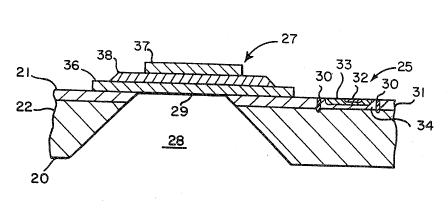
Turning now to the drawings, Fig. l i~ a diagram
which whe~tically illustrat~s the cointegration of
ac~ive dev~c~$ and thin film resonator to form an
in~grat~d oscill~tor. The integr~t~d d~vice is
ba~ed on a ~iconductor sub~trate 20 which has upper
21 and lower 22 opposed ~u~aces, which are gene~ally
planar and parall~l. A fir~t r~gion 24 formed on the
subst~ate ~0 is used for forma~ion of an active
device, in the illustrated ~bodiment a t~nch
isolated buried junction transis~or 25~ That typ~ of
transis~or i~ particularly ~uited to high fre~uency
. . ... ,
. ~ . . .
W0;~2/1~875 P~T/U~91J0~03i
7 2 ~ ~ 7 ~
applications, and thus is the currently preferred
form of active device. ~owever, other types.of
active transistor type devices can also be utilized
where desired. Juxtaposed to the transistor 25 is a
second reqion 26 which serves as a region for
formation of a thin film resonator 27. An aperture
28 formed below the thin film resonator ?7 frees a
membrane portion 19 for acoustic vibration 50 that
the thin film re.sonator can ~per~te in the
fundamen~al modec When overmoded operation is
de~ired, th~ semiconductQr substrate, or por~ions
thereoft need no~ be removed.
Referring in grea~@r d~ail to the ~ransistor
25, it is seen that a pair of trenches 30 are
provid~d-fQr isolating the active device from the
remainder of the devices formed in a doped layer 31
in the substrate~ The transi~tor 25 includ~s
additional pat~erned doped regions fo~ming an emi~ter
32 located cen~rally of the device, an intermediate
base 33, and a collec~or 34 formed in the lower
portion of ~he doped layer 31. The manner of forming
the transistor will be de~cribed in greater detail
below. ~uffice it to s~y for the moment that the
dopant impurities which form th~ bas~, emitter and
collector are d~posited by conventional techniques,
such as diffusion OI ion implantation, into the
su~face of the sub~trate, or into layers such as
epi~axially gro~n layers formed on the ~urface o the
sub~trate. Wh~n it is d2scribed herean that the .
dopant re~ions are associated with the ~irs~ surface
of the subs~rate, what is intend~d i~ a broad
description of formation o the active semiconduetor
device on tha~ surface, whether or not it includes
epitaxial grown layers, and whatever me~ns are used
for forma~ion of the patterned doped regions which
W~92/~0$75 PCT/US91/~31
8 2~7~
make up the n-type or p-type doped regions of the
se~iconductor device.
Turning to the thin film resonator, it is seen
tAat Fig. l illustrates a two terminal device
including a l~wer metal electrod~ 36, and an upper
metal electrode 37 sandwiching an in~ermediate thin
film piezoelec~ric layer 38. The metal electrodes
36, 37 as will be ~e~cri~ed in sr~ r ~etail below,
are ~ypically thin film electrodes deposited as by
sputtering or electron beam ev~poration. It is
impVrtant that the ~etallic layer forming metal
el~ctrode 36 be smooth, thin and continuous and
provide a smooth surface for receiving a highly
orien~ed ~hin film of piezoelectric material. The
piezoelectriG ~hin film layer 3a is deposit~d as by
DC magnetron spu~tering, following whiCh the upper
electrode 37 is deposited. In practicing certain
asp*cts of the invention, it is ~fficient ~o utilize
~he lower metal electrode 36 as one of the
interconnections to the active device represented by
transistor 25, and thus the meeallization layer 36
will typicaliy extend to and ~onnect with one of the
electrode~ in the active device. However, in certain
other embod m~nts of the invenkiont such as those
which provid~ an application specific IC providing
for flexibility of interconnection of individual
nts~ the ~e~onator and active devices may not be
i~ereonn~t~d at ~he formation stage.
The abil~ty to form a thin ~ilm resonator 27 and
an ae~ive device such as transistor 25 in close
juxtap~sition as illus~rated in ~ig. 1 i~ provided in
substantial ~easure by the integrated process
aecording to ~he pres~nt inven~ion. In practicing
tAe invention, and as will be described in gr~ater
~e~ail in conn~ction with ~ig. 3, the dopant layers
- W~92~87~ PCT/U~1/0~03~
for forming the active device 25 are fi~st deposited
into the top surface of the semiconductor
sub~trate. Following that, the first metallization
for the thin film resonator i~ deposited, followed by
the subsequent steps for forming piezoelectric layer
and addi~ional elec~rodes for th@ thin film
resonator. The thin film resonator is form~d on the
substrate at a time when the substrate is strong and
capable of withstanding the var.ou~ prGc~sses for
formation of the for~going elementsO Having formed
the ~hin film re~ona~or, the active device,
me~allization for the ~ontacts, and in~erconnections
if desired, the partly formed d~vice is then
subjected ~o an etching step which removes all or at
least a portion of the subs~rate ma~erial from below
th~ me~brane portion of the thin ~ resonator. In
accordance with the invention, the etching 5tep is
adapted to selectively e~ch the pure silicon of the
substra~e, whil~ being relativ~ly nonreactive to the
materials formed on th~ upper surface of the device,
such as the metallization and the ~ielectric which
are exposed on ~hat upper surf~ce. Thus, the process
steps provide for a relativ~ly non-fragile wa~er
dur ing the numerous step~ n~eded ~o deposit the
dopant impuriti~s, perform the litho~raphic steps,
etching step~, spu~tering steps and the like, then,
.la~e in the process, after ~he majority of the
proc~s step~ ar~ completed, etche away the
necessary mat~rial to free the xesona~or, but
accompli~he~ the etchin~ step in 5uch a way that the
delicate and previously for~ed resonator and active
elements are not damaged~ ~he abili~y to a~complish
that is particularly signific~nt when one compar~s
the mass of silicon which must be removed from below
the resonator with the compar~tively s~ller mass and
` ~ ~
. W~9~10875 PCT/~'~91/~31
size of the portions of the device which must be
protected.
Turning to ~ig. 2, there is shown an alternative
form of the int~grat~d device of ~ig. 1, which
incorporates a ~tacked crystal filter 30 as the thin
film resonator. A5 iS well known, the stacked
crystal fil~er inclu~es a lower electrode 31 and a
first pieæoelectric ~hin fi1m ~, an intermediate
electrode 33, ~ second piez~electr~ thin film 3~,
and an upper el~ctrode 35. In oscillator
applications, it is of~en desirable to bring all of
the electrodes 31; 33 and 35 GUt to conductive pads
(~uch as or application in an ASIC) so th~t on2 of
the por~s, i~@., the resonator ~xisting be~ween
electrod~s 31 and 33 serv~s a~ th~ input port, while
the ~econd and coupled port, the re~ona~or exi~ing
betw~en elec~rode~ 33 and 35, func~ions as the output
port~
.In a dediGated integrated oircuit, the
electrodes 31, 33 and 35 will be connect~d ~o
particular terminals in the active device represented
by transistor 25. It will al~o b~ appreciated that
in a dedicated inte~s~ted circui~, the active device
repres~nted by tran~i~tor 25 i3 inde~d only
repre~en~d by that tran~istor, and that usually a
more complex amplifier including multiple transi~tors
and other devices will be used. O~ten the thin film
r~on~tor, r~pr~ented by th~.st~cked crystal filter,
will b~ conn~ct~d in the ~eedback path of ~h~
amplifier to form an oscilla~or. ~or the detailc o
circuit int~rcannec~ions for such an amplifier,
reference can b~ made ~o th~ a~oremen~ioned Tho~p~on
et al.`applica~ion~
Turning now ts Pigs. 3a-~g, there are
illus~rated a s~uence of pro~es~ steps and the state
: . ; . .
W~92/~087~ PCT/V~91/0~31
7 ~
of formation of the d~vice as it progreSses from step
to step beginning with a raw semiconductor substrate
through the manufacture of d cointegrated
oscillator. It will be apprecia~ed that the process
steps zelate to formation o~ a single th.in film
re~onator, in ~he presen~ ins~ance a two electrode
device, which is representative of a broader rang@ of
thin film resona~ors, and a single transis~or, which
also is representative of a ~ore complex active
circuit. Thus, while the masking will be more
co~plex ~or forma~ion o device5 of the nece~sary
complexi~y, ~h~ ~equence of proc~ss steps will remain
substantially ~he ~ame.
In addition, th~ p~ocess steps ~or ~orming the
acti~e devic~ are tho~ used i~ connection with
formatlon o~ a tr~nch isolated buri~d ~unction
transistor which, as noted above, is the currently
preferred ~orm o~ high fre~uency device. ~owever,
~he inven~ion ~hould not be construed as limited to
us* o th~e Sype of device, and the illustra~ion of
the detailed steps fot formati~n of a trench isola~ed
~uri~d junction trarlsistor are simply int~nded to
illustrate ~he co~patibility ~e~we~n ~h~ conventional
integrated circuit proce~3 step~ and the 3~eps for
formation of the thin film re~ona~.or.
With ~hat in mind, turning to Fis. 3a, there is
~hown a se~iconduotor su~strate 40 having an upper
planar surface ~l and a lower pl3nar surfa~e 42 which
are ~ubstan~ially p~rallel. The substrate 40 is in
the present illustration is p~e erably a p-type
silicon wafer, app~oxima~ely lOO millimet~rs i~
thickness, with both sidec polished. An n~ spreader
lay@r ~3 and an n- type drift layer 44 are
epitaxially grown on th~ top sur~ace 41 of the
substrate. When u~ed in conn~ction with a buried
- ., ,ç
~2/10875 P~T/US91/09031
junction transis~or~ the n+ layer 43 will func~ion as
a collector, and the base and emitter will be formed
in th~ n- layer ~4.
Having thus formed the doped layers 43, 44 on
the upper surface 41 of the substra~e 40, ~he upper
surface ~over the epitaxially grown layers) i5 masked
or patterned as by photolithograp~y, to de~ine
trenches 45 which isol~t~ all of ~he t~ansi tors,
resistors and capa~itor~, a~ shown in ~-9. 3b.
Trenching is ~hen performed u~ing convention~l
reactive ion etching IRIE) techniques.
Af~er for~ation of the ~ren~hes, ~he trench~s
are then filled to provide surface planarity. Trench
refill is accomplished u~ing th~rmally grown silicon
d1oxide, or utilizing poly~ilicon and thermal ~ilicon
dioxide ~rench fill. The polysilicon refill p20ce5s
is pref~r~d because it minimize-q the overall degree
of thermal processing required. Polysilicon is
deposiked by mean~ of chemical vapor depo~ition in an
epitaxial re~c~or. ~aving re~tor~d surac~
planarity, a mask i~ formed over the upper suFface
and patt~rned by photolithogr~phy to defin~ ~inker
aperture~ ~8 (~ee Fig. 3b~. The sinkers 48 are
filled, ~or @~ple by conventional liquid phase
epitaxy, with n~ ma~e~ial intended to provide a law
re~istivi~y ~onnection to the layer 43 which s~rves
as th~ traasi~Sor collector.
Fig~ 3c ~h~n illu~rate~3 the sub~equent tep of
forminq guard rin~s SO in the base . region of the
transis~o~. The guard ring, as is-well known,
enhances high ~requerlcy ope~a~ion in ~his type of
device. The ~ings 5Q are ormed by diffusing of
p-type mat~ial into ~he sub~trate ~hrough an
appropriately d@l ined ma~k. A low re~ ivity base
region S2 is also provided by difusing p-type
.
-
WO~ 875 PC~/US91/~031
~3 ~7~
material of higher concentration than in ~he guard
rings into the base re~ion 52, as illustrated in Fig.
3d. The masks or guard ring diffusion as shown in
Fig. 3c, and main base diffusion as shown in Fig. ~d
can be similar, with a common portion deÇining the
exterior outsid@ of the ring, an in~ermediate central
portion being pr~sent. for definitioq o~ the quard
rin~s, then removed during the main b~e dif~usion.
H~ving form~d the base and the guard rin~
structure illustra~ed in Fig~. 3c and 3d, an emit~er
difusion is ~hen performed ~s further ill~stra~ed in
Fis. 3d. ~n appropriate mask formed in ~n insulator
l~yer 5~ is utilized to expose a central por~ion of
the base region 52, and n-type dopant impuritie~
difus~d in~o ~he unma~ked central portion to form an
n-type emitter region 54 centrally o~ the previously
formed p-~ype ba8e region. The emitter diffusion is
preferably ~ai~ly shallow to provide an active ~ase
region thickne~ b~low the emi~ter region of about
.25 microns or le~s.
As is al~c shown in Fig. 3d, the insulator layer
53 ~hich had b~n pa~terned ~o form the emitter 54 i~
further p~ttern~d and etched to form b~s~ vias 56
allowing ele~trical cone~ct with th~ base xegion
52. Thus, as the p~rtly completed device exi~ts in
Fig. 3h, all of the patterned regions ~or the
~e~icondu~tor are dop~d with the ~pprop~iate
conductivi~y impu~ities and the devic~ i~ prepared to
receive met~lliz~tion far connee~ion ~o ~he various
electrodes of the active device, in the illu~trated
embodiment to the ba~e, emitter and collec~or of the
transistor. Thu , the emitter 54 is exposed ~hrough
~he aper~ure in in~ulator 53 which allowed th~
emitter difFusion. The b~se is expo~ed through vias
56 formed in the insulator layer 53. And the
WO ~2/10875 PCr/U~gl/09~131
14
collector is exposed via sinker contacts 48.
In accordance with the invention, complemen~ary
process steps are then utilized to form the thin f ilm
resonaeor in juxtaposition with the partly ~o~m~d
active semiconductor device. Thu~, in the eatemplary
process of ~ig. 3, Pig. 3e illust~aees the deposition
of a first collductive lay@r 60 which, in that
illu~trat~d ~mbodim~nt, serves not only as the lowe~
electrode for th~ thin film reson~tor, QUt al~o as
interconnectins m~talli2atiGn with the active
deviceO Thu~, it is seen that the layer 60 is
deposited in a re~ion 62 in which th~ ~hin film
resonator will be ~ormed, and also extends to form
electrical contae~ with the sinker 48 and thus is in
electrical contact with the colle~tor of the active
device. It i~ noted that the conn~ction to the
collector i~ only exemplary, with Pig. 3 being
in'cend~d to illu~trate the ability to in~erconneot
the device~, rather than the specific t~rminals which
ne2d to be i~ ~erconnected in a partirular
configuration. It will be apparent that by
appropriate air bridge ~echnique~t ~or example, the
metallization 60 c~n be connec~ed 'co any of the base
or emitter con'c~et~ o the trhn~i~tor if desired.
In utilia:ing the metal l~yer 60 a~ both an
elec~rod~ of the thin f ilm resonator a~ well as a
eonductor conn~cted to the semiconductor device, it
is; de~irable to utilize silicon doped aluminum ( 1%-
2%) to enhance l:he fllnction. of the conductor as a
con~act metal. The metal layer i~ pre~rably
depo~ited by RP sput~ering or ele~t~on b~
evaporation, RF ~pu~tering ig desirable because it
achieves better contact with the active region of the
semiconductor device.
Having deposited the me~allization S0, the me~al
: ,
:.
W~g2/lQ~75 PCT/US~ 31
lS '~
is then co~er~d with a photoresist, patterned and
etched to form the metal layer into the desired
pattern. The d~sired pattern will include a
comparatively large area (e.g., 400 by 400 micron
rec~angular area) as the resonator section of the
thin film reson~tor, as well as thin interconnecting
conductors to the active d@viee. When formed as an
ASIC, the metallization can also inolude conven~ional
contac~ pads.
After the photoresist is stripp~d rom the
device in the condition illustrated in ~i~. 3e, the
proc~s~ prooeeds to the 5~age illustrated in ~ig. 3f
which include the formation of the thin film
piezoelectric layer 62. The piezoelectric layer 62
i~ preferably of ~lN deposit~d in an oriented film by
DC sputtering. ~n available ~chnique for patterning
the AlN l~yer over the lower metallization 60 is by
sputtering through a fixed ~k. ~owever t in
practicing ~he present inv~n~ion, it is presently
preferred ~o use a di~lectric lif~off process for
patterning of th~ ~lN piezoelectric layer.
In utilizing the dielec~ric liftoff proce s, an
initial layer, which will serve as a sacrificial
layer in the dielectric lif~off proce~, is ~irst
deposit~d. It i~ currently prefYrred to utilize zinc
oxide as the sacriicial layer and to deposit tha~
m~erial by ~putter d~position using ~ DC
m~gn~tron. A zinc t~rget is u~ilized in an oxyg~n
pl~ma to depo~it a Z~O l~yer, pr~ferably about 5
microns in thickn~s, over ~he en~ire upper surface
of the deviceO Th~ zinc target i then removed and a
silicon target put in its place ~o deposi~ about ~`
1000 A of sllicon dioxide over the ZnO layer. A
layer of photore~ist is th~n ~pr~ad over the silioon
dioxide and photolithographically patterned to creaee
,
9~ 7~ l 6 2 ~ ~ 7 ~ ~ ~ P~T~US91/0~031 l l
windows in which the aluminum nitride is to be
formed. The silicon dioxide is then etched, u5ing a
buPfered hydrogen fluoride solution. ~ollowing
etching o~ the window in the silicon dioxide, the
zirac oxide is then el:ched using hydrochloric acid.
The double ~tching leave5 a . helf of silicon dioxide
ov@r a cavity in the ZnO whiCh exp~es the aluminwn
bel ow the zinc oxide layer .
~ avin~ ~huS opened windows over the aluMinum in
~he area~ in which the piezoelectric resonator
mat~rial is to b~ deposited, the device is r~turn~d
to the ~C m~gnetron. Usin~ a highly pure alumirlum
targe~ (g9.999~ purity) in a nitrogen ~tmosphere,. a
very pure thin and smaoth layer of aluminuDrl fli~ride
is deposited, approxi~ately S microns in thickness.
After depo~ition o the alu~inum ni~ride film,
the wafer is then soaked in dilute hydrochloric acid
which tends to dissolve the ZnO~ That proc~s i~
conventionally known as dielectric liftof. In the
present in~tance, the ~luminum ni~ride in re~ions
other than the window is r~mo-~ed, leaving an aluminum
nitride thin film ~epo3it~d oY~r and in intimate
contact with ~he ~luminum in th~ region which had
been d~fin~d ~y the window. The par~ially completed
device at this s~age i5 illu~trat~d in ~ig. 3f.
The device is ~hen returned to a ~urther
photolithographic proce~s for ~ormation of an upper
ele~trode 64. FigO 3~ al30 shows the uppe~ elec~rod~
a8 d~po ited over the aluminum nitside piezoel~c~ric
layer 62, but not showing any ex~en~ions of the
metallization for interconnection ~o the active
deviees. ~owever, it will be apparen~ ~h~ the upper
~le~rod~ will be brought out to cont~ct~ (no~ shown)
or in~erconnections to the activ~ device~ a~ will be
determined by the particular circui~ configuration of
. . ~.
W092/1~5 . ~CT/USgl/~31
' 17 . '~ ~ 97 ~
the oscillator being constructed~ The showing of
Fig. 3f is simply intended to illustrate the process
step for forming the upper electr.ode 64 and
piezoelectric layer 62, rather than ~he details of
its shape.
The forma~ion of the upper meeallization is
pre~erably by a liftof proce~s. Having thus
pattern~d and depQslted the di~lectric layer, the
upper metalliza~ion is depo5.ted by a ~itable
prQcess such as electron beam ev~p~ration. The wafer
wi~h d~positgd upp~r met~llization is then soaked in
a bath of ~cetone to dis501ve the photoresist and
li~t off th~ metal in all but the desired areas.
~ ig. 3~ illustrat~s th~ waf~r at this stage and
includ~g the a~tiYe device repr~nted by ~he
transistor, the re~on~tor d~viee represented by the
~hin film re~on~tor, and certain of the
interconnection~.
In accordan~ with the inv~ntion, when ~he ~hin
film r~sonator requires a ~embran~ in the area 62,
that membrane i5 then formed by ~ubse~uent process
s~eps which selectively remov~ the qilicon substrate,
bu~ do not attack the ~ctive deviee, the thin film
resonator, or th~ in~erconnecting metallization.
Fig~ 3g illus~rates th~ patt2rni~g of an aperture 66
on ~he ~cond surface 42 o~ the ~ubstra~e 40 and the
etching of th~t ape~ure in th~ area 62. It is ~een
th~ the etchin~ proceed~ until ~he low~r alumin~
layer 50 i~ rQached, with the ~luminu~ layer 60
serving ~ an ~t~hant ~top to def ine a thin membrane
67 comprising the metallization layers and
interm~diat@ aluminu~ nitride ilm forming the
ieesona~ing device of th~ thin film r~vnator.
Further details of the e~ohing process will be
provided below (as well as additional detail on ~he
W~92/10875 P~T/VS91~031
18 2~9~ ~ 7
sputte~ing of the piezoelectric film) to bet~er
illus~rate the practice of the present invention.
However, at this point, it will be noted that the
elements which are nec@ssary for a~ integrated
oscillator have been formed in an inte~rated process
on the same semiconductor substra~e and in close
juxtaposition. There i~ little requirement in the
proce~s steps which form the respective d~vices to
require gr~at se~r~ion b-tweer the devices,
allowing use of two macron de~ign rules for ~he
in~egrated device. The diffu~ion profile~ required
for high fr~qu~ncy tran~i~tor5 ~re considerably
easier to obtain in ~he illu~t~a~ed proc@sR because
of ~he lack o~ a p+ me~br~ne needed ~or ormaSion of
the thin ilm r~nator according to p~ior
techniques. As will be appEeciated rom an
examina~ion o ~iy. 3, in that proc~s flow virtually
all device proces~ing is completed except for the ~op
side circuit defining ~etallization before the thin
film resonator for~tion steps are initiated.
Fig. 4 is a diagram illustra~ing an application-
specific inSegrat~d circuit (ASIC) palette or chip
lO0 ~hich is form~d from th~ p~ocess according to the
presen~ invention for cointegr~ting active devices
with th.in ilm re~ona~ors.
ASIC ~hip lO0 includ~ qeveral thin film
ra~on~ors lOl, trench isolated npn tran~istor~ lO~,
and r~ tor~ 103. ~5IC chip 100 also include~
digitally-~calcd MOS capacitors lO4 ha~in~ fusible
links fo~ tuning if nece~ary, pnp transistors 105,
and inductors lO6. The rem~ining componen~s on ASIC
ohip lO0 comprise a se~ies of t~t pa~t~rns used ~o
perform ~arious tes~s on t~e components of ASIC chip
lO0. These t~st patterns ar~ not shown in detail,
~ ^92/10~75 PCI/US91/~031
19 f~ 0 9 7 ~
but area 107 of the ASIC is indicated as being
reserved for such as te~t patterns.
~ SIC chip 100 shs~wn in Fig. 4 includes a
relatively large number of compc:nents so that a
single ASIC chip can be used to design a wide variety
of cointe~rated oscillators, band pass amplii~rs, or
o~her deYice~ operable at high f re~uencies . ASIC
chip 100 i~ highly versatile, and provides all o the
compon@n~s nece3~ary ~ desagn an~ f~bri~ate numerous
high f requ~ncy devices, and therefore eliminates the
n~ed or a~ditional microelec'tronic eh~ps in order to
complete a particular d~sign. Thus, ASIC chip 100
o~n be used to de~iyn oscillators and ampllier3
re:auiriny v~rying deg~ees o~ chara~teristics such as
tunabili~y, s~ability, an~ power ou~p~ut~ A
particular coin~egrated oscillator or o~cher det~ice
can be easily realized with ASIC chip 100 by maqking
a top metallization layer a~ross the ASIC chip to
in~erconnect. the various components need for a
particular de~ign.
. Fi~. 5 i~ a block diagram showing a basic
oscillator configura~ion 13û. Fig. 5 is included to
illustr~te the versatility of A51C chip 100, and to
demonstrate th~t it can be u~ed to encompass a wide
varie~y of d~3~gns for high fr~quency oscillator~,
am~plifier~ or othe~ devices. For ~x~mple, oscill~tor
eonfigur~tion 13û include~ an activ e device 131 and a
f~edl~ack l~ ck 132, which includes a~ least one o~
the thin ~ilm re~onators 101, connect~d in a loanner
to d~monstrat~ that series resonance can be realiæed
with A5IC ~hip 100. Further, fe~dback blo~k 133 is
connect~d in a manner ~o demonstrate that parallel
resonarlce can al~o be r~aliz~d with ASIC chip 100.
Oscillator oonf igura~ion 130 also includes feedback
blocks 134 and 135, and load bloek 136 to further
W092/l0875 PCT/US91/~3l
~977~
illustrate the versa~ility available from ASIC chip
100 .
Pig. s also illustrates that ASIC chip 100
includes all of the components neoessary to complete
a particular cointegrated high frequency
oseillator. Because of the close int~gration and
juxtaposition of the various ac~iv~ devioes, ~hin
ilm resonators~ and ancillary devices ~uoh as
resistors, c~p~citors and ~nductors, a m~tallization
layer can b~ d~posited on ASIC chip 100 which
in~erconn~t~ ~he component~ needed for a particular
design. Fo~ example, in Fig. 5, active device 131
repre~nts any o~ the n~ber of tran~istors oÇ ASIC
chip 100. ~urther, feedback blcck 133 ~hown
connec~d in par~llel to active device 131 can be
provided by one o~ ~he thin il~ re~onators of ASIC
chip 100 interoonnected wi~h any ~equired ancill~ry
devices neoe~sary to comple~e the particular desi~n
of the cointe~r2ted oscilla~or.
The ~ignificanoe of providing an ASIC in
technology previou~ly implemented by hybrid circuits
~hould now be appr~ci~ted. In the p~, the thin
ilm resonator h~d typlG~lly b~en for~ed in a
separa~e proce3 regui~ing the high frequgncy
oscillator to be fo~m~d as a hybrid device. In
~ccordance wi~h ~h~ inven~ion, ~he process steps for
for~ing th~ activ~ d~vice and th~ thin film resona~or
ar~ rend~r~d ~uf~ici~ntly compa~ible to not only
allow ormation o~ a ~pecialized integrated cir~uit
inclu~ing an a~plii~r and the thin film resona~or,
but exsending so ~ar as to provide an ASIC including
mul iple such devices. Thus, ~he device o ~ig. 4
shows a plur~lity o ~hin film resona~or~ in~egra~d
wi~h a larg~ plurality of transistors ~nd other
ancillary deviGes, significantly advancing the
.: :
W~;~ 92/10875 P~/US91/û~031
2 l ~ t~f
technology well beyond prior capabilities of hybrld
circuits to ~arry the two types of devices. Thus,
where a hybrid circuit might previously have been
requi red to provide the neces5ary high f requency
crystal controlled stability, now it is possible
uslnq the ASIC of ~ig~ 4 to n~t only E~rovide those
design requirements in a sin~le coin~grated circuit,
but to provide the ability to design a wide variety
of electrical charac~:eristics into that circuit which
is ~hen integrated by simply designing an
in~erconneoting ma~k layer~
In th~ proce~s de~cription of ~igs. 3a-3g,
par~icular mention was made of the selective etching
step for xemoving substra~e ~aterial from b~low the :~
membrarl@ of the thin f ilm re~onator, and also the
proce3s 3tep for dielectri~ liftoff in co~nection
with patterning th~ dielectri~ layer of ~he thin ~ilm
re~onator. Additional information will now he given
on those two process S~:ep5.
In re~noving sub~trate material f rom below the
membrane ~f th~ thin film resonator, an anisotropic
etching proc@~ employ~d which etches along the
llll) çry~t~l axeo from the rear ~ur~ace 42, with the
first me~l layer 60 3erving a~ an etchant stop. The
rear ~urface 42 o~ the ~ub~tE~te i9 ma~ked by
~ult~bl~ loat~riaïs ~uch as a ctlicon dioxide layer
appropria~ely p~t~rned u~ing standarà techniques to
fo~ window~ in th~ ~r~ where the membrane i~ to be
formed. Th~ windows ~an be aligned with the devices
form~d on the upper surface 41 as by using inf rared
al ignment techniques O
The etching ~olution which has been found to be
sel~ctive to 5ilicon while ~ub~tan~ially nonreactive
to the alu~inum nitride and aluminum metallization is
a solu~ion of hydra2irle and quinoxaline preproces~ed
.
- W~92/1Q875 PCT~US91/0~03~
22 2 ~ ~ r~
as will be described below. A desirable olution
consists of proportions comprising approximately 850
millilite~s of hydrazine hydrate (85 weight percent
solution)~ 650 milliliters of deioni~d water, and
approximately 1 gram of quinoxaline which had been
vacuum distilled to r~move oxide oontamination. The
solution is heated to a reaction tempera~ure of about
108C, its boiling point. Once the reactor i at
temperature, ~reproc~ssing i5 ~om~c~d by imm~rsing
a silicon wafer for a short interv~lj approximately 5
~inutes, for ex~ple. The wafer i~ then r~mov~d and
the solution is allowed to pr~condition for a period,
pr~ferably at le~st 3 hours. The l~ngth of the
interv~l of preconditioning is not limited to three
hou~, and ind2ed once a solution i~ employed to etch
integrated devices on ~ilicon, tbe preconditioning
inde~d c~n extend in time for substantially beyond
three hour~ with the solution r~maining selective to
sili~o~.
~ aving preconditioned the etching solution by
~rea~ment with silicon and aging, waferç of ~he type
illust~a~ed in Fig. 3j are then i~m~r3ed in the
heated ~olution ~or ~tching. The ~olution is
selectiv~ to ~ on and thu~ will remove tho silicon
su~strat~ in th~ area 66 defin~d by the windows while
not ~t~cking th~ ~e~allization or dielectric layers
~n the upper ~urf~ce of the device. In ~ome c~se~,
it ~ay b~ de~irable to pas~iva~s the upper surf~ce
with a mat~rial such as ~ilicon dioxide which is not
reac~ive to the etchant. When etchin~ is completed,
as will be det@rmined when the et~hing reaches the
aluminum layer 60 to which the etchant is
nonreactive, thus ~erving as an etchan~ stop~ the
wa~er is then remov~d ro~ the etchant solution,
~ . - -
:. .:.. . ..
-, ~
--W~ g~ 7~ . PCrlU~g~ 31
23 ~g77~'~
rinsed with deionized water and dried, such as in a
stream o~ nitrogen gas.
The significance of the foregoing etchan~
process will be appreciated in that it provides a
mechanism for allowing formation of both ~he
semiconductor ~evice and the thin film resona~or on
wafers which can be readily h~ndled in the ordanary
semiconduc~or fabrication proces~ flow, follow2d by a
sub8equent etching st~p for formatlon o~ thin film
resonator mem~ran~ by a sel~ctive ~tching prooess
which remove~ the silicon to for~ the membrane
wi~hout attacking the ~lements pr~viou~ly put in
plac@ which make up ~he d~vices.
~ s noted above, the aluminum nitride film is a
highly ori~n~ed and very pure film for~ed by ~putter
deposition. In forming that Eilm, it h~5 been ~ound
desirable to utilize peciali2ed technique to account
~or the relatively long depo~ition times which are
required. Tho~e techni~u~ involv~ u~ilization of a
DC magne~ron reactive sput~ering sys~em which in one
implem~nta~ion uses an 1800 wat~ 600 volt DC power
supply as She cur~nt ~ource. Typic~l operating
parametezs ase 5 mTorr pre~ure, 0.5 amp current with
a vol~age drop ~cro s ~he nitrosen pla~ma of abous
350 voltsO ~ho ~e~iconduetor ~ubstr~te is poRitioned
oppo~ite a v~ry pure ~99.999~) alumlnum target. A
ring po9ition~d between ~he sub~trate and target acts
an anode ~o a~si~t in co~taining and ~tabilizing
~h~ nitrogen pla~m~. The riny typically has a
potential of about 4~ volts. The plas~a contain~ a
large numbe~ of positively charged iolts which
accelerate into th@ targe~, knocking loose atoms of
alu~inum, The aluminum atoms then ~raverse the
chamber and deposit on available surfac@s. ~hen
being deposite.d in the presence of a reactive gac
` W~ 92/1~B7~ PCT/US91/0~031 ll l
24
such as nitrogen, the aluminum atoms will form
comp4unds, in the present instance aluminum nitride.
As noted above, the aluminum nitride film is
preferably about S microns iA thickness in order to
provide resonator respons~ at about l G~z. At
optimum deposition parameters, approximately 4 hours
of deposition are required. In addi~ion, the crystal
grain growth must be Qrient~d in order to provide
good piezoelec~ric response.
Using those relativ~ly long depo~ition time ,
the chamber of the magnetron b~come~ electrically
insulated, which can r~ult in i~purities being
dislodged from the chamb~r and deposited in the
aluminum nitride fil~ orming on ~he ~miconductor
substr~eO
In accordance with thi~ aspect of the invention,
during the relatively elong~t~d deposition procedure,
a layer of aluminum me~l is periodically teposi~ed
oves the aluminum nitride ~uildup on the chamber to
prevent contamina~ion of the ~lN film being deposited
on the semicQnductor substrate. This is acco~plished
by chan~ing ~he.r~activ~ gas in th~ chamber to argon
in place o~ the nitrcg~n for a brief p~riod. To
prevent the wafer from being coated with the aluminum
during this periodic "cleansing" pro~e~s, a shutt~r
i~ moved into place over the subs~rate to act as a
~hield. Thus, at periodic intervals, such aq about
30 ~inu~, du~ing the ~epo~itlon of the alu~inum
~itride, the shutter is closed and the nitrog~n
~mosphere replaced wi~h argon, to coat the walls and
other elements of the r~a~tor with an aluminum
film. The argon i5 then removed and the nitrogen
a~mosphere returned, following ~hich ~he shutter is
opened and aluminum nitride deposition con~inued,
until the r~quired thicknes- has been built up. The
,
.
W092/1n875 25 ~97,~,7 PC7/1'591/0903~ l
alternating oÇ AlN and Al deposition (with shutter
closed during Al deposition~ is repeated until the
required amount of AlN has been deposited onto the
semiconductor substrate. This procedure has been . ~`
found to produce sub tantially purer ~alms than has
been available using conventional sputtering
techniques.
This disclosure has provided substan~ial de~ail
on a number of related proc~ss~s which ~re u~ilized
in the formaSion o~ active semieonductor devioes and
thin film re~onator device5. Th~ details of ~he
proc~ss are impor~a~t, but it is of p~rticular
ignificanc~ that the proce~es are all
cointegratable for forMation o~ an integrated
oscillator device which of nece~ity includes bo~h
active el~ents and one or ~ore thin film
re~onators. The proce~ steps unique tG the
ormation of the thin ilm resona~or are adap~ed for
forming high quality resonators, freeing the membrane
for vibration, and all in a manner which is entirely
compatible wi~h and not de5truotive of the active
semiconducto2 d~vices which are formed in ~he
int~grated p~oce~.
It will thu~ b~ appreciated that what has be~n
provided i5 an inte~rated process for formation o~
high ~requoncy oscillat4rs including both re~onators
and active devices, and the resulting device.