Note: Descriptions are shown in the official language in which they were submitted.
7 o 9 7 7 2 g
POWER CONTROL DEVICE WHEREIN A BIAS VOLTAGE
IN LEVEL DETECTION IS GIVEN A CONSTANT
DIFFERENCE FROM A DETECTED VOLTAGE
BACKGROUND OF THE INVENTION:
This invention relates to a level or power control
device for use in digital modulation accompanying an
amplitude variation, such as in ~/4 quadrature phase shift
keying (QPSK) modulation.
Various level control devices are already known for
use more in general. According to one design, an
intermediate frequency (IF) signal is preliminary mixed
with a local signal into a radio frequency (RF) signal for
supply to a prior-art level control device. In an improved
level control device, an IF signal is supplied directly to
the level control device. The improved level control
device produces an RF signal with a controlled level.
2 2097729
Meanwhile, conversion of analog communication to
digital communication is in rapid progress recently.
Digital modulation with an amplitude variation is widely
applied to communication networks. For example, ~/4 QPSK
modulation and demodulation is becoming into practical use
in a mobile telephone and/or other communication network.
In general, a level control device is supplied with
a device input signal and produces a device output signal
having a controlled or predetermined output level. For use
in digital modulation accompanying an amplitude variation,
a novel level or power control device is invented b~ the
present inventor. This novel level control device will be
used as showing the state of art on describing the present
invention.
In the manner which will later be described in
greater detail, the novel level control device comprises a
variable attenuator responsive to the device input signal
for producing an attenuator output signal having an
attenuated level, a level detecting unit for detecting the
attenuator output signal to produce a detected signal
having a detected voltage related to the attenuated level.
Supplied with the detected signal as a generator input
signal and comparing a digital value of the detected
voltage with a reference value, a control signal generator
generates an attenuation control signal having an
attenuation control level.
B
209772g
More in detail, the ~oPtrol c.ignal gener~or
co~pris~s an A~ converter ~or ~onvertin~ ~he deteoted
voltage to the digital value Comparing the ~i~ital
~alue ~i~h the referen~e value, a processor produces a
digital control signal having a digital con~rol value.
Con~ertin~ the digital con~rol value to an analog value,
a DA converter p~oduces the attenuation control ~ignal
with ~he ~n~lo~ val~e u~ed as ~he attenuation cont~ol
level.
Controlled by the attenu~tion con~rol signal, the
variable at~enua~or enables use o~ the a~enuator output
signal as the de~ice outpu~ signal. T~e referen~e value
is readily determined by the controlled outpu~ leve~. It
is possi~le to u6e whichever o~ ~he IF and the R~ nals
1~ a~ the device inpUt si~nal.
When used in time division multiplex (TP~)
- modula~ion, the novel level control device is very
effecti~ely operable. I~ i~ kno~n tha~ the TDM
~odulation is desir~ble in effectively using ~hannels
2~ ~he novel level co~trol de~i~e, however, has a
fe~ defect~ when such ~ level co~t~ol devioe should be
reliably opera~le, namely, ~e operable s~ably and
precisely or correctly. More par~icularly, opera~ion of
the novel leve~ contr~l device ~ecome~ unst~ble and
incorrect when ~he controlled output lev~l is low,
typically, when the con~rolled outp~t level is no~ higher
than plus 10 dBm.
2~97729
One o~ ~he defects is such that the level eontrol
is unstable ~ainst ~ varlation in ~he a~b~ent
tempera~ure. The 1evel dete~ing unit include~ a
detector diode for detecting the ~ont~olled output level
which i~ derivea ~rom the attenuated level. ~hen ~he
controlled output ~e~el i6 low, the detector diode ha~ a
high internal resista~ce and becomes excessively
~nsitive to the ~emperature variation.
In such a level detecting unit, ~he detec~o~
diode is usually supplied wi~h a con~ant bias current
with a bias vol~age. When the controlled ou~put le~el is
low, Sl~e detec~ted voltage is subjected to an
objectiona~ly ~ide variation by a slight ~ariation in the
controlled output level.
1~ Another defect is an appre~iable influence caused
to the ~t~enuation ~ontrol level by con~ersion error~
ine~itable in operation o~ ~he A~ and ~he DA ~onverters
When the controlled o~tpu~ level i8 lo~, the conversion
errors are not negligible as compared with a li~tle
~0 varia~ion in the detec~ed ~oltage.
The vari~ble at~enuato~ ~sually comprises
attenuator diodes and has an attenuation characteristio
whi~h i~ noniinear relative ~o ~he attenuation control
level~ W~e~ the controlled output level should ~e low,
2~ the variable a~tenuator m~st gi~e a gre~t amount of
~t~enuation to the deviee input signal. ~o~
purpose, ~he attenuation control le~el mu~t be given a
small value. ~onsequently, i~ ag~1n results ~hat ~he
2097729
.
con~ersion errors are no~ ne~ligible when compared with
this small value of the at~enuation c~ntrol level.
S~MMARY OF THE I~ENTIO~:
It is consequently a p~inripal o~ject of the
present in~ention to provide a level cont~ol d~vice which
i~ for u~e in TPM modulation ana is stably and pre~isely
operable
It is another prir~c:ipal object of ~his lnventio~
to provide a level control devl~e which i~ of the type
described and which is stable a~ains~ a ~ariation in
~emper~ure.
It is a subordinate o~je~ of ~his invention to
provide a level control device which i~ of the type
described and which is operable with lit~le ad~ersely
affe~ed ~y a conver~ion error between analog ~nd digital
value 5 .
Other obje~ of this inven~ion will be~ome clear
the description proceeds.
On se~ing forth the gist of an aspect of thi~
invention, it is possible to understand tha~ a level
~ontrol aevi~e prod~ces for use in ti~e aivi~ion
~ultiplex modulation a device output signal in response
to a de~i~e input signal ~ith the device outp~t signal
given a controlled ou~p~t level and co~prises: (~) a
va~iable a~tenuator resp~nsive to the device input signal
fo~ producin~ an attenuator outpu~ signal h~ving an
attenuated level, (~ a bi~s current generator for
~enerating ~ bias current, (c~ level de~ecting mean~
6 2~9 7729
~ontrolled by the bias ~urrent ~or de~ecting the
attenuator ~tput signal to produce a de~ee~ed signal, ~o
develop a ~ias voltage, and to give ~he dete~ed signal
alterna~ingly a dete~ed voltage related to ~he
a~tenua~ed le~el and the bias voltage, (d) a contro~
signal generato~ responsive to a genera~or input signal
and a reference value for generating an at~enuatioA
control sig~al having an ~ttenuation con~rol level, and
(e) attenuation ~ontrol signal supply means for supplying
the attenuation control signal to the variable a~tenuator
to enable use of the attenu~or output signal as the
device output signal.
In ~ccordance with the aspect bein~ described,
the above-understood le~el control devi~e is
cha~aoterisea as fol~ows (A) The bias current gene~a~or
generates ~he bias cu~ent ~o give the bias volta~e a
su~stantially temperatu~e independen~ difference from the
detec~ed voltage irre6pective of a ~e~perature ~a~iatlon.
( ~ ) The oontrol signal generator uses the detec~ed signal
~o as the generator inp~t sign~l to ~onve~t the dete~ted
vol~age and the bias volta~e ~olle~ively to a
substantially tempera~ure independen~ digi~al value and
compares the digital Yal~e with the reference value to
derive an anaiog ~alue for use as the attenuation ~on~rol
~5 level
On setting forth the gist o~ a differen~ a~p~t
of ~hi~ invention, it is possible to underst~nd that a
le~el oontrol de~i~e produ~es for use in time dî~ision
- 2097729
m~ltiplex modulation a device outpu~ sign~ in respon~e
to a deviee input sign~l wi~h ~he devi~e outp~t ~ignal
given a oont~olled output level and comprise~; (a) a
variable at~enuator responsive to the device inpu~ signal
f~r producing an attenuator output signal ha~ing an
attenuated level, (b) a bi~s current generator fo~
gene~ting a bias ~urrent, (c) level detecting ~eans
contr~lled hy the bias cUYrent for detecting the
attenuator o~tpu~ ~ignal to produce a de~e~ted sig~al, ~o
develop a developed bias voltage, and to giYe ~he
detected ~ignal ~lternatingly a detected volta~e and the
bias voltage, (d) a ~ontrol signal generator responsive
to a genera~or inpu~ signal and a reference value for
genera~ing an attenuation con~rol ~i~nal havi~g an
lS ~enuation control level, and ~e) at~enuat~on con~rol
signal supply me~n~ f o~ pplying the attenuation control
signal ~o the variable a~tenuator to ena~le use o~ the
attenuator ou~pu~ ~ignal as the device output 6i~nal
In accordance wi~h the different aspec~ of this
inven~ion, the a~ove-unders~ood l~vel control device is
char~te~ised a~ follows. The leve~ ~on~rol deviGe
further comprises: (A~ a gain varia~le amplifier for
amplifying the d~tected sign~l wi~h a ~ariable ~ain ~nto
an ~mplifier output si~nal to give the a~plifie~ ou~put
signal alternatingly an ~mpli~ied volt~ge related to the
detec~ed voltage and an ampli$ied bi~s volta~e rel~ted ~o
~he dev~loped bias voltage, and (B) a g~in controller
responsive to a devi~e ~ontrol si~nal for controlling ~he
2097729
varia~le gain. ~C~ The bia~ current ~enerator ~en~r~tes
~he bia~ e~rrent ~o give the developed ~ias volt~ge a
su~stantially ~onst~nt difference from the de~ected
voltage irrespe~tive of a temperature v~riatlon. (D) ~he
con~rol signal generator use~ the amplifier output signal
as the g~nerator inpu~ signal to con~ert the amplified
volta~e and the amplified bias voltage collec~ively to
substantially temperature independent di~i~al val~e an~
compare6 the digital value ~ith the reference value ~o
derive a digit~l control ~alue, to produce a processor
output signal havlng a digit~l processor outpu~ value
propor~ional to the digital ~on~rol val~e, and to ~onvert
the di~ital control value ~o an analog signal for us~ as
the at~enuation ~ntrol signal, ~e ~ontrol si~nal
genera~or thereby supplying the processor o~tput signal
to the gain cont~ol~er as the device ~ontrol signal.
BRIEF DESCRIPTIO~ OF T~E DRAWI~G-
~ig. 1 is a blo~ diagram of a level ~o~trol
device known by ~e present in~entor;
Fi~, 2 schemati~ally shows a ~har~cteristic of
level detector u ed in 5u~h a level control deviGe;
Fig. 3 is a s~hematiG represent~tion of ~
~hara~teristic of a variable a~tenuator for use in a
le~el control device o~ the type ~éing illustrated;
~ig. 4 is a block diagra~ of a level ~ontrol
device according to an em~adiment of ~he instant
in~en~ion;
2097729
Fi~ 5 s~hema~ical~y shows a rel~tionship between
a dete~ted voltage and a bias voltage used in t~e le~el
~ontrol devi~e depicted in ~ig. 4; and
Fig 6 is a flo~ chart fo~ use in des~ribing
operation of the level ~ontrol devi~e illustra~ed in
Fig. ~.
~ ESCRIPTIO~ OF THE PREFERRED EMBOnIME~T;
Referring to Fig 1, a~tention ~ill be dire~ted
first to a level or power control device ~hi~h is
descri~ed heretobefore as a novel level con~rol device.
Thi~ is in order to facilitate an unde~standing of ~he
present inven~ion. It will be surmised ~hat the level
con~rol device is for u~e in a time division multiplex
(TDM~ modulation system. T~M ~odulation is digital
modulatlon wi~h an amplitude Variation and is t~p~ally
~/4 quadratu~e phhse shift keying (QPSK~ modul~tion wi~h
TDM
In ~ig. 1, the level ~ont~ol device i6 supplied
with a device input signal S(1) for u~e in the T~M
mod~lation 6ys~em and produces a devi~e outpu~ ni~na
S(o) ~hich i~ ~ rAdio frequency ~RF) signal havin~ a
controll~d or prede~ermined ou~pu~ power o~ level It is
possi~le to use whichever of an intermediate frequen~y
(~F) signal and an RF ~ignal as the deviGe input signal
Merely for convenien~e of the descrip~ion, it ~i11 be
presumed througho~t ~he follo~ing that the device input
signal is an IF si~nal unless it is spe~ifically
mentioned that the ae~i~e input 6ignal is an RF signal.
2097729
Supplied wi~h the devi~e inpu~ nal, a ~ariable
a~e~ua~or 11 prod~ces ~n atten~ator o~tpu~ si~al having
an attenuated level. An up converter 13 comprise~ a
local oscillator (not shown) for generating a lo~al
signal and a ~i~er tnot sho~n) fo~ ~ixing ~he a~tenuator
output signal with the lo~al signal into ~n RF
intermediary si~nal ~ po~er ~mplifier 15 ampli~ie~ the
RF intermediary ~ignal in~o an amplified signal of an
ampli~ied le~el Inasmueh as the amplified ~ignal is
pr~duced in this manner, t~e amplified level is related
to the attenuated level.
The amplified signal is ~oupled to a level
detec~or 11 in the manner whi~h will presently be
described The level dete~tor 17 detea~s the ~mplifled
signal and prod~çes a detected signal havin~ a de~ected
voltage related to ~he a~plified level and consequently
to the at~enua~ed level.
More particula~ly, ~he level detec~or 17
comprises a first ~apaci~or Cl supplied ~i~h the
amplified signal. A detec~o~ or fi~S~ diode C~l ~nd a
secona capacitor C2 are connected ~n se~ies ~et~een the
fir~ capaci~or and g~ound to serve as a re~tifier for
produ~ing a h~lf wave rec~ified signal. ~ poin~ o~
~onne~tion be~ween ~he de~ector diode ~nd the se~ond
capacitor is grounded thro~h a series eonne~tion of a
fi~s~ resistor Rl and a third capaci~or C3. ~he ~eries
connec~ion serves as a smoo~hing cir~uit for deprivin~
the amplit~de v~riation fro~ ~he half-wa~e rec~ifie~
2097729
11
signal. The detected signal is produced at a point of
connection between a second resistor R2 and a point of
connection of the first resistor and the third capacitor.
It is now understood that a combination of the up
converter 13, the power amplifier 15, and the level
detector 17 serves as a level detecting unit for detecting
the attenuator output signal to produce the detected
signal. If an RF signal is used as the device input
signal, the level detecting unit need not include the up
converter 13. In such an event, the level detecting unit
amplifies the attenuator output signal directly into the
amplified signal and then produces the detected signal.
In the manner which will become clear as the
description proceeds, a generator input signal is supplied
to a control signal generator 19 for generating an
attenuation control signal having an attenuation control
level. The generator input signal has a level or value
which is herein called an input level. In the example
being illustrated, the detected signal is used as the
generator input signal. The detected voltage serves as
the input level.
Serving as an attenuation control signal supply
arrangement 21, a connection supplies the attenuation
control signal to the variable attenuator 11 with an
attenuation control level. Controlled in compliance with
the attenuation control level, the variable attenuator 11
controls, in turn, the attenuated level. The amplified
level and the detected voltage are accordingly controlled.
C
2(~ 9772~
12
The control signal generator 19 comprises an AD
converter (A/D) 23 supplied with the generator input
signal for converting the input level to a digital value.
A reference value is prel;m;n~rily stored in a processor
or central processor unit (CPU) 25 in consideration of the
controlled or predetermined output level of the device
output signal.
Connected to the AD converter 23, the processor 25
compares the digital value with the reference value and
produces a processed signal having a processed level or
value which is variable relative to the reference value in
accordance with the input level. Supplied with the
processed signal, a DA converter (D/A) 27 converts the
processed level to an analog value to produce the
attenuation control signal with the analog value used as
the attenuation control level.
The amplified signal is produced as the device
output signal through a directional coupler 29 which is
connected to a transmitter (not shown) and to the first
capacitor Cl of the level detector 17. With the amplified
level controlled by the attenuation control signal, the
device output signal is given the controlled output level.
In this manner, the attenuator output signal is used as
the device output signal.
Turning to Fig. 2 with Fig. 1 additionally
referred to, voltage is depicted along the originate in V.
The controlled output power or level is labelled W and is
illustrated along the abscissa.
13 2 0 9 7 7 2 g ~
In the manner described hereinabove, the detector
diode CDl of the level detector 17 has a high internal
resistance when the attenuated level and therefore the
controlled output level is low. As a consequence, the
detected voltage varies with the controlled output level
in the manner exemplified by a solid-line curve labelled
V(d).
The internal resistance varies with temperature.
The detected voltage consequently fluctuates in response
to a temperature variation. When the controlled output
level is low, for example, is not higher than plus 10 dBm,
this fluctuation gives rise to an error in the attenuation
control level. As a result, the controlled output level
is given a temperature error which cannot be neglected.
In Fig. 1, each of the AD and the DA converters 23
and 27 has an inevitable conversion error. This gives the
attenuation control level, and therefore the controlled
output level, a converter error which cannot be neglected
when the controlled output level is low, as exemplified
above.
Turning now to Fig. 3 with Fig. 1 continuously
referred to, the attenuation control level is depicted
along the abscissa as a control voltage V(c). In the
variable attenuator 11, the attenuation control signal
gives the device input signal an amount of attenuation ATT
illustrated along the ordinate. The variable attenuator
11 has an attenuation characteristic exemplified by a
curve on a linear scale.
2 0 9 7 7 2 9
14
More specifically, the amount of attenuation
varies accompanying a nonlinearity relative to the
attenuation control level and must be great when the
controlled output level should be low. For this purpose,
the attenuation control signal must have an accordingly
low attenuation control level. The nonlinearity gives the
controlled output level an uncertainty which cannot be
neglected when the controlled output level is low in the
manner exemplified before. Moreover, the conversion error
of the AD or the DA converter 23 or 27 gives an
appreciable converter error to the low attenuation control
level.
Reviewing Figs. 1 through 3, the illustrated level
control device is excellently operable as described
heretobefore. The level control device is, however,
defective in view of an unstableness resulting in its
operation from the temperature error and the converter
error and of an incorrectness resulting from the
uncertainty.
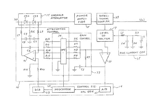
Referring now to Fig. 4, the description will
proceed to a level control device according to a preferred
embodiment of this invention. Similar parts are
designated by like reference numerals and symbols and are
operable with likewise named signals which have similarly
named levels or values indicated by like reference
symbols. It is presumed as described before that the
device input signal S(i) is an IF signal. The up
,,
2 0 9 7 7 2 9
converter 13 is not depicted merely for simplicity of
illustration.
The level detector 17 has a similar structure and
is not depicted in detail. The level detector 17 is,
however, accompanied by a bias current generator 31
connected to a point of connection between the first
capacitor Cl and the detector diode CDl which are
illustrated in Fig. 1. The level detector 17 is
controlled by a bias current supplied thereto from the
bias current generator 31.
The bias current generator 31 comprises a power
source 33 depicted as a battery. The power source 33 has
a source voltage which is typically 5 volts. Diodes,
resistors, and capacitors will be numbered hereinafter
serially continuing those used in the level detector 17.
A third resistor R3 and a first coil Ll are
connected in series between the power source 33 and the
point of connection of the first capacitor and the
detector diode. A fourth capacitor C4 and a fourth
resistor R4 are connected parallel between ground and a
point of connection between the third resistor and the
first coil.
The bias current develops a bias voltage at the
point of connection between the second resistor R2 (Fig.
1) and the point of connection of the first resistor Rl
and the third capacitor C3, both depicted in Fig. 1. The
bias current has a bias current value determined by
circuit constants of the level detector 17 and the bias
16 ~ O 9 7 7 2 9
current generator 31, the source voltage of the power
source 33 inclusive.
The bias voltage does not appreciably depend on
the controlled output level as depicted in Fig. 2 by a
dashed line labelled V(b) but varies with the temperature
in compliance with temperature dependencies of the circuit
constants like the detected voltage.
Turning temporarily to Fig. 5 with Fig. 4
continuously referred to, temperature is depicted along
the abscissa in ~C. Voltage is illustrated along the
ordinate in V. It will be assumed that the detected
voltage varies in the manner exemplified by a straight
line labelled V(d).
In accordance with this invention, the bias
current is selected so that the bias voltage may vary as
exemplified in Fig. 5 by another straight line labelled
V(b). More particularly, the circuit constants are
selected so that the bias voltage is given a substantially
constant difference from the detected voltage irrespective
of the temperature variation.
Turning back to Fig. 4, attention should be
directed to the fact that the level control device is used
in the TDM modulation system. Each of the device input
and output signals is therefore a succession of bursts.
The level detector 17 produces the detected signal with
the detected voltage related to the attenuated level,
namely, to the controlled output level, when the bursts
;~J
_ 17 ~0~772~
are on. The detected signal is given the bias voltage
alone when the bursts are off.
It will be surmised during a short while that the
detected signal is supplied directly to the control signal
generator 19. The input level varies between the detected
voltage and the bias voltage.
In the control signal generator 19, the AD
converter 23 converts the detected voltage and the bias
voltage to a first and a second digital value. The
processor 25 subtracts the second digital value from the
first digital value to derive a difference digital value,
which is substantially independent of the temperature
variation. Subsequently, the processor 25 compares the
difference digital value with the reference value to
derive a digital control value as the processed level
described before and to produce a processor output signal
having a digital processor output value proportional to
the digital control value. The DA converter 27 converts
the digital control value to an analog value to produce
the attenuation control signal with the analog value used
as the attenuation control level.
As a result, the attenuation control level is
substantially independent of the temperature variation.
Furthermore, the substantially temperature independent
digital value is useful in removing a slight error which
may be introduced into the controlled output level when
the bias voltage has not a completely constant difference
from the detected voltage. It is now possible to obviate
~ O ~ 7 7 2 9
18
the temperature error which would otherwise be introduced
into the controlled output level or power. This is
correct under the condition that the bias voltage is given
a substantially constant difference from the detected
voltage irrespective of the temperature variation.
However, even if the difference between the bias voltage
and the detected voltage varies in dependence on the
temperature variation, the present invention can reduce
the temperature error in the controlled output level in
comparison with the above-mentioned novel level control
device where only the detected voltage is compared with
the reference voltage to control the attenuator. This is
because, according to this invention, the difference
digital value is made which is a difference between the
bias voltage and the detected voltage, and is compared
with the reference digital value to produce the digital
control value. The processor output signal has the
digital processor output value proportional to the digital
control value. The processor output signal is DA
converted into the attenuation control signal which
controls the variable attenuator 11.
In Fig. 4, it is preferred that the detected
signal is not supplied directly to the control signal
generator 19 but through a single operational amplifier
which has a noninverted and an inverted input terminal and
an amplifier output terminal and serves as a variable gain
amplifier 35 having a variable gain. Supplied with the
detected signal as the noninverted input terminal,
2097729
lg
the variable gain amplifier 35 produces an amplifier
output signal fro~ the amplifier outpu~ ~e~minal for
supply to the ~ontr~l signal ~enerator 1~
Although dependent on the variable ~ain, the
amplifier output signal has an ampllfied voltage which i~
related to the de~e~ted voltage or ~he controlled output
level and is related to the bias vol~age Inasmuoh ~s
the ~ia~ ~ltage is ~iven the substantially conStant
differen~e from the deteoted voltage in the ampli~ier
ou~pu~ si~nal, the cont~ol ~ignal generator 1~ ls
operable in the ~anner described in the fore~oing. It
should, however, be noted that the control signal
generator 19 additionally produces the processor output
~ signal from ~he pro~essor 25.
A ga~n controller 37 comprise~ ~n ~n~log
multiplexer (MPX) 3g grounded and a fif~h resisto~ R5
connec~ed to ~he inver~ed i~put terminal and to ~he
a~plifier outpu~ ~erminal of the variable gain ~mpli~ier
35. The amplifie~ output terminal is grounded through a
fifth capacitor C~. In ~he example ~eing illustxa~ed,
sixth throu~h ninth resl~tors R6, R7, ~8, and ~, four in
number, are connected parallel bet~een the in~erted inpu~
terminal and the ~ul~iplexer 3g. Controlled by the
processor o~tpu~ si~nal, the multiplexe~ 39 grounds the
2~ inv~rted input termin~l through a sele~ted resistor of
the four re~is~ors R~ to R9 ~herethrough Inasmuch as
the sele~ted resi~tor is selected from the o~r regis~e~G
R6 to Rg, it is possible ~o use t~o binary bits as the
209772~
pro~ecsor output ~i~nal.
Controlled by the g~ln con~roller 37, the
variable gain ~mplifier ~5 ampli~ies the de~ec~ed signa~
~ith a ~re~ter gain ~hen the ~ontrolled ~u~pu~ level is
lower. Thi~ decreases the eonverter error small rela~ive
~o the v~lues processed in ~he con~rol sign~l ~enera~or
1~
In Fig. 4, ~he variable attenuator 11 comprises
~ir~t and ce~ond at~enuato~ diodes as se~ond and third
diodes CD2 ~nd C~3. The second and ~e third diodes are
typically PI~ diodes connected in ~eries to ha~e a point
of serie~ ~onne~tion therebetween. A combina~ion of ~he
~e~ond and the ~hird diodes ha~ ~n input end of the
~iab~e attenu~tor 11 supplied with the device inpu~
~iqnal and an o~t~L end of ~he varîable attenuator 11 a~
~hich the at~en~ator output signal is produ~ed~
Being used a~ ~he attenua~ion con~ol signal
supply a~range~ent 21, an attenuation ~ont~ol uni~ will
be designa~ed by the referen~e numeral 21 and sh~re~ t~e
~ultiplexer 3~ with t~e gain ~on~roller 37. In ~he
attenuation con~rol unit 21, a tenth ~esistor R10 is
supplied ~ith ~he at~enuation ~ontrol signal at its one
end. The other end is grounded thro~h an ele~en~h
resistor Rll.
A component opera~ional amplifier 41 ha~ a
noninverted and an lnverted input termin~l ~nd an
amplifier o~put terminal. A point of ~on~e~tion b~ween
the ~enth and the e~eventh resistors is ~onnected ~o the
2097729
21
nonin~e~ted inp~t ~e~minal. A pa~allel conne~tion of
t~elf~h through fifteenth resi~to~s R12, R13, R14, ~nd
~15, four in number, is connected between ~he inver~ed
input termin~l and the m~ltiplexe~ 3~. Con~rolled by ~e
processor o~put signal, the multi~lexer ~ grounds a
selected resisto~ of ~he four res~stors R12 through R15
the~eth~ough. The component operational amplifier 41 and
the selec~ed re~istor of t~e four re~istor~ ~re used ~s a
constan~ current circuit for compensatlng fo~ the
temperature error of the at~enuator diode~ CD2 and C~3.
In addi~ion, ea~h of ~he four resistors Rl2 through Rl~
i~prove~ the nonlinearity of ~he atten~ation
characteri~tic.
A sixth capacitor C~ ls ~onnected bet~een the
inverted inp~t terminal and ~he a~pli4ier outpu~ ~ermlnal
of ~he component operational amplifier 41. A se~ond coil
L2 is conne~ted ~o the inverted inpu~ ~erminal and to the
ou~p~t and of the v~riable attenuator 11 A seventh
capacitor C7 is connec~ed between ground and a point of
connection o~ the second coil to the inverted input
te~inal.
A third coil L3 i~ Gonnected to ~he amplifier
output terminal of the co~ponent operational ampl~fier 41
and to the input end of the variable attenuator 11 An
ei~hth capacitor ~8 is connected ~e~ween ground and a
point of connection of ~he third ~oil ~o the amplifier
output term~naL. A six~een~h resis~or R16 i~3 connected
~o the poin~ of series oonnection. A nin~h Gapaci~or C~
2097729
'
22
grounds ~he sixteenth resistor~
~ eview~n~ Fig. 4, it is now unde~stood tha~ *~e
variable g~in amplifier 35 and the gain ~ontrolle~ 37 are
cooper~ive ~o serve as an amplifyin~ arrangement fo~
S amplifying the detected ~gn~l ~ith a higher ~ain
c~rresponding to a lower level o~ the ~ontrolled ou~pu~
po~er or le~el The attenu~ion control unit 21 serve
~s an a~enua~ing a~ran~ement fo~ at~enuating the
a~tenua~ion control level with a greater a~ount of
attenu~ion ~hlch ~orre~ponds to the lo~er level of the
controlled outpu~ level, namely, to the higher gain~
Referring to Fig. 6 in addition to Fig. 4, it
will ~e ~u~mised ~ha~ ~he processor 25 ~on~rols operation
of the control signal gene~ator 19. Me~ely for b~e~i~
1~ of the description, it ~ill be a~.umed that ~he detected
signal is supplied direc~ly from ~he level detec~or 17 ~o
the con~ol signal generator 19.
At a first step 51, the pro~e~so~ 25 knows tha~
the bursts are off. At ~ ~econd s~ep ~2, ~he AD
2Q conver~r ~ conver~ ~he bias volta~e ~o the second
digi~al value At a thi~d step 5~, the pro~essor ~5
kno~s ~hat t~e ~rs~s are on. A~ a four~h s~ep 54, the
AD converter 23 converts the detected voltage to ~he
firs~ di~it~l ~alue~
At a fifth step 55, the processor 25 su~tra~ts
the second digital ~lue fro~ the first digit~l ~alue to
de~ive ~he differenGe di~ital ~alue~ ~t a ~ix~h ~tep ~6,
the pro~essor 25 ~al~ulates ~on~rol values which may be
~ 2097729
23
u~ed to control the level ~ontrol device.
A~ a sevent~ step 57, the processor ~ ~heck~
whether or no~ ~he difference digi~al va~ue is coLrect.
qhis ~heck is for Ghecklng whether or not the controlled
output po~er or level is corre~. If ~he con~rolled
outpu~ level is ~orre~, the seven~h s~ep ~7 is returned
to the first step ~l.
If ~he ~ontrolled output le~el is in~orrect at
the seven~ s~ep 57, the pro~essor 25 ~he~ks at an eighth
step 58 ~he~he~ o~ no~ ~he ~on~rolled o~tp~t level lc
hig~. If t~e ~on~rolled ou~p~t level is high, the
proGes~o~ 25 increa~e~ at a ninth step ~9 the attenuation
control level to de~rease ~he eon~rolled ou~pu~ level.
I~ the controlled output level is low, ~he processor 2$
lS increases a~ a ~enth s~ep 60 ~e controlled output level.
The ninth step S9 o~ the tenth step 60 is returned to the
first step 51.
~ evie~ing Figs. 4 through 6, the le~el ~on~ol
device is ex~ellently operable. Me~ely by ~y of
~0 exa~ple, let it be ascumed tha~ ~he l~el oon~ro~ device
is used in a mo~ile communication ~ystem of a cellular
type. ~hen ~ down-going si~nal i5 re~eived with a
~j ni mum level ~hich is n~t higher th~n minus 4 dBm, ~
conventional level control devi~e ~ad a de~e~ion error
of plus or ~inu~ ~ dB. ~he conversion errors of plu~ o~
minus 5 dB and lOdR were introduced into ~he eontrolled
outpu~ power by an A~ ~onverter and a DA converter~
When use is ~ade of ~he level control device
2097729
'
24
,
being illu~ra~ed, ~he dete~ion error waS reduced
~etween plus and minus 0.4 dB. The conversion error~ o~
the A~ con~er~er 23 and the DA converter 27 were
~ecrea~ed between plus and minus 0.5 dB and 0.4 dB. E~en
in a ~orst ~ase, ~he ~ontrolled ou~put power or level had
an outpu~ error between o~ly plu~ and min~ 1.3 d~. Four
parallel resistors R6 to R~ or R12 to R15 are ~ally
~ufficient
While this inven~ion ~as ~us far been described
10. in specific conjun~tion ~ith a single embodimen~ thereof,
it ~ill now be readily possible for one skilled in the
a~t to put this in~entiOn into practiGe in various o~er
mannerS, For example, a ~ariable gain amplifler i~ ~n
e~ivalent of the ~a~ le a~tenuato~ 11. It i~ po~sible
15 to modify ~he level de~ec~or 1~.