Note: Descriptions are shown in the official language in which they were submitted.
2 0 9 8 0 7 2
X-RAY MICROSCOPE WITH A DIRECT
CONVERSION TYPE X-RAY PHOTOCATHODE
DESCRIPTION
BACKGROU~nD OF I~DE ~VENTION
~ of the Inuent~n
The present invention generally relates to X-ray image
intensiflers and, more particularly to an X-ray microscope
utilizing a dlrect conversion X-ray photocathode in con~unction
with an electron multiplier.
D~sc~ption of the P~ior Art
X-ray to visible converters are well known in the art but
generally use indirect conversion techniques, where an X-ray
image is converted to visible light in a scintillator, the visible
light (photons) are then converted to a corresponding electron
15 image, and the electrons are multiplied and strike a phosphor
display screen to provide an enhanced directly viewable visible
image. There are numerous disadvantages in having to convert
an X-ray image to a visible light image before generating and
multiplying a corresponding electron image. Conversion o~ an
20 X-ray image to a visible light image is normally accomplished
by using a scintillator, as described in U.S. Patents No.
4.104,516, No.4,040,900, No.4,2S5,666, and No.4,300,046.
In each instance, the scintillator exhibits a limited response
time, poor spacial resolution and sensitivity, and due to the
.. ... - ................ . .
,' '' ~ ..
-- 2098072 !
complicated fabrication techniques and the attendant
requirement to use light shielding, the cost ls prohibitive.
In panel type X-ray image intensifiers, scintillation nolse
also becomes a problem, which mostly comes from the
5 exponential pulse height distribution of the micro channel plate
(MCP) gain.
SUll~ARY OF THE INVENTION
It is therefore an object of the present invenffon to
provide a photo-eIectron cathode, having specially designed
10 secondary electron emission layers, which will directly convert
an X-ray image to an equivalent electron image, while
exhibiting high efficiency, low noise, high speed and a broad
band x-ray photon detecffon capability.
The shortcomings of the prior art have been effectively
15 overcome by designing a direct conversion X-ray photo-electron
cathode consisting of a heavy metal layer which functions as an
X-ray absorber, and a transmission secondary electron
emission layer which funcffons as an electron mulffplier with a
mulffplication factor of twenty or more. It has been found that
20 by increasing the number of input electrons per channel of the
MCP by a factor of twenty or more, the scintillaffon noise is
drasffcally reduced. In the instant case, this is accomplished
by using a compound mulffplier, which is a direct conversion
type X-ray photocathode consisting of two parts. The flrst
25 being a heavy metal layer, which acts as an X-ray absorber,
and the second part being a transmission secondary electron
emission layer. The high energy photoelectrons produced in
CSL-002
- , , .
2098072'
the heavy metal layer are multiplied by the secondary electron
emitter to a factor of twenty or more. Due to this deslgn, the
noise of the intensifler is reduced and the sensitivity of the X-
ray photocathode is increased, especially in the high energy, X-
ray region.
A new panel type X-ray intensifier may be made by
integrating this new direct conversion X-ray cathode, a micro
channel plate and an output display fluorescent screen.
A portable projection type X-ray microscope may be made
by using the above X-ray intensifier, a micro-focus X-ray source
and a personal computer (PC) based image processing system.
The energy of the X-ray can be ad~usted and the magnification
can be changed by ad~usting the distance between the X-ray
source and the object. The low noise and high sensitivity of the
intensifier make it possible to achieve a large magnification. A
sub-micron X-ray microscope has also been designed for sub-
micron X-ray diagnostic purposes.
According to the invention, there is provided a photo-
electron cathode, for use in an X-ray microscope, capable of
directly converting an X-ray image to an equivalent electron
image which shows a substantially improved sensitivity and a
very low scintillation noise in the high energy X-ray region of
the frequency spectrum.
BRIEF DESCRIPTION OF THE DRAWINGS
The foregoing and other ob~ects, aspects and advantages
will be better understood from the following detailed description
of a preferred embodiment of the invention with reference to the
drawings, in which:
CSL-002
.
:.............. .
;
-" 2098072 ~
Figure 1 shows the dlrect conversion compound X-ray
photo-electron cathode of this invention;
Figure 2 shows a schematic diagram of a panel ~pe X-
ray image intensifier; and
Figure 3 depicts a portable projection type real time X-ray
microscope incorporating the X-ray photocathode of Figure 1.
CSL-002
. '
' -
-" ~ 2098072,
DETAILED DESCRIPrION OF A PREFERRED
EMBOD~OENT OF THE INVENTION
Referfing now to the drawings, and more particularly
to Figure 1, there is shown a diagram of the X-ray
5 photocathode. Element 6 is a substrate of light metal, such as
aluminum. The thickness is selected to assure its withstanding
the attracffon force from the high staffc electric fleld and does
not attenuate the X-ray intensity significantly. For 35-80 KV
X-ray, a 50 llm aluminum foil is suitable. Element 7 is the
10 heavy metal layer of the X-ray photocathode, which is a layer of
tantalum, tungsten, lead, bismuth, or gold. The optimum
thickness depends on the energy of the X-ray photon, the L or
K series criffcal excitaffon voltage and the density of the heavy
metal. Table 1 gives the opffmum thickness of different heavy
15 metals for 35-80 KV X-ray.
TABLE 1. O~rlMUM THICKNESS OF DIFFERENT HEAVY METALS.
¦ EnergyofX- _ _ e ==
I Ray 35 40 45 50 60 65 70 80
20 Optimum
Thickness (llm) _
W 0.5 0.7 59 1.2 191231 1
Ta 0.4 S _ 1.5 2.2 2 7 __
Au 0.4 0.6 0.8 1.1 1.7 _ 2.5 4
Pb 0.6 1.0 1.5 2.0 3.2 4.7 6.
I ___
¦ Bi 0 6 O 9 1 4 1 9 3 1 _ 4 6 2
CSL-OQ2
: ,- ', ' '
209807'2
Element 8 is the transmission secondary electron
emission layer of the X-ray photocathode, which comprises one
of the following materials whlch have a high secondary electron
emission coefficient: Csl, CsBr, KCl, CsCl or MgO. The cesium
5 iodide or cesium bromide layer can be coated in high vacuum
for a high density profile, or in certain pressure of inert gas,
such as argon, for a low density proflle. The optimum
- thickness of the cesium iodide or cesium bromide layer depends
on the energy of the photoelectron produced in the heavy metal
10 layer which is determined by the selection of the X-ray energy
and the specific heavy metal. For 60 KV X-ray and gold layer,
the optimum thickness of the ceslum iodide layer is
appro~dmately 7.4 ~lm for high density profile and 370 ,um for
low density profile, respectively. For the other heavy metals,
15 the optimum thickness of the normal and low density alkali
halides, respectively, in llms would be as follows: Bi - 6.8/340,
Ta - 8.2/410, Pb - 7.0/350, and W - 8.1/405. The secondary
electron conduction (SEC) gain of a low density profile cesium
iodide layer can be as high as 100. The low density profile of a
20 cesium iodide or cesium bromide layer can be prepared by
evaporating the bulk material in argon with pressure of about 2
torr, the resulting relative density of the layer is about 2%. A
cesium iodide secondary electron emission layer is also coated
on the input channel wall of the MCP. This emission layer has
25 a high density sub-layer and a low density sub-layer. The hlgh
density sub-layer is 1-2 llm with density of approximately 50%.
The low density sub-layer has a decreased density proflle from
the interface with the high density sub-layer to its emission
surface. The density distribution profile starts from 50% at the
30 interface and decreases to about 2% at the emisslon surface.
CSI~()02
,
- .. ,
'
-~ 2098072
The low density sub-layer is about 3-7 ~m.
Figure 2 is a schematic diagram of a panel type X-ray
image intensifier, with element 5 being an input window. The
window is made of 0.2 mm titanium foil. The thin Ti foil
reduces the scattering of the incident X-ray and has an
excellent transmission coefficient, especially for low energy X-
rays. Element 9 is an MCP and element 10 ls an output
display fluorescent screen coated on a glass window 11. In
operation, the voltage of the substrate 6 ranges between -1500V
and -2000V, with the voltage of the input surface of the MCP at
about -lOOOV and with the output surface of the MCP
grounded lV=O), the voltage of the output display fluorescent
screen should be around +8000V to ~lOOOOV. The brightness
of the image can be as high as 20 Cd/m2. The diameter of the
panel type X-ray image intensifier can be made from 50 mm to
200 mm with the thickness of the intensifier about 2 cm. This
panel type X-ray intensifler has a 1:1 input and output image
ratio and is vacuumed to 5 x 10⁻⁷ torr in a glass or ceramic
shell.
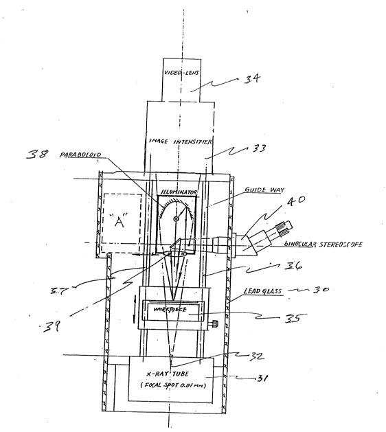
Figure 3 depicts a portable pro~ection type real time X-ray
microscope encased in a lead glass enclosure 30. An X-ray
source, shown as X-ray tube 31 is mounted in one end of the
enclosure and provides a 35 KV to 80 KV X-ray beam with a
spot size falling between a micron and a sub-micron, as shown
emanating from point 32. On the opposite end of the enclosure
30 is mounted an X-ray image intensifler 33, as described in
Figure 2, and is separated therefrom by about 300 mm to 1,000
mm, depending on the specific application. The video-camera
34 actually represents the means for viewing the X-ray image
presented at the output of the image intensifler and can be
CSL-002
2098072
either directly viewed or recorded by video. A vertically
adjustable workpiece 35 is mounted on a pair of transport rails
36 and 37 for adjusting the position of the item under study.
The geometrical ampl~fication Is therefore adlustable
5 continuously from 1 to 1,000 times. A parabolic illuminator
38 is for illumination of the object. lhe co-axial optical
microscope 40 and lens 39 are used for the alignment of the
object under test. The illuminrator 38 and lens 39 will be
moved to position "A" during the test.
While the invention has been described in terms of a
single preferred embodiment, those skilled in the art will
recognize that the invention can be practiced with modiflcation
within the spirit and scope of the appended claims.
CSL-002
,