Note: Descriptions are shown in the official language in which they were submitted.
~IC~0~08~W~ 2~ 2 ~ ~ 8 1 ~ O
High voltage trans~ormer for a television receiver
The invention i5 hased on a high voltage transtormer
according to the preamble o~ claim 1. Such a transformer is
known from DE-OS 35 14 308. Such transEormers genarate a
high voltage for television receivers in the order of
magnitude of 25 kV .
For television receivers with larger picture tubes
(kinescopest, for example, with an aspect ratio of 16:9 or a
screen diagonal ot 85 cm, greater high voltages in ~he order
o~ magnitude of 35 kV are required. qransformers for such
a great high voltage exhibit, unavoidably. an increased power
loss, thereby causing the build-up of heat to be greater and
increasing the geometrical dimensions reqlJired tor the
dissipation of the heat.
It is the object of the invention ~o reduce the power
dissipation at the transformer with such high voltage
transformers. This ~ask is solved by the invention
specified in clai~ 1. Further advantageous developments of
the invention are given in the subclaims.
The invention is firstly based upon an analysis of all
the types of losses which appear altogether with such a
transformer. A first type of 108R consists of ferrite
losses through magnetic reversal of the core corresponding
to the area formed by the hysteresis curve. Such losses can
only be reduced by the use of better quality ferrite
materials. A second type of 1088 consists of copper losses
through the oh~ic resistance oE the wire and the s~in
(Kelvin) effect. A third type of 1088 consists of losses in
the high voltage rectifier diodes, i.e~ through the rorward
(flow) voltage ànd the on-state current, the off-state
voltage and the off-state current, and ~he swirch:in(~ lossex
- ' '
~190/08/A~WP 2~11'31 - 2 - ~ 9 ~ -
upon switching over ~rom the blocked to ~he conduct;ing
states and vice versa. A four~h type o~ loss consists of
dielectric losses thro11gh displace1nent c1lrrents in ~he
insula~or ger1erally made from a sealing resin. As far as
the first three types of los~ are concerned, there are lower
limits caused by, in particular, techno~Logical reason6 and
the available componen~s. The invention now concentrates on
the fourth type of loss. In doing this the invention is
based on the following consideration. The dielectric losses
appear especially in the region between the primary winding
and the secondary or high voltage winding because it iB here
that the greatest voltages differences exist. Therefore, if
it were possible to successfully construct this region as
free from electrical fields as possible, then the dielectric
losses could be considerably reduced. With the invention
this is achieved merely by a particularly advantageous
division of the impulse voltages at the pri~ary winding and
the secondary winding in such a way that in this named
region the impulses have roughly the same amplitude and
polarity at the primary winding and at the secondar~
winding. 1'he difLerence between the impulse volta~3e:; in ~he
two windings is then practically lost so that, :in a desired
an1ler, a space is obtained which is f:ree fro1a electric
fields and losses through dielectric ctisplacement currents
are avoided a~ far as possible. A signl~icant advar1tage is
that the field-free space is achieved not ~hrough the use o~
additional means but rather only through a skil~ul
arrangement of the parts that are required anyway.
Furthermore, by reducing the dielectric displacement
currents in the insulator surrounding the windings, the
harmonic content of the voltages generated is reduced. This
leads to less natural re30nances which otherwise are caused
by displacmen~ currents. The reduction in the harmonic
waves causes an i~provement to the internal resistance and,
in addition, a~reduction of the acoust:ic noise appearing at
the transformer. Further, the material surrounding the
ll~)0/08/A~WP 28l191 - 3 - 20~
windings, preferably a cac;t resin, is also placed urlder less
s t: res~ .
The invention is explained in the following by means of
the drawing. Therein i8 showrl:
ig. 1 the configuration of a high volta~e ~rans~ormer
according to the invention, ancl
~ig. 2 a replacement circuit diagram for the tran~former
according to Fig. 1.
In the Eollowing description only the impulses voltages
effective at the transformer are talterl into consideration.
The direct voltages which appear are not considered b~allse
these cause no dielectric displacement currents and,
consequently, no power losses.
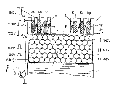
In Fig. 1 the coil former 7, carrying the primary
winding 3, is supported on the core 1. The primary winding
3 consists of six layers. The lead-out wire from the lower
layer is connectsd to the terminal 'b' wil:h the operatirlg
voltage +UB. The lead-ou~ wire from the upper layer is `:
connected to the terminal 'd' and to the switching
transistor 13 which is controlled by a line-frequency
switchi.ng voltage Z at terminal 'c'. The impulse vol~age at
~erminal 'b' is zero. The impulse voltage at termirlal 'd'
has the full value of ~he flyback voltage, i.e. ~1~00 V.
Therefore, the impulse voltage continually increases, from
winding to winding, from the value zero at terminal 'b' up
to the maximum value at terminal 'd'. q'his means that the
impulse voltage decreases by about l~ per cent over ~he
axial length of the upper layer of the winding ~ and tt~e
impulse voltage at the right-hand end of the upper layer has
a value of ~1000 V. The impulse voltage is, therefore,
essentially constant over the axial leng~h of the coil
i
~l~0/~8/A~WP 2~119L - ~ - 2 ~ 9 81 ~ O
forlller 7 in the upper layer o~ wind:ing ~ and ha-s a mean
~alue of 1100 V.
Arranged above the coil former 7 with the primary
windinc~t 3 is the compartment coil former 2 whic}l has a total
o~ 16 cells Ka through Kp ~separated by walls 8 which are
filled with partial windings 4a through 4p of the secondary
or high voltage winding 4. The lead-out wire ~rom the upper
layer of the first partial winding 9a i~ conrlected to
ground. Each of the lead-out wires at the base o~ a cell
i3 coupled to the anode of a high voltage rectifier diode 6
the cathodes of which are alway4 coupled to the lead-ou~
wire from the upper end of the following partial winding 9.
~rhe lead-out wire ~rom the bas~ o~ the linal partial winding ~`~
4p in cell ~p forms the high voltage terminal a . I`he
winding process for the entire secondary win~ing ~ scarts at
the base of cell Kp. As always one diode 6 is positioned
between each pair of cells 15 diodes 6 are provided ~or a ~ -
total of 16 cells K. A high voltage UH of 32 kV ensues at
terminal a . These values assumecl an impulse of +ll0~ V
results always at the base of each cell ~ which i'3 iderltiCal ~`
for all cells. An impulse of -130~ V re-;ults at the upper
end of winding 9.
Consequently impulses with an esselltially constant
amplitude of +1100 V are present along the upper layer of
winding 3. On the other hand as described above impulses
with the constan~ amplitude of ~1~00 V also ensue throug}l
the high voltage ~inding 9 in the region associated wilh the
winding 3 i.e. in the region of the lower ends of the
cells. Apart from that the impulse~ ~-tt windincg 3 and at;
winding 4 are isochronous. Therefore a voltage differerlce
practically no longer e4Yists be~ween the impulse.~3 a~ win(iing
3 and the impulses at winding 4 so that a space free from
electric fields results as indicated by the dotted line ~.
~90/08/A~P 2811~ 5 - 2 ~ 3 ~
The .impulses a~ the upper enli of the wind-i.ngs 9 i.n ~act
have the wrong neyat:ive polarity ~or ~uild.irlg the fi.eld-f.ree
space. However, ~he impul3e~ present at this point are
sufficiently d:is~ant from the primary windirl~ 3 tha~ t~ley no
longer cause any signi~icant displacement currerlts through
the insulator.
The upper end of the first winding 4a is connected to
ground and therefore conducts no impu1.se vol.~age while, on
the other hand, the lower end of the final winding 9p, which
is connected to ground via the capacitance of ~he picture
tube, also conducts no impulse voltage. The voltage ratios
of these two windings are, therefore, different with respect
to those of the other windinys 4b through 9o. fn order to
also produce the desired amplitude ratios betweer~ ~he
impulse voltages in this ragion, it is advantageous to, in
contrast to the remaining cells, only half spool the cells
Ka and Kp. The primary winding 3 is preferably wound ~rom
stranded conductor in order to keep the losses due to the
skin effect low.
Fig. 2 shows the replacemerlt ci.rcuit dia~ram associated
with Fig. 1. The capacitor 1.9, essen~i.ally formed by tt~e
anode terminal tanode layer) of picture tube L5, :
connected to the t:erminal 'a' conclllctirlg ~lle Illgtl
voltage UH. The diode 6b therelore corresponds to the f:irst
diode in Fig. 1 between the base o~ cell Ka and the lead-out
wire at the upper end of cell Kb. The :inal diode 6p
corresponds to the diode between the lower und of the
winding of cell Ko and the upper lead-out wire of the final
cell Kp.
It is also possible to sub-divide the primary winding 3
into several partial windings which lie adiacen~ each o~her
in the axial direction on the core 1 and are wired in
parallel be~ween the terminals 'b' and 'd'. C;erlerall.y, the
- : ~
,
H90/~8/A~WP 281:L~Y:I - 6 - 2 0 ~ g ~ O
amplitude at the upper layer of primary winding 3 varies
over the axial length. This can be taken into account in
that the cells Ka through Kp are filled accordingly
differently so that the impul~es of each o~ the partial
winding~ 4a through 9p also have correspondirlg:Ly differing
amplitudes at the bases of the cells. The filling Lactor
for the cells K with the partial windings ~ wou~.d then
decrease from the le~t- to the right-hand end of the coil
formers 7, 2, in the same way as the amplitude of the
impulses at the upper layer o~ win~lir~g ~ (iecrea~e~, ~rom, in
Fig. l, +1200 V to ~1000 V.
. ' .
`: ' ' . ' '
.. . .