Sélection de la langue

Search

Sommaire du brevet 2098100 

Énoncé de désistement de responsabilité concernant l'information provenant de tiers

Une partie des informations de ce site Web a été fournie par des sources externes. Le gouvernement du Canada n'assume aucune responsabilité concernant la précision, l'actualité ou la fiabilité des informations fournies par les sources externes. Les utilisateurs qui désirent employer cette information devraient consulter directement la source des informations. Le contenu fourni par les sources externes n'est pas assujetti aux exigences sur les langues officielles, la protection des renseignements personnels et l'accessibilité.

Disponibilité de l'Abrégé et des Revendications

L'apparition de différences dans le texte et l'image des Revendications et de l'Abrégé dépend du moment auquel le document est publié. Les textes des Revendications et de l'Abrégé sont affichés :

  • lorsque la demande peut être examinée par le public;
  • lorsque le brevet est émis (délivrance).
(12) Demande de brevet: (11) CA 2098100
(54) Titre français: TRANSFORMATEUR HAUTE TENSION
(54) Titre anglais: HIGH-VOLTAGE TRANSFORMER
Statut: Réputée abandonnée et au-delà du délai pour le rétablissement - en attente de la réponse à l’avis de communication rejetée
Données bibliographiques
(51) Classification internationale des brevets (CIB):
  • H01F 38/42 (2006.01)
(72) Inventeurs :
  • GOSEBERG, WALTER (Allemagne)
  • REICHOW, WOLFGANG (Allemagne)
  • SANDER, HANS-WERNER (Allemagne)
(73) Titulaires :
  • DEUTSCHE THOMSON-BRAMDT GMBH
(71) Demandeurs :
  • DEUTSCHE THOMSON-BRAMDT GMBH (Allemagne)
(74) Agent: SMART & BIGGAR LP
(74) Co-agent:
(45) Délivré:
(86) Date de dépôt PCT: 1991-12-03
(87) Mise à la disponibilité du public: 1992-06-11
Licence disponible: S.O.
Cédé au domaine public: S.O.
(25) Langue des documents déposés: Anglais

Traité de coopération en matière de brevets (PCT): Oui
(86) Numéro de la demande PCT: PCT/EP1991/002285
(87) Numéro de publication internationale PCT: EP1991002285
(85) Entrée nationale: 1993-06-09

(30) Données de priorité de la demande:
Numéro de la demande Pays / territoire Date
P 40 39 373.9 (Allemagne) 1990-12-10

Abrégés

Abrégé anglais


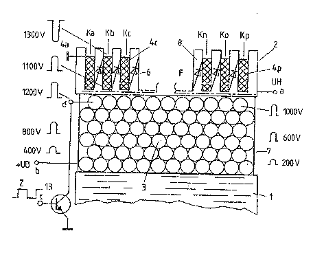
H90/08/A?WP 281191 - 10 -
ABSTRACT
1. High voltage transformer
2.1. With a high voltage transformer, in particular a
diode-split transformer, there generally exists the
requirement that the entire arrangement is, for reasons
of cost and weight, to be proportioned as small as
possible and likewise, the heat losses during operation
of such a high voltage transformer must be sufficiently
reduced so that the warming-up of the transformer does
not reach temperatures at which other circuit
components of a television receiver are damaged or
interfered with in a disturbing way. It is the task of
the invention to minimize the losses from a high
voltage transformer, in particular however, the
electrical losses.
2.2. According to the invention, for a high voltage
transformer of the aforementioned type the task is
solved in that a space is formed between the primary
winding and the high voltage winding which is almost
free of fields.
2.3. Television receivers, in particular television
receivers with a large number of lines for the HDTV
standard.
3. Fig. 1

Revendications

Note : Les revendications sont présentées dans la langue officielle dans laquelle elles ont été soumises.


H90/08/A*WP 281191 - 7 -
P a t e n t C l a i m s
1. High voltage transformer for a television receiver
with a primary winding (3) and a secondary winding (4)
arranged above this, the partial windings (4a through
4p) of which are located in cells (K) of a compartment
coil former (2) and are connected to each other via
diodes (6), c h a r a c t e r i z e d i n t h a t
the primary winding (3) and the secondary winding (9)
are sub-divided and polarized in such a way that they
produce impulses of roughly equal amplitude and
polarity in the regions of the windings (3, 4) adjacent
each other, and that a space almost free of electric
fields is formed between the windings (3, 4).
2. Transformer according to claim 1, c h a r -
a c t e r i z e d i n t h a t the primary winding
(3) is wound in layers with several layers lying above
each other and the lead-out wire (b) from the lower
layer is provided for connecting to the operating
voltage (UB) and the lead-out wire (d) from the upper
layer for connecting to a periodic switch (13).
3. Transformer according to claim 2, c h a r -
a c t e r i z e d i n t h a t the partial
windings (4a through 4p) are so polarized that there is
a positive-directed impulse always at the lead-out wire
from the base of each of the cells (K).
4. Transformer according to claim 3, c h a r -
a c t e r i z e d i n t h a t the number of cells
(K) and partial windings (4a through 4p) is
proportioned sufficiently large so that the positive-
directed impulse at the base of a cell (K) has
approximately the same amplitude as the positive-

H90/08/A*WP 281191 - 8 -
directed impulse at the upper layer of the primary
winding (3).
5. Transformer according to claim 1, c h a r -
a c t e r i z e d i n t h a t always one diode
(6) is connected via its anode to the lead-out wire
from the base of a cell (K) and the cathode of each
said diode is connected to the lead-out wire from the
upper layer of the partial winding (4) of the next cell
(K).
6. Transformer according to claim 1, c h a r -
a c t e r i z e d i n t h a t the start of the
winding for the secondary winding (4) forms the
terminal (a) supplying the high voltage (UH).
7. Transformer according to claim 1, c h a r -
a c t e r i z e d i n t h a t the primary winding
(3) consists of several partial windings (3a through
3c) wired in parallel which are arranged adjacent each
other in the axial direction of the coil former (2).
8. Transformer according to claim 1, c h a r -
a c t e r i z e d i n t h a t the transformer is
constructed as a diode-split transformer.
9. Transformer according to claim 1, c h a r -
a c t e r i z e d i n t h a t the cells (K) are
filled differently by the partial windings in such a
way that the impulses at the base of each cell have
roughly the same amplitude as the impulses at the
neighboring winding of the primary winding (3).
10. Transformer according to claim 1, c h a r -
a c t e r i z e d i n t h a t the first (Ka) and
the last (Kp) cells are, relative to the other

H90/08/A*WP 2831191 - 9 -
cells (Kb through Ko), only half filled with the
partial windings (4).

Description

Note : Les descriptions sont présentées dans la langue officielle dans laquelle elles ont été soumises.


~IC~0~08~W~ 2~ 2 ~ ~ 8 1 ~ O
High voltage trans~ormer for a television receiver
The invention i5 hased on a high voltage transtormer
according to the preamble o~ claim 1. Such a transformer is
known from DE-OS 35 14 308. Such transEormers genarate a
high voltage for television receivers in the order of
magnitude of 25 kV .
For television receivers with larger picture tubes
(kinescopest, for example, with an aspect ratio of 16:9 or a
screen diagonal ot 85 cm, greater high voltages in ~he order
o~ magnitude of 35 kV are required. qransformers for such
a great high voltage exhibit, unavoidably. an increased power
loss, thereby causing the build-up of heat to be greater and
increasing the geometrical dimensions reqlJired tor the
dissipation of the heat.
It is the object of the invention ~o reduce the power
dissipation at the transformer with such high voltage
transformers. This ~ask is solved by the invention
specified in clai~ 1. Further advantageous developments of
the invention are given in the subclaims.
The invention is firstly based upon an analysis of all
the types of losses which appear altogether with such a
transformer. A first type of 108R consists of ferrite
losses through magnetic reversal of the core corresponding
to the area formed by the hysteresis curve. Such losses can
only be reduced by the use of better quality ferrite
materials. A second type of 1088 consists of copper losses
through the oh~ic resistance oE the wire and the s~in
(Kelvin) effect. A third type of 1088 consists of losses in
the high voltage rectifier diodes, i.e~ through the rorward
(flow) voltage ànd the on-state current, the off-state
voltage and the off-state current, and ~he swirch:in(~ lossex
- ' '

~190/08/A~WP 2~11'31 - 2 - ~ 9 ~ -
upon switching over ~rom the blocked to ~he conduct;ing
states and vice versa. A four~h type o~ loss consists of
dielectric losses thro11gh displace1nent c1lrrents in ~he
insula~or ger1erally made from a sealing resin. As far as
the first three types of los~ are concerned, there are lower
limits caused by, in particular, techno~Logical reason6 and
the available componen~s. The invention now concentrates on
the fourth type of loss. In doing this the invention is
based on the following consideration. The dielectric losses
appear especially in the region between the primary winding
and the secondary or high voltage winding because it iB here
that the greatest voltages differences exist. Therefore, if
it were possible to successfully construct this region as
free from electrical fields as possible, then the dielectric
losses could be considerably reduced. With the invention
this is achieved merely by a particularly advantageous
division of the impulse voltages at the pri~ary winding and
the secondary winding in such a way that in this named
region the impulses have roughly the same amplitude and
polarity at the primary winding and at the secondar~
winding. 1'he difLerence between the impulse volta~3e:; in ~he
two windings is then practically lost so that, :in a desired
an1ler, a space is obtained which is f:ree fro1a electric
fields and losses through dielectric ctisplacement currents
are avoided a~ far as possible. A signl~icant advar1tage is
that the field-free space is achieved not ~hrough the use o~
additional means but rather only through a skil~ul
arrangement of the parts that are required anyway.
Furthermore, by reducing the dielectric displacement
currents in the insulator surrounding the windings, the
harmonic content of the voltages generated is reduced. This
leads to less natural re30nances which otherwise are caused
by displacmen~ currents. The reduction in the harmonic
waves causes an i~provement to the internal resistance and,
in addition, a~reduction of the acoust:ic noise appearing at
the transformer. Further, the material surrounding the

ll~)0/08/A~WP 28l191 - 3 - 20~
windings, preferably a cac;t resin, is also placed urlder less
s t: res~ .
The invention is explained in the following by means of
the drawing. Therein i8 showrl:
ig. 1 the configuration of a high volta~e ~rans~ormer
according to the invention, ancl
~ig. 2 a replacement circuit diagram for the tran~former
according to Fig. 1.
In the Eollowing description only the impulses voltages
effective at the transformer are talterl into consideration.
The direct voltages which appear are not considered b~allse
these cause no dielectric displacement currents and,
consequently, no power losses.
In Fig. 1 the coil former 7, carrying the primary
winding 3, is supported on the core 1. The primary winding
3 consists of six layers. The lead-out wire from the lower
layer is connectsd to the terminal 'b' wil:h the operatirlg
voltage +UB. The lead-ou~ wire from the upper layer is `:
connected to the terminal 'd' and to the switching
transistor 13 which is controlled by a line-frequency
switchi.ng voltage Z at terminal 'c'. The impulse vol~age at
~erminal 'b' is zero. The impulse voltage at termirlal 'd'
has the full value of ~he flyback voltage, i.e. ~1~00 V.
Therefore, the impulse voltage continually increases, from
winding to winding, from the value zero at terminal 'b' up
to the maximum value at terminal 'd'. q'his means that the
impulse voltage decreases by about l~ per cent over ~he
axial length of the upper layer of the winding ~ and tt~e
impulse voltage at the right-hand end of the upper layer has
a value of ~1000 V. The impulse voltage is, therefore,
essentially constant over the axial leng~h of the coil
i

~l~0/~8/A~WP 2~119L - ~ - 2 ~ 9 81 ~ O
forlller 7 in the upper layer o~ wind:ing ~ and ha-s a mean
~alue of 1100 V.
Arranged above the coil former 7 with the primary
windinc~t 3 is the compartment coil former 2 whic}l has a total
o~ 16 cells Ka through Kp ~separated by walls 8 which are
filled with partial windings 4a through 4p of the secondary
or high voltage winding 4. The lead-out wire ~rom the upper
layer of the first partial winding 9a i~ conrlected to
ground. Each of the lead-out wires at the base o~ a cell
i3 coupled to the anode of a high voltage rectifier diode 6
the cathodes of which are alway4 coupled to the lead-ou~
wire from the upper end of the following partial winding 9.
~rhe lead-out wire ~rom the bas~ o~ the linal partial winding ~`~
4p in cell ~p forms the high voltage terminal a . I`he
winding process for the entire secondary win~ing ~ scarts at
the base of cell Kp. As always one diode 6 is positioned
between each pair of cells 15 diodes 6 are provided ~or a ~ -
total of 16 cells K. A high voltage UH of 32 kV ensues at
terminal a . These values assumecl an impulse of +ll0~ V
results always at the base of each cell ~ which i'3 iderltiCal ~`
for all cells. An impulse of -130~ V re-;ults at the upper
end of winding 9.
Consequently impulses with an esselltially constant
amplitude of +1100 V are present along the upper layer of
winding 3. On the other hand as described above impulses
with the constan~ amplitude of ~1~00 V also ensue throug}l
the high voltage ~inding 9 in the region associated wilh the
winding 3 i.e. in the region of the lower ends of the
cells. Apart from that the impulse~ ~-tt windincg 3 and at;
winding 4 are isochronous. Therefore a voltage differerlce
practically no longer e4Yists be~ween the impulse.~3 a~ win(iing
3 and the impulses at winding 4 so that a space free from
electric fields results as indicated by the dotted line ~.

~90/08/A~P 2811~ 5 - 2 ~ 3 ~
The .impulses a~ the upper enli of the wind-i.ngs 9 i.n ~act
have the wrong neyat:ive polarity ~or ~uild.irlg the fi.eld-f.ree
space. However, ~he impul3e~ present at this point are
sufficiently d:is~ant from the primary windirl~ 3 tha~ t~ley no
longer cause any signi~icant displacement currerlts through
the insulator.
The upper end of the first winding 4a is connected to
ground and therefore conducts no impu1.se vol.~age while, on
the other hand, the lower end of the final winding 9p, which
is connected to ground via the capacitance of ~he picture
tube, also conducts no impulse voltage. The voltage ratios
of these two windings are, therefore, different with respect
to those of the other windinys 4b through 9o. fn order to
also produce the desired amplitude ratios betweer~ ~he
impulse voltages in this ragion, it is advantageous to, in
contrast to the remaining cells, only half spool the cells
Ka and Kp. The primary winding 3 is preferably wound ~rom
stranded conductor in order to keep the losses due to the
skin effect low.
Fig. 2 shows the replacemerlt ci.rcuit dia~ram associated
with Fig. 1. The capacitor 1.9, essen~i.ally formed by tt~e
anode terminal tanode layer) of picture tube L5, :
connected to the t:erminal 'a' conclllctirlg ~lle Illgtl
voltage UH. The diode 6b therelore corresponds to the f:irst
diode in Fig. 1 between the base o~ cell Ka and the lead-out
wire at the upper end of cell Kb. The :inal diode 6p
corresponds to the diode between the lower und of the
winding of cell Ko and the upper lead-out wire of the final
cell Kp.
It is also possible to sub-divide the primary winding 3
into several partial windings which lie adiacen~ each o~her
in the axial direction on the core 1 and are wired in
parallel be~ween the terminals 'b' and 'd'. C;erlerall.y, the
- : ~
,

H90/~8/A~WP 281:L~Y:I - 6 - 2 0 ~ g ~ O
amplitude at the upper layer of primary winding 3 varies
over the axial length. This can be taken into account in
that the cells Ka through Kp are filled accordingly
differently so that the impul~es of each o~ the partial
winding~ 4a through 9p also have correspondirlg:Ly differing
amplitudes at the bases of the cells. The filling Lactor
for the cells K with the partial windings ~ wou~.d then
decrease from the le~t- to the right-hand end of the coil
formers 7, 2, in the same way as the amplitude of the
impulses at the upper layer o~ win~lir~g ~ (iecrea~e~, ~rom, in
Fig. l, +1200 V to ~1000 V.
. ' .
`: ' ' . ' '
.. . .

Dessin représentatif
Une figure unique qui représente un dessin illustrant l'invention.
États administratifs

2024-08-01 : Dans le cadre de la transition vers les Brevets de nouvelle génération (BNG), la base de données sur les brevets canadiens (BDBC) contient désormais un Historique d'événement plus détaillé, qui reproduit le Journal des événements de notre nouvelle solution interne.

Veuillez noter que les événements débutant par « Inactive : » se réfèrent à des événements qui ne sont plus utilisés dans notre nouvelle solution interne.

Pour une meilleure compréhension de l'état de la demande ou brevet qui figure sur cette page, la rubrique Mise en garde , et les descriptions de Brevet , Historique d'événement , Taxes périodiques et Historique des paiements devraient être consultées.

Historique d'événement

Description Date
Inactive : CIB désactivée 2011-07-27
Inactive : CIB dérivée en 1re pos. est < 2006-03-11
Inactive : CIB de MCD 2006-03-11
Demande non rétablie avant l'échéance 1999-12-03
Réputée abandonnée - omission de répondre à un avis sur les taxes pour le maintien en état 1999-12-03
Inactive : Morte - RE jamais faite 1999-12-03
Inactive : Abandon.-RE+surtaxe impayées-Corr envoyée 1998-12-03
Demande publiée (accessible au public) 1992-06-11

Historique d'abandonnement

Date d'abandonnement Raison Date de rétablissement
1999-12-03

Taxes périodiques

Le dernier paiement a été reçu le 1998-07-20

Avis : Si le paiement en totalité n'a pas été reçu au plus tard à la date indiquée, une taxe supplémentaire peut être imposée, soit une des taxes suivantes :

  • taxe de rétablissement ;
  • taxe pour paiement en souffrance ; ou
  • taxe additionnelle pour le renversement d'une péremption réputée.

Les taxes sur les brevets sont ajustées au 1er janvier de chaque année. Les montants ci-dessus sont les montants actuels s'ils sont reçus au plus tard le 31 décembre de l'année en cours.
Veuillez vous référer à la page web des taxes sur les brevets de l'OPIC pour voir tous les montants actuels des taxes.

Historique des taxes

Type de taxes Anniversaire Échéance Date payée
TM (demande, 6e anniv.) - générale 06 1997-12-03 1997-11-05
TM (demande, 7e anniv.) - générale 07 1998-12-03 1998-07-20
Titulaires au dossier

Les titulaires actuels et antérieures au dossier sont affichés en ordre alphabétique.

Titulaires actuels au dossier
DEUTSCHE THOMSON-BRAMDT GMBH
Titulaires antérieures au dossier
HANS-WERNER SANDER
WALTER GOSEBERG
WOLFGANG REICHOW
Les propriétaires antérieurs qui ne figurent pas dans la liste des « Propriétaires au dossier » apparaîtront dans d'autres documents au dossier.
Documents

Pour visionner les fichiers sélectionnés, entrer le code reCAPTCHA :


Pour visualiser une image, cliquer sur un lien dans la colonne description du document (Temporairement non-disponible). Pour télécharger l'image (les images), cliquer l'une ou plusieurs cases à cocher dans la première colonne et ensuite cliquer sur le bouton "Télécharger sélection en format PDF (archive Zip)" ou le bouton "Télécharger sélection (en un fichier PDF fusionné)".

Liste des documents de brevet publiés et non publiés sur la BDBC .

Si vous avez des difficultés à accéder au contenu, veuillez communiquer avec le Centre de services à la clientèle au 1-866-997-1936, ou envoyer un courriel au Centre de service à la clientèle de l'OPIC.

({010=Tous les documents, 020=Au moment du dépôt, 030=Au moment de la mise à la disponibilité du public, 040=À la délivrance, 050=Examen, 060=Correspondance reçue, 070=Divers, 080=Correspondance envoyée, 090=Paiement})


Description du
Document 
Date
(aaaa-mm-jj) 
Nombre de pages   Taille de l'image (Ko) 
Revendications 1992-06-10 3 77
Abrégé 1992-06-10 1 27
Dessins 1992-06-10 1 46
Description 1992-06-10 6 224
Dessin représentatif 1999-08-17 1 26
Rappel - requête d'examen 1998-08-04 1 129
Courtoisie - Lettre d'abandon (requête d'examen) 1999-01-13 1 171
Courtoisie - Lettre d'abandon (taxe de maintien en état) 2000-01-03 1 185
Taxes 1996-07-03 1 43
Taxes 1995-07-12 1 43
Taxes 1994-07-05 1 50
Taxes 1993-06-08 1 34
Rapport d'examen préliminaire international 1993-06-08 11 329