Note: Descriptions are shown in the official language in which they were submitted.
fV~ 92111595 ~, ~ ~ ~ r~ ~~, ~ PCf/SE91/00~50
z
A Method to Reduce the Power Consumation of a Digital Filter
Bank by Reducing the Number of Multiplications.
'fhe present invention relates to a digital filter bank
intended for use, for instance, in battery-operated
applications, in which power consumption is decreased by
reducing the number of multiplications performed in the
filter bank.
In digital signal processing, there is a need in many
different conteaets to minimize the power consumption in
a given system. This may apply, for instance, to
battery-operated applications. Digital filters are
often more power consuming that corresponding analog
filters. The reason why the power. consumption of digi-
tal filtering processes is relatively high, is because a
large number of operations are often carried out each
second. Band filtering with the aid of filter banks is
one filtering method that is often used. The filter
bank can be-used when a number of frequency bands are ~o
be separated, or when it is desired to amplify different
. frequency bands to different degrees of amplification.
i~7hen bandpass filtering with the aid of a digital filter
bank, a high degree number is often required on the
filters included in the bank, in order for the filter
bank to be sufficiently selected. Hligher degree numbers ~,
imply many multiplications per sample and per second.
In digital filtration processes, the power consumed is
often proportional to the number of coefficients (multi-
plications) in the filter impulse response. power
consumption can therefore be reduced by reducing the
number of multiplica~ions. This is achieved in accord-
ance with the invention with a digital filter bank which
includes;
~~~' ~'~°
V'O 9211 ifi9b ~ ~ ~ ~ ~'~ :~ ~ PCTi~E9ila0~6U
f'.. '';!
A .zero-filled digital basic filter having a complement-
ary output, wherein the zero-filled filter relates to a
filter, which may be based on an LP-filter, which can be
expanded with a number of zero-value filter coefficients '
between each coefficient in the original filter; and
downstream mutually parallel part-filter banks;
wherein the passband of the basic filter and the pass-
band of the complementary output of said basic filter
define the filter-bank band;
l0 wherein one of the part-filter banks connected to the
normal output of the basic filter is intended to filter-
out those filter-bank bands which are pass bands to the
basic filter, so that only one of the filter-bank bands
is present on each signal from said one part--filter
bank; and wherein the other part-filter bank connected
to the complementary output of the basic filter is
intended to filter-out those filter-bank bands which are
pass bands to the complementary output of the basic
filter, so that only one filter-bank band is found on
each output signal from said other part-filter bank.
The term filter-bank band as used here and in the fol-
lowing is intended to denote one of the frec~uenoy bands
present in the output signals of the filter bank.
Preferred embodiments .of the novel filter bank are set
forth in the dependent claims.
r
xhe invention will now be described in mare detail with
reference to the a~company~.ng drawings, in which
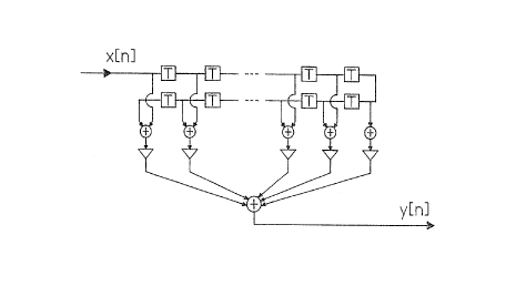
Figure 1 illustrates a linear phase FzR-filter of uni-
form degree number, where the number of multiplica~tions
has been reduced to almost half;
Figure 2 illustrates a linear phase FTR-filter with a
»
't3 92/1166 ~ ~ (~ ~ ~'y ~ .~. P~lfl5E91/a~7~~~
3
complementary output;
Figure 3 illustrates a zero-filled FTR-filter, iahich has
been constructed by replacing each time delay in the
filter illustrated in Figure 4 with four time delays;
Figure 4 illustrates a digital FIR--filter
Figure 5 illustrates the magnitude function of a linear-
1o phase lowpass FIR-filter of degree 6, which can be
realized with four multiplications per sample in accord-
ance with Figure 1;
Figure 6 illustrates the magnitude function of a zero-
filled digital filter which has been constructed by
replacing each time shift in the filter illustrated in
Figure 5 with four time shifts; this filter can also be
realized with four multiplications per sample;
2o Figure 7 illustrates a filter bank comprising a basic
filter and downstream part-filter banks:
Figure 8 illustrates a zexo-filled linear-phase FTR-
filter having a complementary output;
Figure 9 illustrates the ideal magnitude function of the
basic :filter with complementary output;
Figure 10 is an idealized diagram relating to the fre-
3o quency content of the outputs of two part-filter banks
TiD1 and ~xD2, said frequency content being the filter-
bank bandsa
Figure 11 illustrates embodiments of part-filter banks;
3~
Figure 12 illustrates an example of a filter bank having
'''~~i~ a~.~~
eve ~zm s9s ~~ rris~9~ ioo~~o
nine filter-bank bands; and
Figures 13a-13h illustrate the.magnitude function of
different filters H1(z), H2(z), H3(z), H~(z). H5(L),
H6(z), H~(z) and H8(z) in one eacample having a filter
bank with nine filter-bank bands.
one type of filter that has good properties is a linear
phase FIR-filter (Finite Impulse Response). The impulse
2o response of this filter is symmetrical and is described
by h~k) ° h(N-k), where k=0, ..., N-l, where N is the
degree number of the filter. When realizing such a
falter, it is therefore possible.to half directly the
number of multiplications with the aid of a suitable
25 structure; see Figure 1. The linear phase FIR-filter is
described in more detail in "Multirate Digital Signal
Processing" by R.E. Crochiere and Z.R. Rabiner,
Prentice-Hall, 2983. This publication also describes
the configuration of a linear phase FIR-filter with the
0 so-called Remez-algorithm. r
Two filters, H(z) and Hc(z) are complementary when they
fulfil the condition:
i H(z) + Hc(z) i = 1 for all ;z~ = 1
Thus, when the filters have the same input signal and
the output signals are added together, the rESUlt is the
same as when the input signal has been delayed in cor-
respondence with the group -transit time of the
3o filters.
The complementary output signal Hc(z) can be obtained '
from a linear phase FIR-filter H(z) having a uniform
degree number N, from the relationship:
35 gc(Z) = z-Hf2 _ H(z)
Wa 9m~~3s9~ ~ ~ ~ ~ ~ ~~". .~ PCf/SE91/00860
Figure 2 shows that the complementary output Hc(z) can
be obtained in a very si~aple manner, when the filter
H(z) is a linear phase FIR-filter of uniform degree
number, which is realized in the form of a transversal
5 filter.
Complementary FIR-filters are described in more detail
in "Handbook of Digital Signal Processing'~, published by
D.F. ~lliott, chapter 2, by P.P. Vaieyanathan, with the
title "Design Implementatian.of Digital FIR Filters",
Academic Press, 1987.
A zero-filled filter is a filter which has been expanded
with a number of zero-value filter coefficients between
each filter coefficient in the.original filter. This is
identical to obtaining the transfer function H (z) of
hero
the zero-filled filter by replacing z in the transfer
function H(z) of the original filter with zn+1, where n
is the number of zero-value filter coefficients between
each filter coefficient in the original filter. In
other words:
Hzero(z) - H(zn+1),
For example: H(z) = a0 D a1*z 1,
n = 2
Hzero(z) - H(z3) ~ a0 + a1*z-3 ~.
a0, + 0*z-~' + 0*z-2 -E- a1*z-3
It is possible to beg~.n with an LP-filter having a
relatively short impulse response, and then expand the ..
filter with a plurality of zero-value coefficients
between each coefficient in the original filter. This
is achieved by replacing each time shift in the original
fzlter with a plurality of time shifts. The zero-filled
wo ~~ms~s
PCC/~F91 /00~6U
. ,:, s
6
filter shown in. Figure 3 has been obtained by expanding
the filter shown in Figure 41 with three zeros between
each filter coefficient. This results in an increase in
the degree number, without increasing the number of '
multiplications. This can be interpreted spectrally as
though the frequency characteristic is compressed and '
repeated along the frequency axis. This occurs because
the frequency characteristic of a digital filter is
periodic with the sampling frequency f . The result is
s
to a filter haring more stop bands with pass hands. These
filters are steep in relation to the number of multipli-
cations used.
The frequency characteristic of a zero-filled filter is
characterized by:
' Hzero(z) i = i H(zl+n) i
where H is the original filter, H is the zero-filled
zero
filter and n is the number of zero-value filter coeffi-
cients between each coefficient in the original filter.
2o This can also be eXpressed in the frequency plane
(z = e~*2~p1*f~Tj
Hzero(f ) t - i ~( (n -~ 1)'~f ) ;
Figures 5 and 6 illustrate an example of a lowpass.
filter which has been expanded with three zeros between
each coefficient.
Filters which are antisymmetric around half the sampling
fbequency also have in the impulse response a number of
coefficients which are equal to zero.
The inventive, novel filter bank construction will be
seen from a structure according to Figure 7. The con-
struction is based on a basic filter H1(z) and down-
stream part-filter banks H~i and HD2. The basic falter
2W~'~~:~.
wt~ ~~i r 1 ~~s Pcc r>s~9a ioo~6o
Hl(z) is a zero-filled linear phase FIR--filter. with a
complementary output (Figuxe 8). This filter z~ able to
separate effectively mutually adjacent filter-bank bands
with high degree numbers but with few multiplications.
Figure 9 illustrates an idealized configuration of the
frequency characteristic of the basic filter H1(z} and
its complementary.
Figure 13a illustrates an example of the frequency
characteristic of a basic filter having three multipli-
cations in a filter bank with nine outputs (nine filter-
bank bands}. The complementary output of the basic
filter has pass bands when the basic filter has stop
bands, and vice versa~
The basic filter and its complementary (Figure 7) di-
vides the input signal x(n) into two parts such as to
separate al.l mutually adjacent ~i~.ter-bank bands, so
that .each alternate filter-bank band is transferred to
the output signal yl(n) and the remaining filter-bank
bands are transferred to the complementary output
ylc(n). By choosing a zero-filled filter as the basic y
filter, the majority of the filter coefficients will be w
,equal to zero. It is therefore possible to use basic
filters having very high degree numbers to achieve good
separation between different filter--bank bands with the ,.
aid of a few multiplications.
The remainder of the structure, the part--filter banks,
is used to separate the individual filter-bank bands, so
that only one filter-bank band will be found in each
output signal.
Figure 10 illustrates an idealized form of the frequency
characteristic of.the,filter bank from the input on the
wo 9?/11s9s
Pt.'T/SF911t10860 --,.
basic filter Hl(z) to the'outputs of the part-filter
banks HD1 and HD2. Thus, the number of falter-bank
bands (output signals from the filter bank) :i.s defined
by the basic filter and its complementary. '
Different embodiments of the part-filter banks are '
comprised of one or more introductory filters and op-
tionally downstream part-filter banks, in accordance
with Figure 11.
The number of multiplications is reduced because:
- The basic filter is zero-filled and therefore is able
to filter-out each alternate frequency band with only ~
few multiplications;
- The complementary of the basic filter is obtained
with solely one subtraction; and
- The stop bands in the basic filter can be used as
transition bands in the subsequent filters, thereby
enabling the demands placed on the subsequent falters to
be reduced.
It should be noted that the number of bands in the
filter bank is defined by the basic filter and its
complementary.
Figures 12 and 13 illustrate an example where nice '
filter-bank bands are desired. The basic filter is
constructed in accordance with Figure 13a, as a linear
phase eamplementary FIR-filter with five pass bands
(faun pass bands for the complementary). HD1 (HD2) is a
part-filter bank accarding, to Figure 11a, and is com-
prised of an introductory linear phase complementary
FIR-filter H2(z) (H3(z)), according to Figure 13b
(Figure,l3c), and two subsequent part-filter banks, HD3
arid HD~ (HD5 and HD6) (Figure 12). H2(z) (H3(z)) is
.vc~ 9~r~ a ~9~ ~ ~~ ~ ~ ~ ~, ~ ~t-rrs~~a roo~6o
9
constructed as a zero-filled linear phase complementary
FIR-filter, so that said filter obtains pass bands for
each alternate pass band from the basic filter (the
complementary of the basic filter), but having a lower
degree of zero-filling n than the basic filter (the
complementary of the basic filter).
The arrangement' or array, can be repeated so that only
one filter-bank band is found on each output from each
part-filter bank. Accordingly, HD3' HD4' HD5 and HD6
will consist of an introductory linear phase complemen-
tary FIR-filter H4(z), H5(z), H6(z) and H,~(z) respec-
tively, and possibly of subsequent part-filter banks.
The complementary of .the filter H4(z) and H5(z), H6(z)
and H~(z) and their complements contain only one filter-
bank band and consequently have no subsequent part-
filter banks. Only HD~ is a subsequent part-filter
bank, since the output signal from H4(z) contains more
than one ( two ) f i lter--bank bands .
The Configurations in this filter bank are as follows: ..
HD1 and H02 accarding to Figure lla, HD3 according to
Figure lle, and Hp4, HDS, HD6 and HD~ according to
Figure llc.
The filters whose magnitude functions are given in the
Figures 13a-13h have the following zero-separated.
filter coefficients:
Filter H1(z)%
h(0) ~ h(48)
H(16) = H(32}
H(24}
Remaining coefficients are equal to zero. This filter
can thus be realized with three ~aultiplications.
WO 92111696 .i - ~CI~/~~91/O~D860 ,
Filter H2(z);
h(0) ~ h(24)
h(g) = h(16) ,
h(12) '
5
Remaining coefficients are equal to zero. This filter '
can thus be realized with three-multipliaations.
Filter H3(z);
to h(o) = h(3o) w
h(2) - h(~8)
h(~) _ h(26)
h(6) = h(24)
h(g) = h(~2)
h(10) = h(20)
h(12) = h(18)
h(a.~) = h(ls)
h(15) _
;W4~ 92/l ~ b9b ~ ~ ~ J r~ ~ ~. PC'I'/SE91 /~0~6~3
11
Remaining coefficients are eaual to zero. This filter
is a l0-degree falter, but can be realized with four
multiplications. .
Filter H~(z);
- h(8)
h(1) = h(~)
h(2) ~ h(6) .:
h(3) = h(5)
h(4)
This filter is an 8--degree filter, but can be realized
with five muitiplications. ..
ee~~o ~zn ~ ~~s ? ~ c~ ~ ; ..~ ~ ~~~i~~9~ ioo~~o ,.,-:-.
~. z
Then Hpl and H~2 are constructed in accordance with the
embodiment shown in Figure ,llb, a filter filters out
each filter-bank band from the basic ,filter. The advan-
tage with -this embodiment, as compared with a filter
bank constructed with parallel bandpass filters directly
from the input signal, is that the demands on the fil- '
ters downstream of the basic filter can be reduced. The
transition band between pass band and stop band can be
broadened, since each alternate filter-bank band can be
filtered out. This enables the number of multiplica-
tions to be reduced.